


Texas Instruments TL594CDR, TL594CD, TL594IN, TL594IDR, TL594ID Datasheet
...TL594
PULSE-WIDTH-MODULATION CONTROL CIRCUITS
SLVS052C ± APRIL 1988 ± REVISED JULY 1999
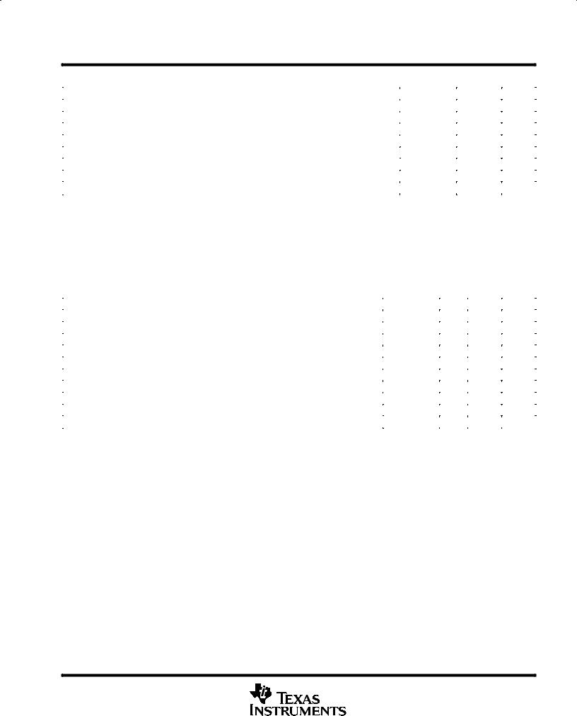
D Complete PWM Power Control Circuitry |
D OR N PACKAGE |
|||||
|
||||||
D Uncommitted Outputs for 200-mA Sink or |
|
|
(TOP VIEW) |
|
||
Source Current |
1IN+ |
|
|
|
|
2IN+ |
|
1 |
16 |
|
|||
D Output Control Selects Single-Ended or |
|
|
||||
1IN± |
|
2 |
15 |
|
2IN± |
|
|
|
|||||
Push-Pull Operation |
|
|
||||
FEEDBACK |
|
3 |
14 |
|
REF |
|
D Internal Circuitry Prohibits Double Pulse at |
|
|
||||
DTC |
|
4 |
13 |
|
OUTPUT CTRL |
|
|
|
|||||
Either Output |
|
|
||||
CT |
|
5 |
12 |
|
VCC |
|
|
|
|||||
D Variable Dead Time Provides Control Over |
|
|
||||
RT |
|
6 |
11 |
|
C2 |
|
|
|
|||||
Total Range |
GND |
|
7 |
10 |
|
E2 |
|
|
|||||
D Internal Regulator Provides a Stable 5-V |
C1 |
|
8 |
9 |
|
E1 |
|
|
|||||
Reference Supply Trimmed to 1% |
|
|
|
|
|
|
|
|
|
|
|
|
|
D Circuit Architecture Allows Easy |
|
|
|
|
|
|
Synchronization |
|
|
|
|
|
|
D Undervoltage Lockout for Low VCC |
|
|
|
|
|
|
Conditions |
|
|
|
|
|
|
description
The TL594 incorporates all the functions required in the construction of a pulse-width-modulation control circuit on a single chip. Designed primarily for power-supply control, these devices offer the systems engineer the flexibility to tailor the power-supply control circuitry to a specific application.
The TL594 contains two error amplifiers, an on-chip adjustable oscillator, a dead-time control (DTC) comparator, a pulse-steering control flip-flop, a 5-V regulator with a precision of 1%, an undervoltage lockout control circuit, and output control circuitry.
The error amplifiers exhibit a common-mode voltage range from ±0.3 V to VCC ±2 V. The DTC comparator has a fixed offset that provides approximately 5% dead time. The on-chip oscillator can be bypassed by terminating RT to the reference output and providing a sawtooth input to CT, or it can be used to drive the common circuitry in synchronous multiple-rail power supplies.
The uncommitted output transistors provide either common-emitter or emitter-follower output capability. Each device provides for push-pull or single-ended output operation, with selection by means of the output-control function. The architecture of these devices prohibits the possibility of either output being pulsed twice during push-pull operation. The undervoltage lockout control circuit locks the outputs off until the internal circuitry is operational.
The TL594C is characterized for operation from 0°C to 70°C. The TL594I is characterized for operation from ±40°C to 85°C.
|
FUNCTION TABLE |
INPUT |
|
|
OUTPUT FUNCTION |
OUTPUT |
|
CTRL |
|
|
|
VI = ±0 |
Single-ended or parallel output |
VI = Vref |
Normal push-pull operation |
Please be aware that an important notice concerning availability, standard warranty, and use in critical applications of Texas Instruments semiconductor products and disclaimers thereto appears at the end of this data sheet.
PRODUCTION DATA information is current as of publication date. Products conform to specifications per the terms of Texas Instruments standard warranty. Production processing does not necessarily include testing of all parameters.
Copyright 1999, Texas Instruments Incorporated
POST OFFICE BOX 655303 •DALLAS, TEXAS 75265 |
1 |

TL594
PULSE-WIDTH-MODULATION CONTROL CIRCUITS
SLVS052C ± APRIL 1988 ± REVISED JULY 1999
AVAILABLE OPTIONS
|
PACKAGED DEVICES |
CHIP FORM |
||
TA |
|
|
||
SMALL OUTLINE |
PLASTIC DIP |
|||
(Y) |
||||
|
(D) |
(N) |
||
|
|
|||
0°C to 70°C |
TL594CD |
TL594CN |
TL594Y |
|
|
|
|
||
±40°C to 85°C |
TL594ID |
TL594IN |
||
|
||||
|
|
|
|
|
The D package is available taped and reeled. Add ªRº suffix to device type (e.g.,
TL594CDR). Chip forms are tested at 25°C.
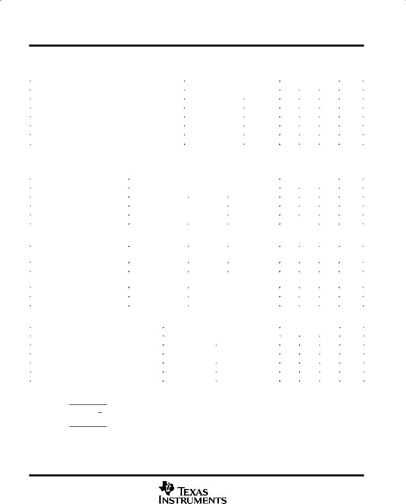
functional block diagram
|
|
|
|
OUTPUT CTRL |
|
|
|
|
|
|
(see Function Table) |
|
|
|
|
|
|
13 |
|
|
RT |
6 |
|
Oscillator |
|
|
|
5 |
|
|
|
|||
CT |
|
8 |
|
|||
|
|
|
||||
|
|
|
C1 |
|||
|
|
|
DTC |
1D |
||
|
|
|
9 |
|
||
≈ 0.1 V |
Comparator |
E1 |
||||
|
||||||
|
|
|||||
DTC |
4 |
|
|
C1 |
|
|
|
|
|
PWM |
11 |
C2 |
|
|
1 |
Error Amplifier 1 Comparator |
|
|||
IN+ |
|
+ |
10 |
E2 |
||
|
|
|||||
|
|
|
||||
|
2 |
|
1 |
Pulse-Steering |
||
IN± |
|
|
||||
|
|
± |
Flip-Flop |
|
||
|
|
|
|
|
||
|
|
Error Amplifier 2 |
12 |
VCC |
||
|
16 |
Undervoltage |
||||
IN+ |
|
+ |
|
|||
|
|
Lockout |
|
|||
IN± |
15 |
|
2 |
Control |
|
|
|
± |
|
||||
|
|
|
|
Reference |
|
|
|
|
|
|
Regulator |
|
|
|
|
|
|
14 |
REF |
|
|
|
|
|
|
||
FEEDBACK |
3 |
|
|
7 |
GND |
|
|
|
|
0.7 mA |
|
|
|
2 |
POST OFFICE BOX 655303 •DALLAS, TEXAS 75265 |
TL594
PULSE-WIDTH-MODULATION CONTROL CIRCUITS
SLVS052C ± APRIL 1988 ± REVISED JULY 1999
absolute maximum ratings over operating free-air temperature range (unless otherwise noted)²
|
|
|
TL594X |
UNIT |
|
|
|
|
|
|
|
Supply voltage, VCC (see Note 1) |
|
|
41 |
V |
|
Amplifier input voltage |
|
|
VCC+0.3 |
V |
|
Collector output voltage |
|
|
41 |
V |
|
|
|
|
|
|
|
Collector output current |
|
|
250 |
mA |
|
|
|
|
|
|
|
Package thermal impedance, θJA |
(see Notes 2 and 3) |
D package |
73 |
°C |
|
|
|
||||
N package |
88 |
||||
|
|
|
|||
|
|
|
|
||
Lead temperature 1,6 mm (1/16 inch) from case for 10 seconds |
260 |
°C |
|||
Storage temperature range, Tstg |
|
|
±65 to 150 |
°C |
|
²Stresses beyond those listed under ªabsolute maximum ratingsº may cause permanent damage to the device. These are stress ratings only, and functional operation of the device at these or any other conditions beyond those indicated under ªrecommended operating conditionsº is not implied. Exposure to absolute-maximum-rated conditions for extended periods may affect device reliability.
NOTES: 1. All voltage values, except differential voltages, are with respect to the network ground terminal.
2.Maximum power dissipation is a function of TJ(max), θJA, and TA. The maximum allowable power dissipation at any allowable ambient temperature is PD = (TJ(max) ± TA)/θJA. Operating at the absolute maximum TJ of 150°C can impact reliability.
3.The package thermal impedance is calculated in accordance with JESD 51, except for through-hole packages, which use a trace length of zero.
recommended operating conditions
|
|
MIN |
MAX |
UNIT |
|
|
|
|
|
|
|
Supply voltage, VCC |
|
7 |
40 |
V |
|
Amplifier input voltage, VI |
|
±0.3 |
VCC±2 |
V |
|
Collector output voltage, VO |
|
|
40 |
V |
|
Collector output current (each transistor) |
|
|
200 |
mA |
|
|
|
|
|
|
|
Current into feedback terminal |
|
|
0.3 |
mA |
|
|
|
|
|
|
|
Timing capacitor, CT |
|
0.47 |
10000 |
nF |
|
Timing resistor, RT |
|
1.8 |
500 |
kΩ |
|
Oscillator frequency, fosc |
|
1 |
300 |
kHz |
|
Operating free-air temperature, TA |
TL594C |
0 |
70 |
°C |
|
TL594I |
±40 |
85 |
°C |
||
|
|||||
|
|
|
|
|
POST OFFICE BOX 655303 •DALLAS, TEXAS 75265 |
3 |
PARAMETER |
TEST CONDITIONS² |
TL594C, TL594I |
UNIT |
||||
|
|
|
|||||
MIN |
TYP³ |
MAX |
|||||
|
|
|
|
||||
Output voltage (REF) |
IO = 1 mA, |
TA = 25°C |
4.95 |
5 |
5.05 |
V |
|
Input regulation |
VCC = 7 V to 40 V, |
TA = 25°C |
|
2 |
25 |
mV |
|
Output regulation |
IO = 1 to 10 mA, |
TA = 25°C |
|
14 |
35 |
mV |
|
Output-voltage change with temperature |
TA = MIN to MAX |
|
|
2 |
10 |
mV/V |
|
Short-circuit output current§ |
V = 0 |
|
10 |
35 |
50 |
mA |
|
|
ref |
|
|
|
|
|
|
² For conditions shown as MIN or MAX, use the appropriate value specified under recommended operating conditions. |
|
|
|||||
³ All typical values except for parameter changes with temperature are at T = 25°C. |
|
|
|
|
|
||
§ Duration of the short circuit should not exceed one second. |
A |
|
|
|
|
|
|
|
|
|
|
|
|
||
amplifier section (see Figure 1)
PARAMETER |
|
TEST CONDITIONS |
|
TL594C, TL594I |
UNIT |
||||||
|
|
|
|
|
|||||||
|
MIN |
TYP³ |
MAX |
||||||||
|
|
|
|
|
|
|
|
|
|||
Input offset voltage, error amplifier |
FEEDBACK = 2.5 V |
|
|
|
|
|
|
2 |
10 |
mV |
|
|
|
|
|
|
|
|
|
|
|
|
|
Input offset current |
FEEDBACK = 2.5 V |
|
|
|
|
|
|
25 |
250 |
nA |
|
|
|
|
|
|
|
|
|
|
|
|
|
Input bias current |
FEEDBACK = 2.5 V |
|
|
|
|
|
|
0.2 |
1 |
µA |
|
|
|
|
|
|
|
|
|
|
|
|
|
Common-mode input voltage range, |
|
|
|
|
|
|
|
0.3 |
|
|
|
VCC = 7 V to 40 V |
|
|
|
|
|
to |
|
|
V |
||
error amplifier |
|
|
|
|
|
|
|
||||
|
|
|
|
|
|
|
VCC±2 |
|
|
||
|
|
|
|
|
|
|
|
|
|
||
Open-loop voltage amplification, error |
VO = 3 V, |
RL = 2 kΩ, |
VO = 0.5 V to 3.5 V |
70 |
95 |
|
dB |
||||
amplifier |
|
||||||||||
|
|
|
|
|
|
|
|
|
|
|
|
|
|
|
|
|
|
|
|
|
|
||
Unity-gain bandwidth |
VO = 0.5 V to 3.5 V, |
RL = 2 kΩ |
|
|
|
800 |
|
kHz |
|||
Common-mode rejection ratio, error |
VCC = 40 V, |
TA = 25°C |
|
|
65 |
80 |
|
dB |
|||
amplifier |
|
|
|
||||||||
|
|
|
|
|
|
|
|
|
|
|
|
|
|
|
|
|
|
|
|
|
|||
Output sink current, FEEDBACK |
VID = ±15 mV to ±5 V, |
FEEDBACK = 0.5 V |
|
0.3 |
0.7 |
|
mA |
||||
Output source current, FEEDBACK |
VID = 15 mV to 5 V, |
FEEDBACK = 3.5 V |
|
±2 |
|
|
mA |
||||
³ All typical values except for parameter changes with temperature are at T |
= 25°C. |
|
|
|
|
|
|||||
|
|
|
|
A |
|
|
|
|
|
|
|
oscillator section, CT = 0.01 µF, RT = 12 kΩ (see Figure 2) |
|
|
|
|
|
|
|
||||
PARAMETER |
|
|
TEST CONDITIONS² |
TL594C, TL594I |
UNIT |
||||||
|
|
|
|
|
|||||||
|
|
MIN |
TYP³ |
MAX |
|||||||
|
|
|
|
|
|
|
|
|
|||
Frequency |
|
|
|
|
|
|
|
|
10 |
|
kHz |
|
|
|
|
|
|
|
|
|
|||
Standard deviation of frequency¶ |
|
All values of V |
CC |
, C , R , and T constant |
|
100 |
|
Hz/kHz |
|||
|
|
|
|
T |
T |
A |
|
|
|
|
|
Frequency change with voltage |
|
VCC = 7 V to 40 V, |
TA = 25°C |
|
1 |
|
Hz/kHz |
||||
Frequency change with temperature# |
|
T = MIN to MAX |
|
|
|
|
50 |
Hz/kHz |
|||
|
|
A |
|
|
|
|
|
|
|
|
|
² For conditions shown as MIN or MAX, use the appropriate value specified under recommended operating conditions. |
|
|
|||||||||
³ All typical values except for parameter changes with temperature are at T |
= 25°C. |
|
|
|
|
|
|||||
|
|
|
|
A |
|
|
|
|
|
|
|
¶ Standard deviation is a measure of the statistical distribution about the mean as derived from the formula:
 Loading...