


Texas Instruments TLC32046MJB, TLC32046MJ, TLC32046MFKB, TLC32046IFN, TLC32046IN Datasheet
...TLC32046C, TLC32046I, TLC32046M
Data Manual
Wide-Band Analog Interface Circuit
SLAS028
May 1995

IMPORTANT NOTICE
Texas Instruments (TI) reserves the right to make changes to its products or to discontinue any semiconductor product or service without notice, and advises its customers to obtain the latest version of relevant information to verify, before placing orders, that the information being relied on is current.
TI warrants performance of its semiconductor products and related software to the specifications applicable at the time of sale in accordance with TI's standard warranty. Testing and other quality control techniques are utilized to the extent TI deems necessary to support this warranty. Specific testing of all parameters of each device is not necessarily performed, except those mandated by government requirements.
Certain applications using semiconductor products may involve potential risks of death, personal injury, or severe property or environmental damage (ªCritical Applicationsº).
TI SEMICONDUCTOR PRODUCTS ARE NOT DESIGNED, INTENDED, AUTHORIZED, OR WARRANTED TO BE SUITABLE FOR USE IN LIFE-SUPPORT APPLICATIONS, DEVICES OR SYSTEMS OR OTHER CRITICAL APPLICATIONS.
Inclusion of TI products in such applications is understood to be fully at the risk of the customer. Use of TI products in such applications requires the written approval of an appropriate TI officer. Questions concerning potential risk applications should be directed to TI through a local SC sales office.
In order to minimize risks associated with the customer's applications, adequate design and operating safeguards should be provided by the customer to minimize inherent or procedural hazards.
TI assumes no liability for applications assistance, customer product design, software performance, or infringement of patents or services described herein. Nor does TI warrant or represent that any license, either express or implied, is granted under any patent right, copyright, mask work right, or other intellectual property right of TI covering or relating to any combination, machine, or process in which such semiconductor products or services might be or are used.
Copyright 1995, Texas Instruments Incorporated

Contents
Section |
Title |
Page |
1 Introduction . . . . . . . . . . . . . . . . . . . . . . . . . . . . . . . . . . . . . . . . . . . . . . . . . . . . . . . . . . . . . . 1±1
1.1 Features . . . . . . . . . . . . . . . . . . . . . . . . . . . . . . . . . . . . . . . . . . . . . . . . . . . . . . . . . . . . . 1±2
1.2 Functional Block Diagrams . . . . . . . . . . . . . . . . . . . . . . . . . . . . . . . . . . . . . . . . . . . . . 1±3
1.3 Terminal Assignments . . . . . . . . . . . . . . . . . . . . . . . . . . . . . . . . . . . . . . . . . . . . . . . . . 1±6
1.4 Ordering Information . . . . . . . . . . . . . . . . . . . . . . . . . . . . . . . . . . . . . . . . . . . . . . . . . . 1±6
1.5 Terminal Functions . . . . . . . . . . . . . . . . . . . . . . . . . . . . . . . . . . . . . . . . . . . . . . . . . . . . 1±7
2 Detailed Description . . . . . . . . . . . . . . . . . . . . . . . . . . . . . . . . . . . . . . . . . . . . . . . . . . . . . . 2±1
2.1 Internal Timing Configuration . . . . . . . . . . . . . . . . . . . . . . . . . . . . . . . . . . . . . . . . . . . 2±2 2.2 Analog Input . . . . . . . . . . . . . . . . . . . . . . . . . . . . . . . . . . . . . . . . . . . . . . . . . . . . . . . . . 2±4 2.3 A/D Band-Pass Filter, Clocking, and Conversion Timing . . . . . . . . . . . . . . . . . . . . 2±4 2.4 A/D Converter . . . . . . . . . . . . . . . . . . . . . . . . . . . . . . . . . . . . . . . . . . . . . . . . . . . . . . . . 2±4 2.5 Analog Output . . . . . . . . . . . . . . . . . . . . . . . . . . . . . . . . . . . . . . . . . . . . . . . . . . . . . . . . 2±4 2.6 D/A Low-Pass Filter, Clocking, and Conversion Timing . . . . . . . . . . . . . . . . . . . . . 2±4 2.7 D/A Converter . . . . . . . . . . . . . . . . . . . . . . . . . . . . . . . . . . . . . . . . . . . . . . . . . . . . . . . . 2±4 2.8 Serial Port . . . . . . . . . . . . . . . . . . . . . . . . . . . . . . . . . . . . . . . . . . . . . . . . . . . . . . . . . . . 2±5 2.9 Synchronous Operation . . . . . . . . . . . . . . . . . . . . . . . . . . . . . . . . . . . . . . . . . . . . . . . . 2±5
2.9.1 One 16-Bit Word . . . . . . . . . . . . . . . . . . . . . . . . . . . . . . . . . . . . . . . . . . . . . . . 2±5 2.9.2 Two 8-Bit Bytes . . . . . . . . . . . . . . . . . . . . . . . . . . . . . . . . . . . . . . . . . . . . . . . 2±5 2.9.3 Synchronous Operating Frequencies . . . . . . . . . . . . . . . . . . . . . . . . . . . . . 2±6 2.10 Asynchronous Operation . . . . . . . . . . . . . . . . . . . . . . . . . . . . . . . . . . . . . . . . . . . . . . . 2±6 2.10.1 One 16-Bit Word . . . . . . . . . . . . . . . . . . . . . . . . . . . . . . . . . . . . . . . . . . . . . . . 2±6 2.10.2 Two 8-Bit Bytes . . . . . . . . . . . . . . . . . . . . . . . . . . . . . . . . . . . . . . . . . . . . . . . . 2±6 2.10.3 Asynchronous Operating Frequencies . . . . . . . . . . . . . . . . . . . . . . . . . . . . 2±6
2.11Operation of TLC32046C and TLC32046I With Internal Voltage Reference . . . 2±7
2.12Operation of TLC32046C AND TLC32046I With External Voltage Reference . 2±7
2.13 |
Reset . . . . . . . . . . . . . . . . . . . . . . . . . . . . . . . . . . . . . . . . . . . . . . . . . . . . . . . . . . . . . . . |
2±7 |
2.14 |
Loopback . . . . . . . . . . . . . . . . . . . . . . . . . . . . . . . . . . . . . . . . . . . . . . . . . . . . . . . . . . . . |
2±7 |
2.15 |
Communications Word Sequence . . . . . . . . . . . . . . . . . . . . . . . . . . . . . . . . . . . . . . . |
2±8 |
|
2.15.1 Primary DR Word Bit Pattern . . . . . . . . . . . . . . . . . . . . . . . . . . . . . . . . . . . . |
2±8 |
|
2.15.2 Primary DX Word Bit Pattern . . . . . . . . . . . . . . . . . . . . . . . . . . . . . . . . . . . . |
2±9 |
|
2.15.3 Secondary DX Word Bit Pattern . . . . . . . . . . . . . . . . . . . . . . . . . . . . . . . . . |
2±10 |
2.16 |
Reset Function . . . . . . . . . . . . . . . . . . . . . . . . . . . . . . . . . . . . . . . . . . . . . . . . . . . . . . . |
2±10 |
2.17 |
Power-Up Sequence . . . . . . . . . . . . . . . . . . . . . . . . . . . . . . . . . . . . . . . . . . . . . . . . . . |
2±11 |
2.18 |
AIC Register Constraints . . . . . . . . . . . . . . . . . . . . . . . . . . . . . . . . . . . . . . . . . . . . . . . |
2±11 |
2.19 |
AIC Responses to Improper Conditions . . . . . . . . . . . . . . . . . . . . . . . . . . . . . . . . . . |
2±11 |
2.20 |
Operation With Conversion Times Too Close Together . . . . . . . . . . . . . . . . . . . . . |
2±12 |
2.21 |
More Than One Receive Frame Sync Occurring Between Two Transmit |
|
|
Frame Syncs ± Asynchronous Operation . . . . . . . . . . . . . . . . . . . . . . . . . . . . . . . . . |
2±12 |
2.22 |
More Than One Transmit Frame Sync Occurring Between Two Receive |
|
|
Frame Syncs ± Asynchronous Operation . . . . . . . . . . . . . . . . . . . . . . . . . . . . . . . . . |
2±13 |
iii

Section |
Title |
Page |
2.23 |
More than One Set of Primary and Secondary DX Serial Communications |
|
|
Occurring Between Two Receive Frame Syncs ± Asynchronous Operation . . . |
2±13 |
2.24 |
System Frequency Response Correction . . . . . . . . . . . . . . . . . . . . . . . . . . . . . . . . . |
2±14 |
2.25 |
(Sin x)/x Correction . . . . . . . . . . . . . . . . . . . . . . . . . . . . . . . . . . . . . . . . . . . . . . . . . . . |
2±14 |
2.26 |
(Sin x)/x Roll-Off for a Zero-Order Hold Function . . . . . . . . . . . . . . . . . . . . . . . . . . |
2±14 |
2.27 |
Correction Filter . . . . . . . . . . . . . . . . . . . . . . . . . . . . . . . . . . . . . . . . . . . . . . . . . . . . . . |
2±15 |
2.28 |
Correction Results . . . . . . . . . . . . . . . . . . . . . . . . . . . . . . . . . . . . . . . . . . . . . . . . . . . . |
2±15 |
2.29 |
TMS320 Software Requirements . . . . . . . . . . . . . . . . . . . . . . . . . . . . . . . . . . . . . . . . |
2±16 |
3 Specifications . . . . . . . . . . . . . . . . . . . . . . . . . . . . . . . . . . . . . . . . . . . . . . . . . . . . . . . . . . . . 3±1
3.1 Absolute Maximum Ratings Over Operating Free-Air Temperature Range . . . . 3±1 3.2 Recommended Operating Conditions . . . . . . . . . . . . . . . . . . . . . . . . . . . . . . . . . . . . 3±1
3.3Electrical Characteristics Over Recommended Operating Free-Air
Temperature Range, VCC+ = 5 V, VCC ± = ±5 V, VDD = 5 V . . . . . . . . . . . . . . . . . 3±2 3.3.1 Total Device, MSTR CLK Frequency = 5.184 MHz . . . . . . . . . . . . . . . . . 3±2
3.3.2 Power Supply Rejection and Crosstalk Attenuation . . . . . . . . . . . . . . . . . 3±2 3.3.3 Serial Port . . . . . . . . . . . . . . . . . . . . . . . . . . . . . . . . . . . . . . . . . . . . . . . . . . . . 3±2 3.3.4 Receive Amplifier Input . . . . . . . . . . . . . . . . . . . . . . . . . . . . . . . . . . . . . . . . . 3±3 3.3.5 Transmit Filter Output . . . . . . . . . . . . . . . . . . . . . . . . . . . . . . . . . . . . . . . . . . 3±3
3.3.6Receive and Transmit Channel System Distortion, SCF Clock
Frequency = 288kHz . . . . . . . . . . . . . . . . . . . . . . . . . . . . . . . . . . . . . . . . . . . 3±3 3.3.7 Receive Channel Signal-to-Distortion Ratio . . . . . . . . . . . . . . . . . . . . . . . 3±4 3.3.8 Transmit Channel Signal-to-Distortion Ratio . . . . . . . . . . . . . . . . . . . . . . . 3±4 3.3.9 Receive and Transmit Gain and Dynamic Range . . . . . . . . . . . . . . . . . . . 3±4 3.3.10 Receive Channel Band-Pass Filter Transfer Function,
SCF fclock = 288 kHz, Input (IN+ ± IN±) Is A +3-V Sine Wave . . . . . . . 3±5 3.3.11 Receive and Transmit Channel Low-Pass Filter Transfer Function,
SCF fclock = 288 kHz . . . . . . . . . . . . . . . . . . . . . . . . . . . . . . . . . . . . . . . . . . . 3±5
3.4Operating Characteristics Over Recommended Operating Free-Air
Temperature Range, VCC+ = 5 V, VCC ± = ±5 V, VDD = 5 V . . . . . . . . . . . . . . . . . 3±6 3.4.1 Receive and Transmit Noise . . . . . . . . . . . . . . . . . . . . . . . . . . . . . . . . . . . . . . 3±6
3.5 Timing Requirements . . . . . . . . . . . . . . . . . . . . . . . . . . . . . . . . . . . . . . . . . . . . . . . . . . 3±6 3.5.1 Serial Port Recommended Input Signals . . . . . . . . . . . . . . . . . . . . . . . . . . 3±6
3.5.2Serial Port ± AIC Output Signals, CL = 30 pF for SHIFT CLK Output,
CL = 15 pF For All Other Outputs . . . . . . . . . . . . . . . . . . . . . . . . . . . . . . . . |
3±7 |
4 Parameter Measurement Information . . . . . . . . . . . . . . . . . . . . . . . . . . . . . . . . . . . . . . . 4±1
5 Typical Characteristics . . . . . . . . . . . . . . . . . . . . . . . . . . . . . . . . . . . . . . . . . . . . . . . . . . . . 5±1
6 Application Information . . . . . . . . . . . . . . . . . . . . . . . . . . . . . . . . . . . . . . . . . . . . . . . . . . . 6±1
iv

List of Illustrations
Figure |
Title |
Page |
1±1 |
Dual-Word (Telephone Interface) Mode . . . . . . . . . . . . . . . . . . . . . . . . . . . . . . . . |
. . . 1±5 |
1±2 |
Word Mode . . . . . . . . . . . . . . . . . . . . . . . . . . . . . . . . . . . . . . . . . . . . . . . . . . . . . . . . |
. . . 1±5 |
1±3 |
Byte Mode . . . . . . . . . . . . . . . . . . . . . . . . . . . . . . . . . . . . . . . . . . . . . . . . . . . . . . . . . |
. . . 1±5 |
2±1 |
Asynchronous Internal Timing Configuration . . . . . . . . . . . . . . . . . . . . . . . . . . . . |
. . . 2±3 |
2±2 |
Primary and Secondary Communications Word Sequence . . . . . . . . . . . . . . . . |
. . . 2±8 |
2±3 |
DR Word Bit Pattern . . . . . . . . . . . . . . . . . . . . . . . . . . . . . . . . . . . . . . . . . . . . . . . . . |
. . . 2±8 |
2±4 |
Primary DX Word BIt Pattern . . . . . . . . . . . . . . . . . . . . . . . . . . . . . . . . . . . . . . . . . |
. . . 2±9 |
2±5 |
Secondary DX Word BIt Pattern . . . . . . . . . . . . . . . . . . . . . . . . . . . . . . . . . . . . . . . |
. . . 2±10 |
2±6 |
Reset on Power-Up Circuit . . . . . . . . . . . . . . . . . . . . . . . . . . . . . . . . . . . . . . . . . . . |
. . . 2±11 |
2±7 |
Conversion Times Too Close Together . . . . . . . . . . . . . . . . . . . . . . . . . . . . . . . . . |
. . . 2±12 |
2±8 |
More Than One Receive Frame Sync Between Two Transmit Frame Syncs |
. . . 2±13 |
2±9 |
More Than One Transmit Frame Sync Between Two Receive Frame Syncs |
. . . 2±13 |
2±10 |
More Than One Set of Primary and Secondary DX Serial Communications |
|
|
Between Two Receive Frame Syncs . . . . . . . . . . . . . . . . . . . . . . . . . . . . . . . . . . . |
. . . 2±14 |
2±11 |
First-Order Correction Filter . . . . . . . . . . . . . . . . . . . . . . . . . . . . . . . . . . . . . . . . . . |
. . . 2±15 |
4±1 |
IN+ and IN ± Gain Control Circuitry . . . . . . . . . . . . . . . . . . . . . . . . . . . . . . . . . . . . |
. . . 4±1 |
4±2 |
Dual-Word (Telephone Interface) Mode Timing . . . . . . . . . . . . . . . . . . . . . . . . . . |
. . . 4±2 |
4±3 |
Word Timing . . . . . . . . . . . . . . . . . . . . . . . . . . . . . . . . . . . . . . . . . . . . . . . . . . . . . . . . |
. . . 4±2 |
4±4 |
Byte Mode Timing . . . . . . . . . . . . . . . . . . . . . . . . . . . . . . . . . . . . . . . . . . . . . . . . . . . |
. . . 4±3 |
4±5 |
Shift-Clock Timing . . . . . . . . . . . . . . . . . . . . . . . . . . . . . . . . . . . . . . . . . . . . . . . . . . . |
. . . 4±4 |
4±6 |
TMS32010/TMS320C15±TLC32046 Interface Timing . . . . . . . . . . . . . . . . . . . |
. . . 4±4 |
4±7 |
TMS32010/TMS320C15±TLC32046 Interface Circuit . . . . . . . . . . . . . . . . . . . . |
. . . 4±5 |
v

List of Tables
Table |
Title |
Page |
2±1 |
Mode-Selection Function Table . . . . . . . . . . . . . . . . . . . . . . . . . . . . . . . . . . . . . . . . . . |
2±1 |
2±2 Primary DX Serial Communication Protocol . . . . . . . . . . . . . . . . . . . . . . . . . . . . . . . . |
2±1 |
|
2±3 Secondary DX Serial Communication Protocol . . . . . . . . . . . . . . . . . . . . . . . . . . . . . |
2±1 |
|
2±4 AIC Responses to Improper Conditions . . . . . . . . . . . . . . . . . . . . . . . . . . . . . . . . . . . |
2±1 |
|
2±5 (sin x)/x Roll-Off Error . . . . . . . . . . . . . . . . . . . . . . . . . . . . . . . . . . . . . . . . . . . . . . . . . . |
2±1 |
|
2±6 (sin x)/x Correction Table for fs = 8000 Hz and fs = 9600 Hz . . . . . . . . . . . . . . . . . |
2±1 |
|
4±1 |
Gain Control Table . . . . . . . . . . . . . . . . . . . . . . . . . . . . . . . . . . . . . . . . . . . . . . . . . . . . . |
4±1 |
vi

1 Introduction
The TLC32046C, TLC32046I, and TLC32046M wide-band analog interface circuits (AIC) are a complete analog-to-digital and digital-to-analog interface system for advanced digital signal processors (DSPs) similar to the TMS32020, TMS320C25, and TMS320C30. The TLC32046C and TLC32046I offer a powerful combination of options under DSP control: three operating modes (dual-word [telephone interface], word, and byte) combined with two word formats (8 bits and 16 bits) and synchronous or asynchronous operation. It provides a high level of flexibility in that conversion and sampling rates, filter bandwidths, input circuitry, receive and transmit gains, and multiplexed analog inputs are under processor control.
This AIC features a
•band-pass switched-capacitor antialiasing input filter
•14-bit-resolution A/D converter
•14-bit-resolution D/A converter
•low-pass switched-capacitor output-reconstruction filter.
The antialiasing input filter comprises eighth-order and fourth-order CC-type (Chebyshev/elliptic transitional) low-pass and high-pass filters, respectively. The input filter is implemented in switchedcapacitor technology and is preceded by a continuous time filter to eliminate any possibility of aliasing caused by sampled data filtering. When low-pass filtering is desired, the high-pass filter can be switched out of the signal path. A selectable auxiliary differential analog input is provided for applications where more than one analog input is required.
The output-reconstruction filter is an eighth-order CC-type (Chebyshev/elliptic transitional low-pass filter) followed by a second-order (sin x)/x correction filter and is implemented in switched-capacitor technology. This filter is followed by a continuous-time filter to eliminate images of the sample data signal. The on-board (sin x)/x correction filter can be switched out of the signal path using digital signal processor control.
The A/D and D/A architectures ensure no missing codes and monotonic operation. An internal voltage reference is provided to ease the design task and to provide complete control over the performance of the IC. The internal voltage reference is brought out to REF. Separate analog and digital voltage supplies and ground are provided to minimize noise and ensure a wide dynamic range. The analog circuit path contains only differential circuitry to keep noise to a minimum. The exception is the DAC sample-and-hold, which utilizes pseudo-differential circuitry.
The TLC32046C is characterized for operation from 0°C to 70°C, the TLC32046I is characterized for operation from ±40°C to 85°C, and the TLC32046M is characterized for operation from ±55°C to 125°C.
1±1

1.1Features
•14-Bit Dynamic Range ADC and DAC
•16-Bit Dynamic Range Input With Programmable Gain
•Synchronous or Asynchronous ADC and DAC Sampling Rates Up to 25,000 Samples Per Second
•Programmable Incremental ADC and DAC Conversion Timing Adjustments
•Typical Applications
±Speech Encryption for Digital Transmission
±Speech Recognition and Storage Systems
±Speech Synthesis
±Modems at 8-kHz, 9.6-kHz, and 16-kHz Sampling Rates
±Industrial Process Control
±Biomedical Instrumentation
±Acoustical Signal Processing
±Spectral Analysis
±Instrumentation Recorders
±Data Acquisition
•Switched-Capacitor Antialiasing Input Filter and Output-Reconstruction Filter
•Three Fundamental Modes of Operation: Dual-Word (Telephone Interface), Word, and Byte
•600-mil Wide N Package
•Digital Output in Twos Complement Format
•CMOS Technology
FUNCTION TABLE
DATA |
SYNCHRONOUS |
ASYNCHRONOUS |
|
|
|
(CONTROL |
(CONTROL |
|
DIRECT |
||
COMMUNICATIONS |
FORCING CONDITION |
||||
REGISTER |
REGISTER |
INTERFACE |
|||
FORMAT |
|
||||
BIT D5 = 1) |
BIT D5 = 0) |
|
|
||
|
|
|
|||
|
|
|
|
|
|
16-bit format |
Dual-word |
Dual-word |
Terminal 13 = 0 to 5 V |
TMS32020, |
|
|
(telephone |
(telephone interface) |
Terminal 1 = 0 to 5 V |
TMS320C25, |
|
|
interface) mode |
mode |
|
TMS320C30 |
|
|
|
|
|
|
|
16-bit format |
Word mode |
Word mode |
Terminal 13 = VCC± (± 5 V nom) |
TMS32020, |
|
|
|
|
Terminal 1 = VCC+ (5 V nom) |
TMS320C25, |
|
|
|
|
|
TMS320C30, |
|
|
|
|
|
indirect |
|
|
|
|
|
interface to |
|
|
|
|
|
TMS320C10. |
|
|
|
|
|
(see Figure 7). |
|
|
|
|
|
|
|
8-bit format |
Byte mode |
Byte mode |
Terminal 13 = VCC ± (± 5 V nom) |
TMS320C17 |
|
(2 bytes required) |
|
|
Terminal 1 = VCC ± (± 5 V nom) |
|
1±2

1.2Functional Block Diagrams
WORD OR BYTE MODE
IN + 26 |
|
|
|
|
|
|
|
|
|
|
IN ± |
25 |
M |
Low-Pass |
|
M |
|
Serial |
5 |
DR |
|
24 |
U |
|
U |
A/D |
||||||
AUX IN + |
|
X |
|
Filter |
|
X |
|
Port |
4 |
|
AUX IN ± 23 |
|
|
|
|
|
FSR |
||||
|
|
|
|
|
|
|
3 |
|||
|
|
|
|
|
|
|
|
|
EODR |
|
|
|
|
High-Pass |
|
|
|
|
|
||
|
|
|
|
|
|
|
6 |
MSTR CLK |
||
|
Receive Section |
|
Filter |
|
|
|
|
|
||
|
|
|
|
|
|
10 SHIFT CLK |
||||
|
|
|
|
|
|
|
Internal |
|
||
|
|
|
|
|
|
|
|
1 WORD- |
||
|
|
|
|
|
|
|
Voltage |
|
||
|
|
|
|
|
|
|
Reference |
|
|
BYTE |
|
Transmit Section |
|
|
|
|
|
13 CONTROL |
|||
|
|
|
|
|
|
|
||||
|
|
|
|
|
|
|
|
|
12 |
DX |
|
|
|
|
|
|
|
|
|
|
|
|
22 |
|
|
|
|
|
|
|
14 |
FSX |
OUT + |
|
Low-Pass |
|
|
|
|
11 |
|||
|
|
M |
(sin x)/x |
D/A |
|
EODX |
||||
OUT ± |
|
|
Filter |
|
Correction |
|
|
|||
21 |
|
|
U |
|
|
|
|
|||
|
|
|
|
|
|
|
|
|
||
|
|
|
|
X |
|
|
|
|
|
|
|
|
|
|
|
|
|
|
|
|
|
|
20 |
19 |
17,18 |
9 |
|
7 |
8 |
2 |
|
|
|
VCC + |
VCC ± |
ANLG |
DGTL |
|
VDD |
REF |
RESET |
|
|
|
|
|
GND |
GND |
(DIGITAL) |
|
|
|
|
|
DUAL-WORD (TELEPHONE INTERFACE) MODE
IN + 26 |
|
|
|
|
|
|
|
|
25 |
M |
|
|
|
M |
|
Serial |
5 |
IN ± 24 |
U |
Low-Pass |
|
U |
A/D |
|||
|
DR |
|||||||
AUX IN + |
X |
Filter |
|
X |
|
Port |
4 |
|
23 |
|
|
|
|
|
|||
AUX IN ± |
|
|
|
|
|
|
|
FSR |
|
|
|
|
|
|
|
|
3 |
|
|
|
|
|
|
|
|
D11 OUT |
|
|
High-Pass |
|
|
|
|
6 |
|
Receive Section |
Filter |
|
|
|
|
MSTR CLK |
||
|
|
|
|
10 |
||||
|
|
|
|
|
|
|||
|
|
|
|
|
|
Internal |
|
SHIFT CLK |
|
|
|
|
|
|
|
1 |
|
|
|
|
|
|
|
Voltage |
|
|
|
|
|
|
|
|
|
FSD |
|
|
|
|
|
|
|
Reference |
|
|
|
|
|
|
|
|
|
13 |
|
Transmit Section |
|
|
|
|
|
|
DATA DR |
|
|
|
|
|
|
|
12 |
||
|
|
|
|
|
|
|
|
|
|
|
|
|
|
|
|
|
DX |
|
|
|
|
|
|
|
|
14 |
22 |
|
|
|
|
|
|
|
FSX |
OUT + |
|
Low-Pass |
|
M |
(sin x)/x |
D/A |
|
11 |
OUT ± |
|
Filter |
|
Correction |
|
D10 OUT |
||
|
|
U |
|
|
|
|||
21 |
|
|
|
|
|
|
|
|
|
|
|
X |
|
|
|
|
|
|
|
|
|
|
|
|
|
|
20 |
19 |
17,18 |
9 |
|
7 |
8 |
2 |
|
VCC + |
VCC ± |
ANLG |
DGTL |
|
VDD |
REF |
RESET |
|
|
|
GND |
GND |
(DIGITAL) |
|
|
|
|
|
|
|
|
|
|
|
|
1±3 |
FRAME SYNCHRONIZATION FUNCTIONS
Function |
|
|
Frame Sync Output |
||
|
|
|
|
||
Receiving serial data on DX from processor to internal DAC |
|
|
|
|
low |
|
|
FSX |
|
||
|
|
|
|||
Transmitting serial data on DR from internal ADC to processor, primary communications |
|
|
|
|
low |
|
FSR |
||||
|
|
|
|||
Transmitting serial data on DR from Data-DR to processor, secondary communications in |
|
|
|||
|
|
FSD |
low |
||
dual-word (telephone interface) mode only |
|
|
|
|
|
|
|
|
|
|
|
Analog In
Analog Out
|
|
5 V |
± 5 V |
|
|
|
||||
20 |
|
19 |
|
|
|
|
||||
|
|
|
|
|
||||||
26 |
|
VCC + |
VCC ± |
|||||||
IN + |
|
|
|
DR |
||||||
25 |
|
|
|
|||||||
IN ± |
|
|
|
|
|
|||||
|
TLC32046 |
|
|
|
||||||
FSR |
||||||||||
|
|
|
|
|
||||||
|
|
|
|
|
|
|
||||
|
|
|
|
|
D11OUT |
|||||
22 |
OUT + |
|
|
|
|
|
||||
|
|
|
|
DX |
||||||
21 |
|
|
|
|
|
|
|
|||
OUT ± |
|
|
|
|
|
|||||
|
|
|
|
|
|
|||||
|
|
|
|
|
|
|
|
|
||
|
|
|
|
|
|
|
|
FSX |
|
|
|
|
|
|
|
D10OUT |
|||||
1 |
|
|
|
|
|
|
|
|
|
|
FSD |
DATA-DR |
|||||||||
|
||||||||||
|
|
|
|
|
||||||
|
|
|
|
|
|
|
|
|
|
|
Serial Data Out
5 |
|
|
|
|
|
|
|
4 |
|
|
|
3 |
|
|
TMS32020, |
|
|
|
|
|
|
|
TMS320C25, |
|
|
|
|
12 |
Serial Data In |
|
TMS320C30, or |
|
|||
|
Equivalent 16-Bit DSP |
||
|
|
|
|
14 |
|
|
TTL or CMOS |
11 |
|
|
Logic Levels |
|
|
|
|
|
|
|
|
Secondary Communication (see Table above) 13 Serial Data Input
16-Bit Format TTL
or CMOS Logic Levels
Figure 1±1. Dual-Word (Telephone Interface) Mode
When the DATA-DR/CONTROL input is tied to a logic signal source varying between 0 and 5 V, the TLC32046 is in the dual-word (telephone interface) mode. This logic signal is routed to the DR line for input to the DSP only when data frame synchronization (FSD) outputs a low level. The FSD pulse duration is 16 shift clock pulses. Also, in this mode, the control register data bits D10 and D11 appear on D10OUT and D11OUT, respectively, as outputs.
1±4
|
|
5 V |
|
± 5 V |
|
|
|
|||||||
|
|
20 |
|
|
19 |
|
|
|
|
|
|
|
|
|
|
|
|
|
|
|
|
|
|
|
|
|
|
||
|
26 |
VCC + |
|
VCC ± |
5 |
Serial Data Out |
||||||||
|
|
|
|
|
|
|
|
|
DR |
|||||
Analog In |
25 |
IN + |
|
|
|
|
|
|
|
|
|
|||
IN ± |
TLC32046 |
|
|
|
|
|
|
4 |
|
|
||||
|
|
|
|
|
|
|
|
|
|
|||||
|
|
|
|
|
FSR |
|
|
|||||||
|
|
|
|
|
|
|
|
|
|
|
|
|||
|
|
|
|
|
|
|
|
|
|
|
|
3 |
|
TMS32020, |
|
|
|
|
|
|
EODR |
||||||||
|
|
|
|
|
|
|
|
TMS320C25, |
||||||
|
|
|
|
|
|
|
|
|
|
|
|
|
|
|
|
22 |
OUT + |
|
|
|
|
|
|
|
|
12 |
Serial Data In |
TMS320C30, |
|
Analog Out |
|
|
|
|
|
|
DX |
or Equivalent |
||||||
|
|
|
|
|
|
|
||||||||
21 |
OUT ± |
|
|
|
|
|
|
|
|
16-Bit DSP |
||||
|
|
|
|
|
|
|
|
|
|
|
|
|||
|
|
|
|
|
|
|
|
|
|
14 |
|
|
||
|
|
|
|
|
|
|
|
|
|
|
|
|
TTL or CMOS |
|
|
|
|
|
|
|
|
|
|
FSX |
|||||
|
|
|
|
|
|
|
|
|
|
|
Logic Levels |
|||
|
|
|
|
|
|
|
|
|
|
|
|
|
|
|
|
|
|
|
|
|
|
|
|
|
|
|
11 |
|
|
|
|
|
|
|
|
|
|
EODX |
|
|
||||
|
|
|
|
|
|
|
|
|
|
|
||||
VCC+ |
|
|
|
|
|
|
|
|
|
|
|
|
VCC ± |
|
(5 V nom) |
1 |
WORD-BYTE |
|
|
|
|
|
|
|
13 |
(± 5 V nom) |
|||
|
CONTROL |
|
|
|||||||||||
|
|
|
|
|
|
|
|
|||||||
|
|
|
|
|
|
|
|
|
|
|
|
|
|
|
|
|
|
|
Figure 1±2. Word Mode |
|
||||||||||
|
|
5 V |
|
± 5 V |
|
|
|
|
|||||||
|
|
20 |
|
|
19 |
|
|
|
|
|
|
|
|
|
|
|
|
|
|
|
|
|
|
|
|
|
|
|
|
||
|
26 |
VCC + |
|
VCC ± |
5 |
Serial Data Out |
|
||||||||
|
|
|
|
|
|
|
|
|
DR |
|
|||||
Analog In |
25 |
IN + |
|
|
|
|
|
|
|
|
|
|
|||
IN ± |
|
|
|
|
|
|
|
|
4 |
|
|
|
|||
|
|
TLC32046 |
|
|
|
|
|
|
|
|
|||||
|
|
|
FSR |
|
|
|
|||||||||
|
|
|
|
|
|
|
|
|
|
|
|
||||
|
|
|
|
|
|
|
|
|
|
|
|
3 |
|
|
TMS320C17 or |
|
|
|
|
|
|
|
EODR |
|
|
||||||
|
|
|
|
|
|
|
|
|
|
||||||
|
22 |
|
|
|
|
|
|
|
|
|
|
|
|
|
Equivalent |
|
|
|
|
|
|
|
|
|
|
|
|
|
|
||
|
OUT+ |
|
|
|
|
|
|
|
|
12 |
Serial Data In |
|
8-Bit Serial Interface |
||
|
|
|
|
|
|
|
|
|
|
||||||
Analog Out |
|
|
|
|
|
|
|
DX |
|
(2 bytes required) |
|||||
|
|
|
|
|
|
|
|
|
|
|
|
||||
21 |
|
|
|
|
|
|
|
|
|
|
|
|
|||
|
OUT± |
|
|
|
|
|
|
|
|
|
|
|
|
||
|
|
|
|
|
|
|
|
|
|
14 |
|
|
TTL or CMOS |
||
|
|
|
|
|
|
|
|
|
|
|
|
|
|
||
|
|
|
|
|
|
|
|
|
FSX |
|
|
||||
|
|
|
|
|
|
|
|
|
|
|
|
Logic Levels |
|||
|
|
|
|
|
|
|
|
|
|
|
|
|
|
|
|
|
|
|
|
|
|
|
|
|
|
|
|
11 |
|
|
|
VCC ± |
|
|
|
|
|
|
|
EODX |
|
|
|
||||
|
|
|
|
|
|
|
|
|
|
|
|||||
|
|
|
|
|
|
|
VCC ± |
|
|||||||
|
|
|
|
|
|
|
|
|
|
|
|
|
|||
(± 5 V nom) |
1 |
WORD-BYTE |
|
|
|
|
|
|
|
13 |
(± 5 V nom) |
||||
|
CONTROL |
||||||||||||||
|
|
|
|
|
|
||||||||||
|
|
|
|
|
|
|
|
|
|||||||
|
|
|
|
|
|
|
|
|
|
|
|
|
|
|
|
Figure 1±3. Byte Mode
The word or byte mode is selected by first connecting the DATA-DR/CONTROL input to VCC±. FSD/WORD-BYTE becomes an input and can then be used to select either word or byte transmission
formats. The end-of-data transmit (EODX) and the end-of-data receive (EODR) signals respectively, are used to signal the end of word or byte communication (see the Terminal Functions section).
1±5

1.3Terminal Assignments
|
|
|
|
J ² OR N PACKAGE ³ |
|
|
|
|
FK OR FN PACKAGE |
|
||||||||||||||||||||||||
|
|
|
|
|
|
|
|
|
(TOP VIEW) |
|
|
|
|
|
|
|
|
(TOP VIEW) |
|
|
|
|
||||||||||||
|
|
|
|
|
|
|
|
|
|
|
|
|
|
|
|
|
|
|
|
|
|
|
|
|
|
|
|
|
|
|
|
|
||
|
|
|
|
|
|
|
|
|
|
|
|
|
|
|
|
|
|
§ |
|
|
|
|
§ |
|
|
|
|
|
|
|
|
|
||
|
|
|
|
|
|
|
|
|
|
|
|
|
|
|
|
|
|
|
|
|
|
|
|
|
|
|
|
|
|
|||||
|
|
MSTR CLK |
|
6 |
23 |
AUX IN ± |
|
|
|
|
|
FSR |
|
D11OUOT/EODR |
|
RESET |
|
FSD/WORD-BYTE |
NU NU |
IN+ |
|
|||||||||||||
FSD/WORD-BYTE§ |
|
1 |
28 |
NU |
|
|
|
|
|
|
|
|
|
|
|
|
|
|
|
|
|
|
|
|
|
|
|
|||||||
|
|
|
RESET |
|
|
2 |
27 |
NU |
|
|
|
|
|
|
|
|
|
|
|
|
|
|
|
|
|
|
|
|
|
|
|
|||
|
D11OUT/EODR |
§ |
|
3 |
26 |
IN+ |
|
|
|
|
|
|
|
|
|
|
|
|
|
|
|
|
|
|
|
|
|
|
|
|||||
|
|
|
|
FSR |
|
|
|
4 |
25 |
IN ± |
|
|
|
|
|
|
|
|
|
|
|
|
|
|
|
|
|
|
|
|
|
|
|
|
|
|
|
|
|
|
|
|
|
|
|
|
|
|
|
|
|
|
|
|
|
|
|
|
|
|
|
|
|
|
|||||
|
|
|
|
DR |
|
5 |
24 |
AUX IN+ |
|
|
|
|
|
|
|
|
|
|
|
|
|
|
|
|
|
|
|
|
|
|
|
|||
|
|
|
|
|
|
|
|
|
|
|
|
|
|
|
|
|
|
|
|
|
|
|
|
|
|
|
|
|||||||
|
|
|
VDD |
|
7 |
22 |
OUT+ |
|
|
|
|
|
|
|
|
|
|
|
|
|
|
|
|
|
|
|
|
|
|
|
||||
|
|
|
|
|
|
|
|
|
|
|
|
|
|
|
|
|
|
|
|
|
|
|
|
|
|
|
||||||||
|
|
|
|
|
|
|
|
|
|
|
|
|
|
|
|
|
|
|
|
|
|
|
|
|
|
|
||||||||
|
|
|
|
|
|
|
|
4 |
3 |
|
2 |
|
1 |
|
28 27 26 |
|
|
|
||||||||||||||||
|
|
|
|
|
|
|
|
|
|
|
|
|
|
|
|
|
|
|
|
|
|
|||||||||||||
|
|
|
|
REF |
|
8 |
21 |
OUT± |
|
DR |
|
5 |
|
|
|
|
|
|
|
|
|
|
|
|
|
|
25 |
|
IN ± |
|||||
|
|
DGTL GND |
|
9 |
20 |
VCC+ |
MSTR CLK |
|
6 |
|
|
|
|
|
|
|
|
|
|
|
|
|
|
24 |
|
AUX IN+ |
||||||||
|
|
SHIFT CLK |
|
10 |
19 |
VCC ± |
|
VDD |
|
7 |
|
|
|
|
|
|
|
|
|
|
|
|
|
|
23 |
|
AUX IN ± |
|||||||
|
|
|
|
|
§ |
|
|
|
ANLG GND |
|
REF |
|
|
|
|
|
|
|
|
|
|
|
|
|
|
|
|
|
|
|
|
|||
|
D10OUT/EODX |
|
11 |
18 |
|
|
8 |
|
|
|
|
|
|
|
|
|
|
|
|
|
|
22 |
|
OUT+ |
||||||||||
|
|
|
|
DX |
|
12 |
17 |
ANLG GND |
DGTL GND |
|
9 |
|
|
|
|
|
|
|
|
|
|
|
|
|
|
21 |
|
OUT± |
||||||
DATA-DR/CONTROL§ |
|
13 |
16 |
NU |
SHIFT CLK |
|
10 |
|
|
|
|
|
|
|
|
|
|
|
|
|
20 |
|
VCC+ |
|||||||||||
|
|
|
|
|
|
|
|
|
NU |
|
|
§ |
|
|
|
|
|
|
|
|
|
|
|
|
|
|
|
|
|
|
|
|
||
|
|
|
|
FSX |
|
|
14 |
15 |
D10OUT/EODX |
|
11 |
|
|
|
|
|
|
|
|
|
|
|
|
|
19 |
|
VCC ± |
|||||||
|
|
|
|
|
|
|
|
|
|
|
|
|
|
|
12 13 14 15 16 1718 |
|
|
|
||||||||||||||||
|
|
|
|
|
|
|
|
|
|
|
|
|
|
|
|
|
|
|
|
|
|
|
|
|
|
|
|
|
|
|
|
|
|
|
|
|
|
|
|
|
|
|
|
|
|
|
|
|
|
|
|
|
|
|
|
|
|
|
|
|
|
|
|
|
|
|
|
|
|
|
|
|
|
|
|
|
|
|
|
|
|
|
|
|
|
|
DX |
§ |
|
|
FSX |
NU |
NU ANLG GND |
ANLG GND |
|
|||||||||
|
|
|
|
|
|
|
|
|
|
|
|
|
|
|
|
|
|
|
|
|||||||||||||||
|
|
|
|
|
|
|
|
|
|
|
|
|
|
|
|
|
|
DR/CONTROL |
|
|
||||||||||||||
|
|
|
|
|
|
|
|
|
|
|
|
|
|
|
|
|
|
|
|
|
|
|
|
|||||||||||
|
|
|
|
|
|
|
|
|
|
|
|
|
|
|
|
|
|
|
DATA- |
|
|
|
|
|
|
|
|
|
|
|
|
|
|
|
NU - Nonusable; no external connection should be made to these terminals.
² Refer to the mechanical data for the JT package. ³ 600-mil wide
§The portion of the terminal name to the left of the slash is used for the dual-word (telephone interface) mode. The portion of the terminal name to the right of the slash is used for word-byte mode.
1.4Ordering Information
AVAILABLE OPTIONS
|
|
PACKAGE |
|
||
|
|
|
|
|
|
TA |
PLASTIC CHIP |
PLASTIC DIP |
CERAMIC DIP |
CHIP CARRIER |
|
CARRIER |
|||||
|
(N) |
(J) |
(FK) |
||
|
(FN) |
||||
|
|
|
|
||
|
|
|
|
|
|
0°C to 70°C |
TLC32046CFN |
TLC32046CN |
|
|
|
|
|
|
|
|
|
± 40°C to 85°C |
TLC32046IFN |
TLC32046IN |
|
|
|
|
|
|
|
|
|
± 55°C to 125°C |
|
|
TLC32046MJ |
TLC32046MFK |
|
1±6

1.5Terminal Functions
|
TERMINAL |
I/O |
DESCRIPTION |
||||||
|
NAME |
NO. |
|||||||
|
|
|
|
|
|
||||
|
|
|
|
|
|
|
|
|
|
ANLG GND |
17,18 |
|
Analog ground return for all internal analog circuits. Not internally connected to DGTL |
||||||
|
|
|
|
|
|
GND. |
|||
|
|
|
|
|
|
|
|
|
|
AUX IN + |
24 |
I |
Noninverting auxiliary analog input stage. AUX IN+ can be switched into the band-pass |
||||||
|
|
|
|
|
|
filter and ADC path via software control. If the appropriate bit in the control register is |
|||
|
|
|
|
|
|
a 1, the auxiliary inputs replace the IN + and IN ± inputs. If the bit is a 0, the IN + and IN ± |
|||
|
|
|
|
|
|
inputs are used (see the DX Serial Data Word Format). |
|||
|
|
|
|
|
|
|
|
|
|
AUX IN ± |
23 |
I |
Inverting auxiliary analog input (see the above AUX IN + description). |
||||||
|
|
|
|
|
|
|
|
|
|
DATA-DR |
13 |
I |
The dual-word (telephone interface) mode, selected by applying an input logic level |
||||||
|
|
|
|
|
|
between 0 and 5 V to DATA-DR, allows this terminal to function as a data input. The data |
|||
|
|
|
|
|
|
is then framed by the FSD signal and transmitted as an output to the DR line during |
|||
|
|
|
|
|
|
secondary communication. The functions FSD, D11OUT, and D10OUT are valid with |
|||
|
|
|
|
|
|
this mode selection (see Table 2±1). |
|||
CONTROL |
|
|
When CONTROL is tied to VCC ±, the device is in the word or byte mode. The functions |
||||||
|
|
|
|
|
|
WORD-BYTE, EODR, and EODX are valid in this mode. CONTROL is then used to |
|||
|
|
|
|
|
|
select either the word or byte mode (see Function Table). |
|||
|
|
|
|
|
|
|
|
|
|
DR |
5 |
O |
DR is used to transmit the ADC output bits from the AIC to the TMS320 serial port. This |
||||||
|
|
|
|
|
|
transmission of bits from the AIC to the TMS320 serial port is synchronized with |
|||
|
|
|
|
|
|
SHIFT CLK. |
|||
|
|
|
|
|
|
|
|
|
|
DX |
12 |
I |
DX is used to receive the DAC input bits and timing and control information from the |
||||||
|
|
|
|
|
|
TMS320. This serial transmission from the TMS320 serial port is synchronized with |
|||
|
|
|
|
|
|
SHIFT CLK. |
|||
|
|
|
|
|
|
|
|
|
|
D10OUT |
11 |
O |
In the dual-word (telephone interface) mode, bit D10 of the control register is output to |
||||||
|
|
|
|
|
|
D10OUT. When the device is reset, bit D10 is initialized to 0 (see DX Serial Data Word |
|||
|
|
|
|
|
|
Format). The output update is immediate upon changing bit D10. |
|||
|
|
|
|
End-of-data transmit. During the word-mode timing, a low-going pulse occurs on |
|
|
|||
|
EODX |
|
|
|
|
EODX |
|
||
|
|
|
|
|
|
immediately after the 16 bits of DAC and control or register information have transmitted |
|||
|
|
|
|
|
|
from the TMS320 serial port to the AIC.This signal can be used to interrupt a |
|||
|
|
|
|
|
|
microprocessor upon completion of serial communications. Also, this signal can be |
|||
|
|
|
|
|
|
used to strobe and enable external serial-to-parallel shift registers, latches, or external |
|||
|
|
|
|
|
|
FIFO RAM and to facilitate parallel data bus communications between the DSP and the |
|||
|
|
|
|
|
|
serial-to-parallel shift registers. During the byte-mode timing, this signal goes low after |
|||
|
|
|
|
|
|
the first byte has been transmitted from the TMS320 serial port to the AIC and is kept |
|||
|
|
|
|
|
|
low until the second byte has been transmitted. The TMS320C17 can use this low-going |
|||
|
|
|
|
|
|
signal to differentiate first and second bytes. |
|||
|
|
|
|
|
|
||||
D11OUT |
3 |
O |
In the dual-word (telephone interface) mode, bit D11 of the control register is output to |
||||||
|
|
|
|
|
|
D11OUT. When the device is reset, bit D11 is initialized to 0 (see DX Serial Data Word |
|||
|
|
|
|
|
|
Format). The output update is immediate upon changing bit D11. |
|||
|
|
|
End-of-data receive. During the word-mode timing, a low-going pulse occurs on |
|
|||||
|
EODR |
|
|
|
EODR |
|
|||
|
|
|
|
|
|
immediately after the 16 bits of A/D information have been transmitted from the AIC to |
|||
|
|
|
|
|
|
the TMS320 serial port. This signal can be used to interrupt a microprocessor upon |
|||
|
|
|
|
|
|
completion of serial communications. Also, this signal can be used to strobe and enable |
|||
|
|
|
|
|
|
external serial-to-parallel shift registers, latches, or external FIFO RAM, and to facilitate |
|||
|
|
|
|
|
|
parallel data bus communications between the DSP and the serial-to-parallel shift |
|||
|
|
|
|
|
|
registers. During the byte-mode timing, this signal goes low after the first byte has been |
|||
|
|
|
|
|
|
transmitted from the AIC to the TMS320 serial port and is kept low until the second byte |
|||
|
|
|
|
|
|
has been transmitted. The TMS320C17 can use this low-going signal to differentiate |
|||
|
|
|
|
|
|
between first and second bytes. |
|||
|
|
|
|
|
|
|
|
|
|
1±7

1.5Terminal Functions (continued)
|
|
|
|
|
TERMINAL |
|
I/O |
|
|
|
|
DESCRIPTION |
|||||
|
|
NAME |
NO. |
|
|
|
|
||||||||||
|
|
|
|
|
|
|
|
|
|
|
|
||||||
|
|
|
|
|
|
|
|
|
|
|
|
|
|
|
|
|
|
|
DGTL |
9 |
|
Digital ground for all internal logic circuits. Not internally connected to ANLG GND. |
|||||||||||||
|
|
|
|
|
|
|
|
|
|
|
|
|
|
|
|
|
|
|
|
|
|
|
|
|
1 |
O |
Frame sync data. The |
|
|
output remains high during primary communication. In the |
|||||
|
FSD |
|
|
FSD |
|||||||||||||
|
|
|
|
|
|
|
|
|
dual-word (telephone interface) mode, FSD is identical to FSX during secondary |
||||||||
|
|
|
|
|
|
|
|
|
communication. |
||||||||
|
WORD-BYTE |
|
I |
WORD-BYTE allows differentiation between the word and byte data format (see |
|||||||||||||
|
|
|
|
|
|
|
|
|
DATA-DR/CONTROL and Table 2-1 for details). |
||||||||
|
|
|
|
|
|
|
|
|
|
|
|
|
|||||
|
|
|
|
|
|
|
4 |
O |
Frame sync receive. |
|
|
is held low during bit transmission. When |
|
goes low, the |
|||
|
|
FSR |
|
|
FSR |
FSR |
|||||||||||
|
|
|
|
|
|
|
|
|
TMS320 serial port begins receiving bits from the AIC via DR of the AIC. The most |
||||||||
|
|
|
|
|
|
|
|
|
significant DR bit is present on DR before FSR goes low (see Serial Port Sections and |
||||||||
|
|
|
|
|
|
|
|
|
Internal Timing Configuration Diagrams). |
||||||||
|
|
|
|
|
|
|
|
||||||||||
|
|
|
|
|
|
|
14 |
O |
Frame sync transmit. When FSX goes low, the TMS320 serial port begins transmitting |
||||||||
|
|
FSX |
|
|
|||||||||||||
|
|
|
|
|
|
|
|
|
bits to the AIC via DX of the AIC. FSX is held low during bit transmission (see Serial Port |
||||||||
|
|
|
|
|
|
|
|
|
Sections and Internal Timing Configuration Diagrams). |
||||||||
|
|
|
|
|
|
|
|
||||||||||
|
IN+ |
26 |
I |
Noninverting input to analog input amplifier stage |
|||||||||||||
|
|
|
|
|
|
|
|
||||||||||
|
IN ± |
25 |
I |
Inverting input to analog input amplifier stage |
|||||||||||||
|
|
|
|
|
|
|
|
||||||||||
|
MSTR CLK |
6 |
I |
The master clock signal is used to derive all the key logic signals of the AIC, such as |
|||||||||||||
|
|
|
|
|
|
|
|
|
the shift clock, the switched-capacitor filter clocks, and the A/D and D/A timing signals. |
||||||||
|
|
|
|
|
|
|
|
|
The Internal Timing Configuration diagram shows how these key signals are derived. |
||||||||
|
|
|
|
|
|
|
|
|
The frequencies of these signals are synchronous submultiples of the master clock |
||||||||
|
|
|
|
|
|
|
|
|
frequency to eliminate unwanted aliasing when the sampled analog signals are |
||||||||
|
|
|
|
|
|
|
|
|
transferred between the switched-capacitor filters and the ADC and DAC converters |
||||||||
|
|
|
|
|
|
|
|
|
(see the Internal Timing Configuration). |
||||||||
|
|
|
|
|
|
|
|
||||||||||
|
OUT+ |
22 |
O |
Noninverting output of analog output power amplifier. OUT+ drives transformer hybrids |
|||||||||||||
|
|
|
|
|
|
|
|
|
or high-impedance loads directly in a differential or a single-ended configuration. |
||||||||
|
|
|
|
|
|
|
|
||||||||||
|
OUT± |
21 |
O |
Inverting output of analog output power amplifier. OUT± is functionally identical with and |
|||||||||||||
|
|
|
|
|
|
|
|
|
complementary to OUT+. |
||||||||
|
|
|
|
|
|
|
|
||||||||||
|
REF |
8 |
I/O |
The internal voltage reference is brought out on REF. An external voltage reference can |
|||||||||||||
|
|
|
|
|
|
|
|
|
be applied to REF to override the internal voltage reference. |
||||||||
|
|
|
|
|
|
|
|||||||||||
|
|
|
|
|
|
|
2 |
I |
A reset function is provided to initialize TA, TA', TB, RA, RA', RB (see Figure 2-1), and |
||||||||
|
|
RESET |
|
||||||||||||||
|
|
|
|
|
|
|
|
|
the control registers. This reset function initiates serial communications between the |
||||||||
|
|
|
|
|
|
|
|
|
AIC and DSP. The reset function initializes all AIC registers, including the control |
||||||||
|
|
|
|
|
|
|
|
|
register. After a negative-going pulse on RESET, the AIC registers are initialized to |
||||||||
|
|
|
|
|
|
|
|
|
provide a 16-kHz data conversion rate for a 10.368-MHz master clock input signal. The |
||||||||
|
|
|
|
|
|
|
|
|
conversion rate adjust registers, TA' and RA', are reset to 1. The CONTROL register bits |
||||||||
|
|
|
|
|
|
|
|
|
are reset as follows (see AIC DX Data Word Format section): |
||||||||
|
|
|
|
|
|
|
|
|
D11 = 0, D10 = 0, D9 = 1, D7 = 1, D6 = 1, D5 = 1, D4 = 0, D3 = 0, D2 = 1 |
||||||||
|
|
|
|
|
|
|
|
|
The shift clock (SCLK) is held high during |
RESET. |
|
||||||
|
|
|
|
|
|
|
|
|
This initialization allows normal serial-port communication to occur between the AIC |
||||||||
|
|
|
|
|
|
|
|
|
and the DSP. |
||||||||
|
|
|
|
|
|||||||||||||
|
SHIFT CLK |
10 |
O |
The shift clock signal is obtained by dividing the master clock signal frequency by four. |
|||||||||||||
|
|
|
|
|
|
|
|
|
SHIFT CLK is used to clock the serial data transfers of the AIC. |
||||||||
|
|
|
|
|
|||||||||||||
|
VDD |
7 |
|
Digital supply voltage, 5 V ± 5% |
|||||||||||||
|
VCC+ |
20 |
|
Positive analog supply voltage, 5 V ± 5% |
|||||||||||||
|
VCC ± |
19 |
|
Negative analog supply voltage, ± 5 V ± 5% |
|||||||||||||
1±8

2 |
Detailed Description |
|
|
|
|
|
|
|
|
||||
|
|
|
|
|
Table 2±1. Mode-Selection Function Table |
|
|
|
|
|
|
||
|
|
|
|
|
|
|
|
|
|
|
|
|
|
|
DATA-DR/ |
|
FSD/ |
|
CONTROL |
OPERATING |
SERIAL |
|
|
|
|
|
|
|
CONTROL |
WORD-BYTE |
REGISTER |
DESCRIPTION |
|||||||||
|
MODE |
CONFIGURATION |
|||||||||||
(Terminal 13) |
(Terminal 1) |
BIT (D5) |
|
|
|
|
|
|
|||||
|
|
|
|
|
|
|
|
||||||
|
|
|
|
|
|
|
|
|
|
|
|||
|
|
|
|
|
|
|
|
Terminal functions DATA-DR² , |
|||||
|
|
|
|
|
|
|
|
FSD² , D11OUT, and D10OUT |
|||||
|
|
|
|
|
|
|
|
are applicable in this |
|||||
|
Data in |
FSD out |
|
Dual Word |
Synchronous, |
configuration. |
FSD |
is asserted |
|||||
|
1 |
(Telephone |
during secondary |
|
|
||||||||
|
(0 V to 5 V) |
(0 V to 5 V) |
One 16-Bit Word |
||||||||||
|
|
Interface) |
communication, but FSR is not |
||||||||||
|
|
|
|
|
|
|
|||||||
|
|
|
|
|
|
|
|
asserted. However, FSD |
|||||
|
|
|
|
|
|
|
|
remains high during primary |
|||||
|
|
|
|
|
|
|
|
communication. |
|||||
|
|
|
|
|
|
|
|
|
|
|
|||
|
|
|
|
|
|
|
|
Terminal functions DATA-DR ² , |
|||||
|
|
|
|
|
|
|
|
FSD² , D11OUT, and D10OUT |
|||||
|
|
|
|
|
|
|
|
are applicable in this |
|||||
|
|
|
|
|
|
|
|
configuration. |
FSD |
is asserted |
|||
|
|
|
|
|
|
|
|
during secondary |
|||||
|
|
|
|
|
|
Dual Word |
|
communication, but |
FSR |
is not |
|||
|
Data in |
FSD out |
|
Synchronous, |
asserted. However, FSD |
||||||||
|
0 |
(Telephone |
|||||||||||
|
(0 V to 5 V) |
(0 V to 5 V) |
One 16-Bit Word |
remains high during primary |
|||||||||
|
|
Interface) |
|||||||||||
|
|
|
|
|
|
|
communication. If secondary |
||||||
|
|
|
|
|
|
|
|
||||||
|
|
|
|
|
|
|
|
communications occur while |
|||||
|
|
|
|
|
|
|
|
the A/D conversion is being |
|||||
|
|
|
|
|
|
|
|
transmitted from DR, FSD |
|||||
|
|
|
|
|
|
|
|
cannot go low, and data from |
|||||
|
|
|
|
|
|
|
|
DATA-DR cannot go onto DR. |
|||||
|
|
|
|
|
|
|
|
|
|
|
|||
|
|
|
|
|
|
|
|
Terminal functions |
|||||
|
|
|
|
|
1 |
|
Synchronous, |
CONTROL² , WORD-BYTE² , |
|||||
|
|
|
|
|
|
One 16-Bit Word |
|
|
|
|
|
|
|
|
|
|
|
|
|
EODR, and EODX are |
|||||||
|
|
|
|
|
|
|
|||||||
|
|
VCC + |
|
WORD |
|
applicable in this configuration. |
|||||||
|
|
|
|
|
|
|
|
|
|
||||
|
|
|
|
Terminal functions |
|||||||||
|
|
|
|
|
0 |
|
Asynchronous, |
CONTROL² , WORD-BYTE² , |
|||||
|
|
|
|
|
|
One 16-bit Word |
|
|
|
|
|
|
|
|
|
|
|
|
|
EODR, and EODX are |
|||||||
|
|
|
|
|
|
|
|||||||
|
VCC ± |
|
|
|
|
|
|
applicable in this configuration. |
|||||
|
|
|
|
|
|
|
|
|
|
|
|
|
|
|
|
|
|
|
|
|
Terminal functions |
||||||
|
|
|
|
|
1 |
|
Synchronous, |
CONTROL² , WORD-BYTE² , |
|||||
|
|
|
|
|
|
Two 8-Bit Bytes |
|
|
|
|
|
|
|
|
|
|
|
|
|
EODR, and EODX are |
|||||||
|
|
|
|
|
|
|
|||||||
|
|
VCC ± |
|
BYTE |
|
applicable in this configuration. |
|||||||
|
|
|
|
|
|
|
|
|
|
||||
|
|
|
|
Terminal functions |
|||||||||
|
|
|
|
|
0 |
|
Asynchronous, |
CONTROL² , WORD-BYTE² , |
|||||
|
|
|
|
|
|
Two 8-Bit Bytes |
|
|
|
|
|
|
|
|
|
|
|
|
|
EODR, and EODX are |
|||||||
|
|
|
|
|
|
|
|||||||
|
|
|
|
|
|
|
|
applicable in this configuration. |
|||||
²DATA-DR/CONTROL has an internal pulldown resistor to ± 5 V, and FSD/WORD-BYTE has an internal pullup resistor to 5 V.
2±1

2.1Internal Timing Configuration (see Figure 2±1)
All the internal timing of the AIC is derived from the high-frequency clock signal that drives the master clock input. The shift clock signal, which strobes the serial port data between the AIC and DSP, is derived by dividing the master clock input signal frequency by four.
The TX(A) counter and the TX(B) counter, which are driven by the master clock signal, determine the D/A conversion timing. Similarly, the RX(A) counter and the RX(B) counter determine the A/D conversion timing. In order for the low-pass switched-capacitor filter in the D/A path (see Functional Block Diagram) to meet its transfer function specifications, the frequency of its clock input must be 288 kHz. If the clock frequency is not 288 kHz, the filter transfer function frequencies are frequency-scaled by the ratios of the clock frequency to 288 kHz:
Absolute Frequency (kHz) |
|
Normalized Frequency |
SCF fclock |
(kHz) |
||
+ |
|
|
|
|
(1) |
|
288 |
|
|
||||
|
|
|
|
|
||
For Low-Pass SCF fclock |
u 288 kHz, please call the factory. |
|
|
|||
To obtain the specified filter response, the combination of master clock frequency and the TX(A) counter and the RX(A) counter values must yield a 288-kHz switched-capacitor clock signal. This 288-kHz clock signal can then be divided by the TX(B) counter to establish the D/A conversion timing.
The transfer function of the band-pass switched-capacitor filter in the A/D path (see Functional Block Diagram) is a composite of its high-pass and low-pass transfer functions. When the shift-clock frequency (SCF) is 288 kHz, the high-frequency roll-off of the low-pass section will meet the band-pass filter transfer function specification. Otherwise, the high-frequency roll-off is frequency-scaled by the ratio of the high-pass section SCF clock to 288 kHz (see Figure 5±5). The low-frequency roll-off of the high-pass section meets the band-pass filter transfer function specification when the A/D conversion rate is 16 kHz. If not, the low-frequency roll-off of the high-pass section is frequency-scaled by the ratio of the A/D conversion rate to 16 kHz.
The TX(A) counter and the TX(B) counter are reloaded each D/A conversion period, while the RX(A) counter and the RX(B) counter are reloaded every A/D conversion period. The TX(B) counter and the RX(B) counter are loaded with the values in the TB and RB registers, respectively. Via software control, the TX(A) counter can be loaded with the TA register, the TA register less the TA′register, or the TA register plus the TA′register. By selecting the TA register less the TA′register option, the upcoming conversion timing occurs earlier by an amount of time that equals TA′times the signal period of the master clock. If the TA register plus the TA′ register option is executed, the upcoming conversion timing occurs later by an amount of time that equals TA′ times the signal period of the master clock. Thus, the D/A conversion timing can be advanced or retarded. An identical ability to alter the A/D conversion timing is provided. However, the RX(A) counter can be programmed via software control with the RA register, the RA register less the RA′register, or the RA register plus the RA′register.
The ability to advance or retard conversion timing is particularly useful for modem applications. This feature allows controlled changes in the A/D and D/A conversion timing and can be used to enhance signal-to-noise performance, to perform frequency-tracking functions, and to generate nonstandard modem frequencies.
If the transmit and receive sections are configured to be synchronous, then the low-pass and band-pass switched-capacitor filter clocks are derived from the TX(A) counter. Also, both the D/A and A/D conversion timings are derived from the TX(A) counter and the TX(B) counter. When the transmit and receive sections are configured to be synchronous, the RX(A) counter, RX(B) counter, RA register, RA′ register, and RB registers are not used.
2±2
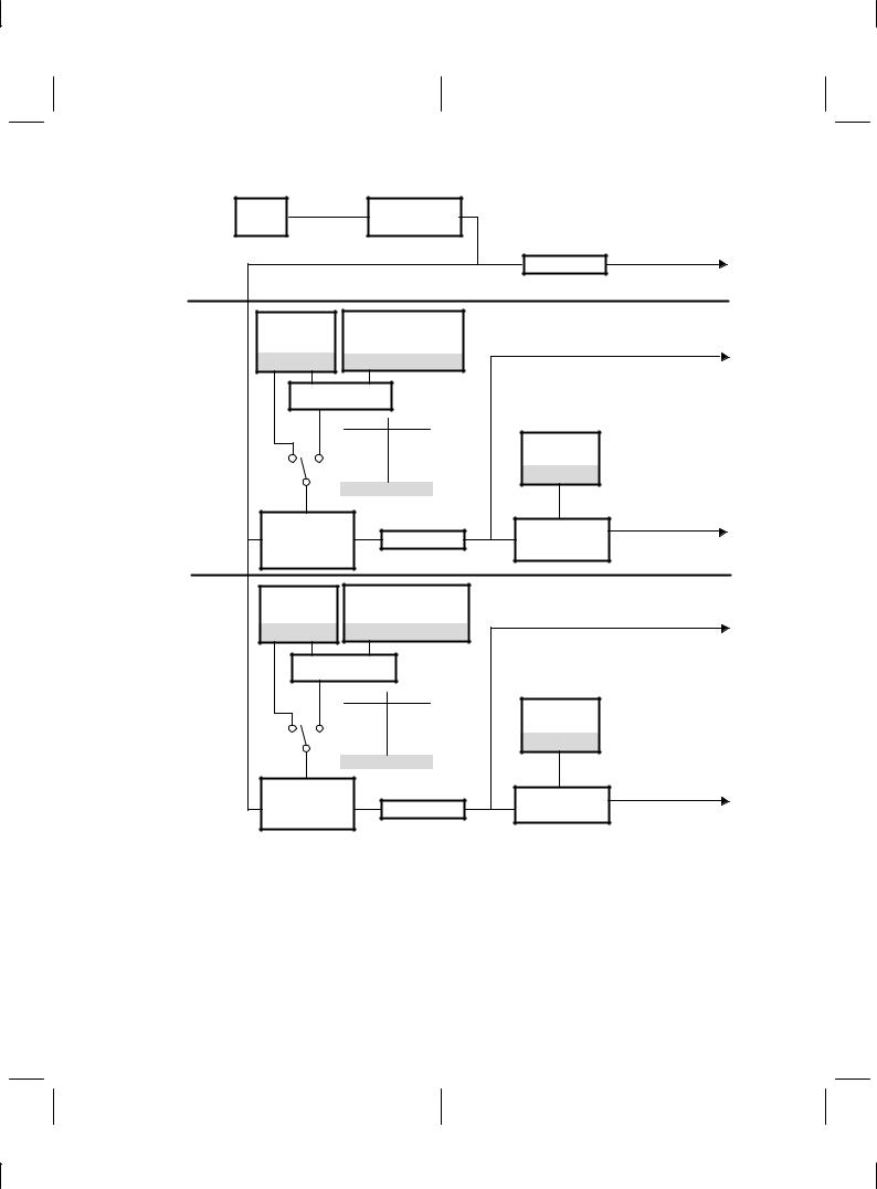
XTAL |
20.736 MHZ |
|
|
|
|
|
|
41.472 MHZ |
TMS320 DSP |
|
|
||||
OSC |
|
|
|
|
|||
|
|
|
|
|
|
|
|
|
MASTER CLOCK |
5.184 MHz |
|
SHIFT CLOCK |
|||
|
10.368 MHz |
Divide By 4 |
|||||
|
|
|
|
|
|
1.296 MHz |
|
|
|
|
|
|
|
|
|
|
|
|
|
|
|
|
2.592 MHz |
TA Register |
|
TA′REGISTER |
|
|
|||
|
|
(6 Bits) |
|
|
|||
(5 Bits) |
|
|
|
|
|||
2s-Complement TA |
|
SCF CLOCK |
|||||
See Table 2-3 |
|
||||||
|
See Table 2-3 |
|
Low-Pass Filter, |
||||
|
|
|
|
|
|
|
|
|
Adder/Subtractor |
|
|
(sin x)/x Filter |
|||
Transmit Section |
|
|
|
||||
|
|
|
|
|
|
|
|
D/A Conversion |
|
D1² D0 SELECT |
|
|
|||
Timing |
|
0 |
0 |
TA |
TB Register |
|
|
|
|
|
|||||
|
|
0 |
1 |
TA + TA′ |
7.20 kHz for TB = 40 |
||
|
|
(6 Bits) |
|||||
|
|
1 |
0 |
TA ± TA′ |
8.00 kHz for TB = 36 |
||
|
|
See Table 2-3 |
|||||
|
|
1 |
1 |
TA |
9.60 kHz for TB = 30 |
||
|
9 |
See Table 2-2 |
|
14.4 kHz for TB = 20 |
|||
|
18 |
|
|
|
|
|
16.0 kHz for TB = 18 |
|
|
|
|
|
|
19.2 kHz for TB = 15 |
|
|
|
|
|
|
|
|
|
TX (A) Counter |
|
Divide By 2 |
TX (B) Counter |
D/A Conversion |
|||
|
(6 Bits) |
|
576 kHz |
288 kHz |
|
||
|
|
|
Frequency |
||||
|
|
|
|
||||
RA Register |
|
RA′Register |
|
|
|||
|
(5 Bits) |
|
|
(6 Bits) |
|
|
|
See Table 2-3 |
2s-Complement RA |
|
SCF CLOCK |
||||
|
See Table 2-3 |
|
Low-Pass Filter |
||||
Receive Section |
|
|
|
|
|
|
|
|
|
|
|
|
|
|
|
A/D Conversion |
Adder/Subtractor |
|
|
|
|||
Timing |
|
|
|
|
|
|
|
|
|
D1² D0 SELECT |
RB Register |
|
|||
|
|
0 |
0 |
RA |
|
||
|
|
0 |
1 |
RA + RA′ |
(6 Bits) |
7.20 kHz for RB = 40 |
|
|
|
1 |
0 |
RA ± RA′ |
See Table 2-3 |
8.00 kHz for RB = 36 |
|
|
|
1 |
1 |
RA |
9.60 kHz for RB = 30 |
||
|
9 |
|
|||||
|
See Table 2-2 |
|
14.4 kHz for RB = 20 |
||||
|
18 |
|
|||||
|
|
|
|
|
|
16.0 kHz for RB = 18 |
|
|
|
|
|
|
|
|
|
|
|
|
|
|
|
|
19.2 kHz for RB = 15 |
RX (A) Counter |
|
Divide By 2 |
RX (B) Counter |
High-Pass Filter, |
|||
|
(6 Bits) |
|
|
|
|||
|
|
|
|
288 kHz |
|
||
|
|
|
576 kHz |
|
A/D Conversion |
||
|
|
|
|
|
|
|
Frequency |
² These control bits are described in the DX Serial Data Word Format section.
NOTES: A. Tables 2±2 and 2±3 are primary and secondary communication protocols, respectively.
B.In synchronous operation, RA, RA', RB, RX(A), and RX(B) are not used. TA, TA', TB, TX(A), and TX(B) are used instead.
C.Items in italics refer only to frequencies and register contents, which are variable. A crystal oscillator driving 20.736 MHz into the TMS320-series DSP provides a master clock frequency of 5.184 MHz. The TLC32046
produces a shift clock frequency of 1.296 MHz. If the TX(A) register contents equal 9, the SCF clock frequency is 288 kHz, and the D/A conversion frequency is 288 kHz ÷T(B).
Figure 2±1. Asynchronous Internal Timing Configuration
2±3

2.2Analog Input
Two pairs of analog inputs are provided. Normally, the IN+ and IN± input pair is used; however, the auxiliary input pair, AUX IN+ and AUX IN±, can be used if a second input is required. Since sufficient common-mode range and rejection are provided, each input set can be operated in differential or single-ended modes. The gain for the IN+, IN±, AUX IN+, and AUX IN± inputs can be programmed to 1, 2, or 4 (see Table 4±1). Either input circuit can be selected via software control. Multiplexing is controlled with the D4 bit (enable/disable AUX IN+ and AUX IN±) of the secondary DX word (see Table 2±3). The multiplexing requires a 2-ms wait at SCF = 288 kHz (see Figure 5±3) for a valid output signal. A wide dynamic range is ensured by the differential internal analog architecture and the separate analog and digital voltage supplies and grounds.
2.3A/D Band-Pass Filter, Clocking, and Conversion Timing
The receive-channel A/D high-pass filter can be selected or bypassed via software control (see Functional Block Diagram). The frequency response of this filter is found in the electrical characteristic section. This response results when the switched-capacitor filter clock frequency is 288 kHz and the A/D sample rate is 16 kHz. Several possible options can be used to attain a 288-kHz switched-capacitor filter clock. When the filter clock frequency is not 288 kHz, the low-pass filter transfer function is frequency-scaled by the ratio of the actual clock frequency to 288 kHz (see Typical Characteristics section). The ripple bandwidth and 3-dB low-frequency roll-off points of the high-pass section are 300 Hz and 200 Hz, respectively. However, the high-pass section low-frequency roll-off is frequency-scaled by the ratio of the A/D sample rate to 16 kHz.
Figure 2±1 and the DX serial data word format sections of this data manual indicate the many options for attaining a 288-kHz band-pass switched-capacitor filter clock. These sections indicate that the RX(A) counter can be programmed to give a 288-kHz band-pass switched-capacitor filter clock for several master clock input frequencies.
The A/D conversion rate is attained by frequency-dividing the band-pass switched-capacitor filter clock with the RX(B) counter. Unwanted aliasing is prevented because the A/D conversion rate is an integer submultiple of the band-pass switched-capacitor filter sampling rate, and the two rates are synchronously locked.
2.4A/D Converter
Fundamental performance specifications for the receive channel ADC circuitry are in the electrical characteristic section of this data manual. The ADC circuitry, using switched-capacitor techniques, provides an inherent sample-and-hold function.
2.5Analog Output
The analog output circuitry is an analog output power amplifier. Both noninverting and inverting amplifier outputs are brought out of the IC. This amplifier can drive transformer hybrids or low-impedance loads directly in either a differential or single-ended configuration.
2.6D/A Low-Pass Filter, Clocking, and Conversion Timing
The frequency response results when the low-pass switched-capacitor filter clock frequency is 288 kHz (see equation 1). Like the A/D filter, the transfer function of this filter is frequency-scaled when the clock frequency is not 288 kHz (see Typical Characteristics section). A continuous-time filter is provided on the output of the low-pass filter to eliminate the periodic sample data signal information, which occurs at multiples of the 288-kHz switched-capacitor clock feedthrough.
The D/A conversion rate is attained by frequency-dividing the 288-kHz switched-capacitor filter clock with the T(B) counter. Unwanted aliasing is prevented because the D/A conversion rate is an integer submultiple of the switched-capacitor low-pass filter sampling rate, and the two rates are synchronously locked.
2.7D/A Converter
Fundamental performance specifications for the transmit channel DAC circuitry are in the electrical characteristic section. The DAC has a sample-and-hold function that is realized with a switched-capacitor ladder.
2±4
 Loading...