


Texas Instruments TLC555CP, TLC555CDR, TLC555CD, TLC555QDR, TLC555MP Datasheet
...TLC555, TLC555Y
LinCMOS TIMERS
SLFS043C ± SEPTEMBER 1983 ± REVISED SEPTEMBER 1997
DVery Low Power Consumption
1mW Typ at VDD = 5 V
DCapable of Operation in Astable Mode
DCMOS Output Capable of Swinging Rail to Rail
DHigh Output-Current Capability
Sink 100 mA Typ
Source 10 mA Typ
D, DB, JG, P, OR PW PACKAGE
(TOP VIEW)
GND |
|
1 |
8 |
|
VDD |
|
|
||||
TRIG |
|
|
|
|
|
|
2 |
7 |
|
DISCH |
|
OUT |
|
3 |
6 |
|
THRES |
|
|
||||
RESET |
|
4 |
5 |
|
CONT |
|
|
||||
|
|
|
|
|
|
|
|
|
|
|
|
FK PACKAGE
D Output Fully Compatible With CMOS, TTL, |
|
(TOP VIEW) |
|
||||
and MOS |
|
NC |
GND |
NC |
DD |
|
|
|
|
|
|||||
D Low Supply Current Reduces Spikes |
|
V NC |
|
||||
|
|
|
|
|
|
||
During Output Transitions |
|
3 |
2 |
1 |
20 19 |
|
|
D Single-Supply Operation From 2 V to 15 V |
NC |
NC |
|||||
4 |
|
|
18 |
||||
D Functionally Interchangeable With the |
TRIG |
5 |
|
|
17 |
DISCH |
|
NC |
6 |
|
|
16 |
NC |
||
NE555; Has Same Pinout |
|
|
|||||
OUT |
7 |
|
|
15 |
THRES |
||
D ESD Protection Exceeds 2000 V Per |
|
|
|||||
NC |
8 |
|
|
14 |
NC |
||
MIL-STD-883C, Method 3015.2 |
|
|
|||||
|
9 |
10 11 12 13 |
|
||||
description |
|
NC |
RESET |
NC |
CONT NC |
|
|
The TLC555 is a monolithic timing circuit |
|
|
|||||
|
|
|
|
|
|
||
fabricated using the TI LinCMOS process. The |
NC ± No internal connection |
|
|||||
timer is fully compatible with CMOS, TTL, and |
|
|
|
|
|
|
|
MOS logic and operates at frequencies up to 2 MHz. Because of its high input impedance, this device uses |
|||||||
smaller timing capacitors than those used by the NE555. As a result, more accurate time delays and oscillations |
|||||||
are possible. Power consumption is low across the full range of power supply voltage. |
|
||||||
Like the NE555, the TLC555 has a trigger level equal to approximately one-third of the supply voltage and a threshold level equal to approximately two-thirds of the supply voltage. These levels can be altered by use of the control voltage terminal (CONT). When the trigger input (TRIG) falls below the trigger level, the flip-flop is set and the output goes high. If TRIG is above the trigger level and the threshold input (THRES) is above the threshold level, the flip-flop is reset and the output is low. The reset input (RESET) can override all other inputs and can be used to initiate a new timing cycle. If RESET is low, the flip-flop is reset and the output is low. Whenever the output is low, a low-impedance path is provided between the discharge terminal (DISCH) and GND. All unused inputs should be tied to an appropriate logic level to prevent false triggering.
While the CMOS output is capable of sinking over 100 mA and sourcing over 10 mA, the TLC555 exhibits greatly reduced supply-current spikes during output transitions. This minimizes the need for the large decoupling capacitors required by the NE555.
The TLC555C is characterized for operation from 0°C to 70°C. The TLC555I is characterized for operation from
± 40°C to 85°C. The TLC555M is characterized for operation over the full military temperature range of ± 55°C to 125°C.
This device contains circuits to protect its inputs and outputs against damage due to high static voltages or electrostatic fields. These circuits have been qualified to protect this device against electrostatic discharges (ESD) of up to 2 kV according to MIL-STD-883C, Method 3015; however, it is advised that precautions be taken to avoid application of any voltage higher than maximum-rated voltages to these high-impedance circuits. During storage or handling, the device leads should be shorted together or the device should be placed in conductive foam. In a circuit, unused inputs should always be connected to an appropriated logic voltage level, preferably either supply voltage or ground. Specific guidelines for handling devices of this type are contained in the publication
Guidelines for Handling Electrostatic-Discharge-Sensitive (ESDS) Devices and Assemblies available from Texas Instruments.
LinCMOS is a trademark of Texas Instruments Incorporated.
PRODUCTION DATA information is current as of publication date. Products conform to specifications per the terms of Texas Instruments standard warranty. Production processing does not necessarily include testing of all parameters.
Copyright 1997, Texas Instruments Incorporated
POST OFFICE BOX 655303 •DALLAS, TEXAS 75265 |
1 |
TLC555, TLC555Y |
|
|
|
|
|
|
|
|
||
LinCMOS |
TIMERS |
|
|
|
|
|
|
|
||
SLFS043C ± SEPTEMBER 1983 ± REVISED SEPTEMBER 1997 |
|
|
|
|
|
|
||||
|
|
|
|
|
|
|
|
|
|
|
|
|
|
|
AVAILABLE OPTIONS |
|
|
|
|
||
|
|
|
|
|
|
|
|
|
|
|
|
|
|
|
PACKAGED DEVICES |
|
|
|
CHIP |
|
|
|
|
|
|
|
|
|
|
|
|
|
|
|
|
SMALL |
|
CHIP |
CERAMIC |
PLASTIC |
|
|
|
|
|
VDD |
SSOP |
TSSOP |
FORM |
|
||||
TA |
|
OUTLINE |
CARRIER |
DIP |
DIP |
|
||||
|
RANGE |
(DB) |
(PW) |
(Y) |
|
|||||
|
|
|
(D) |
|
(FK) |
(JG) |
(P) |
|
|
|
0°C to |
2 V to 15 V |
TLC555CD |
TLC555CDBLE |
Ð |
Ð |
TLC555CP |
TLC555CPWLE |
|
|
|
70°C |
|
|
||||||||
|
|
|
|
|
|
|
|
|
|
|
|
|
|
|
|
|
|
|
|
|
|
± 40°C to |
3 V to 15 V |
TLC555ID |
Ð |
Ð |
Ð |
TLC555IP |
Ð |
TLC555Y |
|
|
85°C |
|
|||||||||
|
|
|
|
|
|
|
|
|
|
|
|
|
|
|
|
|
|
|
|
|
|
± 55°C to |
5 V to 15 V |
TLC555MD |
Ð |
TLC555MFK |
TLC555MJG |
TLC555MP |
Ð |
|
|
|
125°C |
|
|
||||||||
|
|
|
|
|
|
|
|
|
|
|
|
|
|
|
|
|
|
|
|
|
|
The D package is available taped and reeled. Add the R suffix to device type (e.g., TLC555CDR). The DB and PW packages are only available left-end taped and reeled (indicated by the LE suffix on the device type; e.g., TLC555CDBLE). Chips are tested at 25°C.
FUNCTION TABLE
RESET |
TRIGGER |
THRESHOLD |
OUTPUT |
DISCHARGE |
|
VOLTAGE² |
VOLTAGE² |
VOLTAGE² |
SWITCH |
||
|
|||||
<MIN |
Irrelevant |
Irrelevant |
L |
On |
|
|
|
|
|
|
|
>MAX |
<MIN |
Irrelevant |
H |
Off |
|
|
|
|
|
|
|
>MAX |
>MAX |
>MAX |
L |
On |
|
|
|
|
|
|
|
>MAX |
>MAX |
<MIN |
As previously established |
||
|
|
|
|
|
|
²For conditions shown as MIN or MAX, use the appropriate value specified under electrical characteristics.
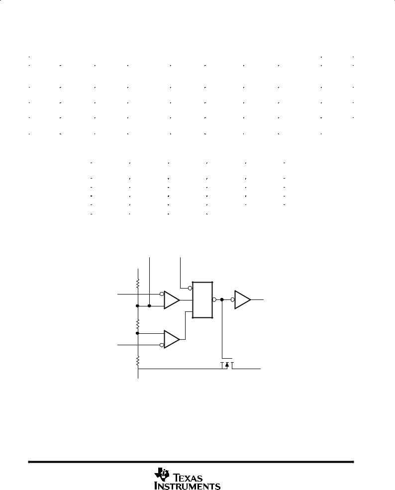
functional block diagram
CONT |
RESET |
|
5 |
4 |
|
VDD |
|
|
8 |
|
|
R |
R1 |
|
6 |
|
|
THRES |
|
3 |
|
R 1 |
OUT |
S
R
2
TRIG
R
7
 DISCH 1
GND
Pin numbers are for all packages except the FK package.
RESET can override TRIG, which can override THRES.
2 |
POST OFFICE BOX 655303 •DALLAS, TEXAS 75265 |
TLC555, TLC555Y
LinCMOS TIMERS
SLFS043C ± SEPTEMBER 1983 ± REVISED SEPTEMBER 1997
TLC555Y chip information
This chip, when properly assembled, displays characteristics similar to the TLC555. Thermal compression or ultrasonic bonding may be used on the doped aluminum bonding pads. Chips may be mounted with conductive epoxy or a gold-silicon preform.
BONDING PAD ASSIGNMENTS
50
64
CONT |
RESET |
|
(5) |
(4) |
|
VDD |
|
|
(8) |
|
|
R |
R1 |
|
(6) |
(3) |
|
THRES |
|
|
|
R 1 |
OUT |
S
R
(2)
TRIG
R
(7)
DISCH
(1) GND
RESET can override TRIG, which can override THRES.
CHIP THICKNESS: 15 TYPICAL
BONDING PADS: 4 × 4 MINIMUM
TJmax = 150°C
TOLERANCES ARE ± 10%.
ALL DIMENSIONS ARE IN MILS.
PIN (1) IS INTERNALLY CONNECTED
TO BACKSIDE OF CHIP.
POST OFFICE BOX 655303 •DALLAS, TEXAS 75265 |
3 |

4
75265 TEXAS DALLAS, •655303 BOX OFFICE POST
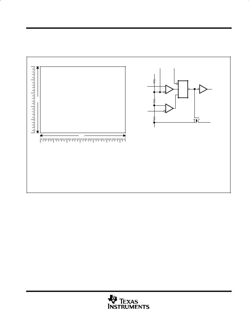
equivalent schematic (each channel) |
|
|
|
|
|
COMPONENT COUNT |
|
|
THRES |
Transistors |
39 |
|
Resistors |
5 |
|
|
|
||
|
|
|
VDD |
CONT |
|
|
|
|
|
|
OUT |
|
|
|
DISCH |
|
|
|
GND |
TRIG |
|
RESET |
|
1997 SEPTEMBER REVISED ± 1983 SEPTEMBER ± SLFS043C |
TLC555Y TLC555, TIMERS LinCMOS |
7±11±94 Date: Release Template |

TLC555, TLC555Y
LinCMOS TIMERS
SLFS043C ± SEPTEMBER 1983 ± REVISED SEPTEMBER 1997
absolute maximum ratings over operating free-air temperature range (unless otherwise noted)²
Supply voltage, VDD (see Note 1) . . . . . . . . . . . . . . . . . . . . . . . . . . . . . . . . . . . . . . . |
. . . . . . . . . . . |
. . . . . . . . . . 18 V |
Input voltage range, VI (any input) . . . . . . . . . . . . . . . . . . . . . . . . . . . . . . . . . . . . . . . |
. . . . . . . . . . . . |
. . ±0.3 to VDD |
Sink current, discharge or output . . . . . . . . . . . . . . . . . . . . . . . . . . . . . . . . . . . . . . . . |
. . . . . . . . . . . . |
. . . . . . 150 mA |
Source current, output, IO . . . . . . . . . . . . . . . . . . . . . . . . . . . . . . . . . . . . . . . . . . . . . . |
. . . . . . . . . . . . |
. . . . . . . 15 mA |
Continuous total power dissipation . . . . . . . . . . . . . . . . . . . . . . . . . . . . . . . . . . . . . |
See Dissipation Rating Table |
|
Operating free-air temperature range, TA: C-suffix . . . . . . . . . . . . . . . . . . . . . . . . |
. . . . . . . . . . . . |
. . 0°C to 70°C |
I-suffix . . . . . . . . . . . . . . . . . . . . . . . . |
. . . . . . . . . . . . |
±40°C to 85°C |
M-suffix . . . . . . . . . . . . . . . . . . . . . . . |
. . . . . . . . . . . |
±55°C to 125°C |
Storage temperature range . . . . . . . . . . . . . . . . . . . . . . . . . . . . . . . . . . . . . . . . . . . . . |
. . . . . . . . . . . |
±65°C to 150°C |
Case temperature for 60 seconds: FK package . . . . . . . . . . . . . . . . . . . . . . . . . . . |
. . . . . . . . . . . . |
. . . . . . . 260°C |
Lead temperature 1,6 mm (1/16 inch) from case for 60 seconds: JG package . |
. . . . . . . . . . . . |
. . . . . . . 300°C |
Lead temperature 1,6 mm (1/16 inch) from case for 10 seconds: D, DB, P, or PW package . |
. . . . . . . 260°C |
|
²Stresses beyond those listed under ªabsolute maximum ratingsº may cause permanent damage to the device. These are stress ratings only and functional operation of the device at these or any other conditions beyond those indicated under ªrecommended operating conditionsº is not
implied. Exposure to absolute-maximum-rated conditions for extended periods may affect device reliability. NOTE 1: All voltage values are with respect to network GND.
|
|
DISSIPATION RATING TABLE |
|
|
||
PACKAGE |
TA ≤ 25°C |
DERATING FACTOR |
TA = 70°C |
TA = 85°C |
TA = 125°C |
|
POWER RATING |
ABOVE TA = 25°C |
POWER RATING |
POWER RATING |
POWER RATING |
||
|
||||||
D |
725 mW |
5.8 mW/°C |
464 mW |
377 mW |
145 mW |
|
DB |
525 mW |
4.2 mW/°C |
336 mW |
273 mW |
105 mW |
|
FK |
1375 mW |
11.0 mW/°C |
880 mW |
715 mW |
275 mW |
|
JG |
1050 mW |
8.4 mW/°C |
672 mW |
546 mW |
210 mW |
|
P |
1000 mW |
8.0 mW/°C |
640 mW |
520 mW |
200 mW |
|
PW |
525 mW |
4.2 mW/°C |
336 mW |
273 mW |
105 mW |
|
|
|
|
|
|
|
|
recommended operating conditions
|
|
MIN |
MAX |
UNIT |
|
|
|
|
|
Supply voltage, VDD |
2 |
15 |
V |
|
|
TLC555C |
0 |
70 |
|
Operating free-air temperature range, TA |
|
|
|
°C |
TLC555I |
± 40 |
85 |
||
|
TLC555M |
± 55 |
125 |
|
|
|
|
|
|
POST OFFICE BOX 655303 •DALLAS, TEXAS 75265 |
5 |
TLC555, TLC555Y
LinCMOS TIMERS
SLFS043C ± SEPTEMBER 1983 ± REVISED SEPTEMBER 1997
electrical characteristics at specified free-air temperature, VDD = 2 V for TLC555C, VDD = 3 V for TLC555I
|
PARAMETER |
TEST |
T ² |
|
TLC555C |
|
|
TLC555I |
|
UNIT |
|
|
|
|
|
|
|
|
|||
|
|
CONDITIONS |
A |
MIN |
TYP |
MAX |
MIN |
TYP |
MAX |
|
|
|
|
|
|||||||
VIT |
Threshold voltage |
|
25°C |
0.95 |
1.33 |
1.65 |
1.6 |
|
2.4 |
V |
|
|
|
|
|
|
|
|
|||
|
Full range |
0.85 |
|
1.75 |
1.5 |
|
2.5 |
|||
|
|
|
|
|
|
|||||
|
|
|
|
|
|
|
|
|
|
|
IIT |
Threshold current |
|
25°C |
|
10 |
|
|
10 |
|
pA |
|
|
|
|
|
|
|
|
|||
|
MAX |
|
75 |
|
|
150 |
|
|||
|
|
|
|
|
|
|
|
|||
|
|
|
|
|
|
|
|
|
|
|
VI(TRIG) |
Trigger voltage |
|
25°C |
0.4 |
0.67 |
0.95 |
0.71 |
1 |
1.29 |
V |
|
|
|
|
|
|
|
|
|||
|
Full range |
0.3 |
|
1.05 |
0.61 |
|
1.39 |
|||
|
|
|
|
|
|
|||||
|
|
|
|
|
|
|
|
|
|
|
II(TRIG) |
Trigger current |
|
25°C |
|
10 |
|
|
10 |
|
pA |
|
|
|
|
|
|
|
|
|||
|
MAX |
|
75 |
|
|
150 |
|
|||
|
|
|
|
|
|
|
|
|||
|
|
|
|
|
|
|
|
|
|
|
VI(RESET) |
Reset voltage |
|
25°C |
0.4 |
1.1 |
1.5 |
0.4 |
1.1 |
1.5 |
V |
|
|
|
|
|
|
|
|
|||
|
Full range |
0.3 |
|
2 |
0.3 |
|
1.8 |
|||
|
|
|
|
|
|
|||||
|
|
|
|
|
|
|
|
|
|
|
II(RESET) |
Reset current |
|
25°C |
|
10 |
|
|
10 |
|
pA |
|
|
|
|
|
|
|
|
|||
|
MAX |
|
75 |
|
|
150 |
|
|||
|
|
|
|
|
|
|
|
|||
|
|
|
|
|
|
|
|
|
|
|
|
Control voltage (open circuit) as |
|
MAX |
|
66.7% |
|
|
66.7% |
|
|
|
a percentage of supply voltage |
|
|
|
|
|
|
|||
|
|
|
|
|
|
|
|
|
|
|
|
|
|
|
|
|
|
|
|
|
|
|
Discharge switch on-stage |
IOL = 1 mA |
25°C |
|
0.03 |
0.2 |
|
0.03 |
0.2 |
V |
|
voltage |
Full range |
|
|
0.25 |
|
|
0.375 |
||
|
|
|
|
|
|
|
||||
|
|
|
|
|
|
|
|
|
|
|
|
Discharge switch off-stage |
|
25°C |
|
0.1 |
|
|
0.1 |
|
nA |
|
current |
|
MAX |
|
0.5 |
|
|
120 |
|
|
|
|
|
|
|
|
|
||||
|
|
|
|
|
|
|
|
|
|
|
VOH |
High-level output voltage |
IOH = ±300 A |
25°C |
1.5 |
1.9 |
|
1.5 |
1.9 |
|
V |
|
|
|
|
|
|
|
||||
Full range |
1.5 |
|
|
2.5 |
|
|
||||
|
|
|
|
|
|
|
|
|||
|
|
|
|
|
|
|
|
|
|
|
VOL |
Low-level output voltage |
IOL = 1 mA |
25°C |
|
0.07 |
0.3 |
|
0.07 |
0.3 |
V |
|
|
|
|
|
|
|
||||
Full range |
|
|
0.35 |
|
|
0.4 |
||||
|
|
|
|
|
|
|
|
|||
|
|
|
|
|
|
|
|
|
|
|
IDD |
Supply current |
See Note 2 |
25°C |
|
|
250 |
|
|
250 |
A |
|
|
|
|
|
|
|
||||
Full range |
|
|
400 |
|
|
500 |
||||
|
|
|
|
|
|
|
|
|||
|
|
|
|
|
|
|
|
|
|
|
²Full range is 0°C to 70°C for the TLC555C and ± 40°C to 85°C for the TLC555I. For conditions shown as MAX, use the appropriate value specified in the recommended operating conditions table.
NOTE 2: These values apply for the expected operating configurations in which THRES is connected directly to DISCH or to TRIG.
6 |
POST OFFICE BOX 655303 •DALLAS, TEXAS 75265 |
 Loading...