


 Loading...
Texas Instruments TL081ACD, TL081ACP, TL081BCD, TL081BCP, TL081CD Schematic [ru]
...PRODUCT |
SAMPLE & |
TECHNICAL |
TOOLS & |
SUPPORT & |
FOLDER |
BUY |
DOCUMENTS |
SOFTWARE |
COMMUNITY |
TL081, TL081A, TL081B, TL082, TL082A
TL082B, TL084, TL084A, TL084B
SLOS081I –FEBRUARY 1977 –REVISED MAY 2015
TL08xx JFET-Input Operational Amplifiers
1 Features
•Low Power Consumption: 1.4 mA/ch Typical
•Wide Common-Mode and Differential Voltage Ranges
•Low Input Bias Current: 30 pA Typical
•Low Input Offset Current: 5 pA Typical
•Output Short-Circuit Protection
•Low Total Harmonic Distortion: 0.003% Typical
•High Input Impedance: JFET Input Stage
•Latch-Up-Free Operation
•High Slew Rate: 13 V/μs Typical
•Common-Mode Input Voltage Range Includes VCC+
2 Applications
•Tablets
•White goods
•Personal electronics
3 Description
The TL08xx JFET-input operational amplifier family is designed to offer a wider selection than any previously developed operational amplifier family. Each of these JFET-input operational amplifiers incorporates well-matched, high-voltage JFET and bipolar transistors in a monolithic integrated circuit. The devices feature high slew rates, low input bias and offset currents, and low offset-voltage temperature coefficient.
Device Information(1)
PART NUMBER |
PACKAGE |
BODY SIZE (NOM) |
TL084xD |
SOIC (14) |
8.65 mm × 3.91 mm |
TL08xxFK |
LCCC (20) |
8.89 mm × 8.89 mm |
TL084xJ |
CDIP (14) |
19.56 mm × 6.92 mm |
TL084xN |
PDIP (14) |
19.3 mm × 6.35 mm |
TL084xNS |
SO (14) |
10.3 mm × 5.3 mm |
TL084xPW |
TSSOP (14) |
5.0 mm × 4.4 mm |
(1)For all available packages, see the orderable addendum at the end of the data sheet.
•Computers
Schematic Symbol
|
TL081 |
|
TL082 (EACH AMPLIFIER) |
||||||||
|
|
|
|
|
|
|
TL084 (EACH AMPLIFIER) |
||||
OFFSET N1 |
|
|
|
|
|
|
|
|
|
|
|
|
+ |
|
|
|
|
|
|
|
|
|
|
IN + |
|
|
|
OUT |
IN + |
|
|
+ |
|
OUT |
|
|
|
|
|
|
|
||||||
|
|
|
|
|
|
||||||
|
|
|
|
|
|||||||
|
|
− |
|
|
|
|
|
|
|
||
|
|
|
|
|
|
|
|
|
|||
IN − |
|
|
|
|
IN − |
|
|
− |
|||
|
|||||||||||
|
|
|
|
|
|
||||||
OFFSET N2 |
|
|
|
|
|
|
|
|
|
|
|
|
|
|
|
|
|
|
|
|
|
|
|
|
|
|
|
|
|
|
|
|
|
|
|
An IMPORTANT NOTICE at the end of this data sheet addresses availability, warranty, changes, use in safety-critical applications, intellectual property matters and other important disclaimers. PRODUCTION DATA.

TL081, TL081A, TL081B, TL082, TL082A
TL082B, TL084, TL084A, TL084B
SLOS081I –FEBRUARY 1977 –REVISED MAY 2015 |
www.ti.com |
Table of Contents
1 |
Features .................................................................. |
1 |
|
2 |
Applications ........................................................... |
1 |
|
3 |
Description ............................................................. |
1 |
|
4 |
Revision History..................................................... |
2 |
|
5 |
Pin Configuration and Functions ......................... |
3 |
|
6 |
Specifications......................................................... |
5 |
|
|
6.1 |
Absolute Maximum Ratings ..................................... |
5 |
|
6.2 |
ESD Ratings.............................................................. |
5 |
|
6.3 |
Recommended Operating Conditions....................... |
5 |
|
6.4 |
Thermal Information .................................................. |
6 |
|
6.5 |
Electrical Characteristics for TL08xC, TL08xxC, and |
|
|
|
TL08xI ........................................................................ |
6 |
|
6.6 |
Electrical Characteristics for TL08xM and TL084x ... |
7 |
|
6.7 |
Operating Characteristics.......................................... |
7 |
|
6.8 |
Dissipation Rating Table ........................................... |
8 |
|
6.9 |
Typical Characteristics .............................................. |
9 |
7 |
Parameter Measurement Information ................ |
13 |
|
8 |
Detailed Description ............................................ |
14 |
|
|
8.1 |
Overview ................................................................. |
14 |
|
8.2 |
Functional Block Diagram ....................................... |
14 |
|
8.3 |
Feature Description................................................. |
14 |
|
8.4 |
Device Functional Modes........................................ |
14 |
9 |
Applications and Implementation ...................... |
15 |
|
|
9.1 |
Application Information............................................ |
15 |
|
9.2 |
Typical Applications ............................................... |
15 |
|
9.3 |
System Examples ................................................... |
16 |
10 |
Power Supply Recommendations ..................... |
18 |
|
11 |
Layout................................................................... |
18 |
|
|
11.1 |
Layout Guidelines ................................................. |
18 |
|
11.2 |
Layout Examples................................................... |
19 |
12 Device and Documentation Support ................. |
20 |
||
|
12.1 |
Documentation Support ........................................ |
20 |
|
12.2 |
Related Links ........................................................ |
20 |
|
12.3 |
Community Resources.......................................... |
20 |
|
12.4 |
Trademarks ........................................................... |
20 |
|
12.5 |
Electrostatic Discharge Caution............................ |
20 |
|
12.6 |
Glossary ................................................................ |
20 |
13 Mechanical, Packaging, and Orderable |
|
||
|
Information ........................................................... |
20 |
|
4 Revision History
NOTE: Page numbers for previous revisions may differ from page numbers in the current version.
Changes from Revision H (January 2014) to Revision I |
Page |
•Added Pin Configuration and Functions section, Storage Conditions table, ESD Ratings table, Feature Description section, Device Functional Modes, Application and Implementation section, Power Supply Recommendations section, Layout section, Device and Documentation Support section, and Mechanical, Packaging, and Orderable
Information section ................................................................................................................................................................ |
1 |
• Added Applications................................................................................................................................................................. |
1 |
• Moved Typical Characteristics into Specifications section. ................................................................................................... |
9 |
Changes from Revision G (September 2004) to Revision H |
Page |
• Updated document to new TI data sheet format - no specification changes. ........................................................................ |
1 |
• Deleted Ordering Information table. ....................................................................................................................................... |
1 |
2 |
Submit Documentation Feedback |
Copyright © 1977–2015, Texas Instruments Incorporated |
|
Product Folder Links: TL081 TL081A TL081B TL082 TL082A TL082B TL084 TL084A TL084B |
|
TL081, TL081A, TL081B, TL082, TL082A
TL082B, TL084, TL084A, TL084B
www.ti.com |
SLOS081I –FEBRUARY 1977–REVISED MAY 2015 |
5 Pin Configuration and Functions
|
TL082 FK Package |
|
TL081 and TL081x D, P, and PS Package |
|||||||
|
20-Pin LCCC |
|
||||||||
|
|
Top View |
|
|
8-Pin SOIC, PDIP, and SO |
|||||
|
|
|
|
|
Top View |
|
||||
|
NC 1OUT |
|
CC+ |
|
|
|
|
|||
|
NC |
NC |
|
OFFSET N1 |
1 |
8 |
NC |
|||
|
V |
|
||||||||
|
|
|
|
|
|
|
IN − |
2 |
7 |
VCC + |
NC |
3 |
2 |
1 |
20 19 |
NC |
IN + |
3 |
6 |
OUT |
|
4 |
|
|
|
18 |
||||||
|
|
|
|
|
|
|
||||
1IN − |
5 |
|
|
|
17 |
2OUT |
VCC − |
4 |
5 |
OFFSET N2 |
NC |
6 |
|
|
|
16 |
NC |
|
|
|
|
1IN + |
7 |
|
|
|
15 |
2IN − |
TL082 and TL082x D, JG, P, PS and PW Package |
|||
NC |
8 |
|
|
|
14 |
NC |
||||
|
9 10 11 12 13 |
|
8-Pin SOIC, CDIP, PDIP, SO, and TSSOP |
|||||||
|
NC |
|
NC |
2IN+ |
NC |
|
|
Top View |
|
|
|
V |
|
|
|
|
|
||||
|
|
− |
|
|
|
|
|
|
|
|
|
|
CC |
|
|
|
|
1OUT |
1 |
8 |
VCC + |
|
|
|
|
|
|
|
||||
|
|
|
|
|
|
|
1IN − |
2 |
7 |
2OUT |
|
|
|
|
|
|
|
1IN + |
3 |
6 |
2IN − |
|
TL084 FK Package |
|
VCC − |
4 |
5 |
2IN + |
||||
|
20-Pin LCCC |
|
|
|
|
|
||||
|
1IN− |
Top View |
4IN− |
|
|
|
|
|
||
|
1OUT |
NC |
4OUT |
|
TL084 and TL084x D, J, N, NS and PW Package |
|||||
|
|
|
|
|
|
|
14-Pin SOIC, CDIP, PDIP, SO, and TSSOP |
|||
|
|
|
|
|
|
|
|
Top View |
|
|
1IN + |
3 |
2 |
1 |
20 19 |
4IN + |
|
|
|
|
|
4 |
|
|
|
18 |
1OUT |
1 |
14 |
4OUT |
||
|
|
|
|
|
|
|
||||
NC |
5 |
|
|
|
17 |
NC |
1IN − |
2 |
13 |
4IN − |
|
|
|
|
|
|
|
||||
VCC + |
6 |
|
|
|
16 |
VCC − |
1IN + |
3 |
12 |
4IN + |
NC |
7 |
|
|
|
15 |
NC |
VCC + |
4 |
11 |
VCC − |
|
|
|
|
|
|
|
||||
2IN + |
8 |
|
|
|
14 |
3IN + |
2IN + |
5 |
10 |
3IN + |
|
9 10 11 12 13 |
|
||||||||
|
|
2IN − |
|
|
3IN − |
|||||
|
2IN− |
2OUT |
NC |
3OUT |
3IN− |
|
6 |
9 |
||
|
|
2OUT |
7 |
8 |
3OUT |
|||||
Pin Functions
|
|
|
PIN |
|
|
|
|
|
|
|
|
|
|
TL081 |
TL082 |
|
TL084 |
|
|
|
|
||
NAME |
|
|
SOIC, |
|
|
SOIC, |
|
|
I/O |
DESCRIPTION |
|
|
SOIC, PDIP, |
|
LCCC |
CDIP, |
|
LCCC |
|
|
|
||
|
|
CDIP, PDIP, |
|
|
|
|
|
||||
|
|
SO |
SO, TSSOP |
|
|
PDIP, SO, |
|
|
|
|
|
|
|
|
|
|
TSSOP |
|
|
|
|
|
|
|
|
|
|
|
|
|
|
|
|
|
|
1IN– |
— |
2 |
|
5 |
2 |
|
3 |
I |
Negative input |
|
|
1IN+ |
— |
3 |
|
7 |
3 |
|
4 |
I |
Positive input |
|
|
1OUT |
— |
1 |
|
2 |
1 |
|
2 |
O |
Output |
|
|
2IN– |
— |
6 |
|
15 |
6 |
|
9 |
I |
Negative input |
|
|
2IN+ |
— |
5 |
|
12 |
5 |
|
8 |
I |
Positive input |
|
|
2OUT |
— |
7 |
|
17 |
7 |
|
10 |
O |
Output |
|
|
3IN– |
— |
— |
|
— |
9 |
|
13 |
I |
Negative input |
|
|
3IN+ |
— |
— |
|
— |
10 |
|
14 |
I |
Positive input |
|
|
3OUT |
— |
— |
|
— |
8 |
|
12 |
O |
Output |
|
|
4IN– |
— |
— |
|
— |
13 |
|
19 |
I |
Negative input |
|
|
4IN+ |
— |
— |
|
— |
12 |
|
18 |
I |
Positive input |
|
|
4OUT |
— |
— |
|
— |
14 |
|
20 |
O |
Output |
|
|
|
|
|
|
|
|
|
|
|
|
|
|
Copyright © 1977–2015, Texas Instruments Incorporated |
|
|
|
|
Submit Documentation Feedback |
3 |
|||||
Product Folder Links: TL081 TL081A TL081B TL082 TL082A TL082B TL084 TL084A TL084B

TL081, TL081A, TL081B, TL082, TL082A
TL082B, TL084, TL084A, TL084B
SLOS081I –FEBRUARY 1977 –REVISED MAY 2015 www.ti.com
Pin Functions (continued)
|
|
|
PIN |
|
|
|
|
|
|
|
|
|
TL081 |
TL082 |
|
TL084 |
|
|
|
||
NAME |
|
|
SOIC, |
|
|
SOIC, |
|
|
I/O |
DESCRIPTION |
|
SOIC, PDIP, |
|
LCCC |
CDIP, |
|
LCCC |
|
|
||
|
|
CDIP, PDIP, |
|
|
|
|
||||
|
|
SO |
SO, TSSOP |
|
|
PDIP, SO, |
|
|
|
|
|
|
|
|
|
TSSOP |
|
|
|
|
|
|
|
|
|
|
|
|
|
|
|
|
IN– |
2 |
— |
|
— |
— |
|
— |
I |
Negative input |
|
IN+ |
3 |
— |
|
— |
— |
|
— |
I |
Positive input |
|
|
|
|
|
|
1 |
|
|
1 |
|
|
|
|
|
|
|
3 |
|
|
|
|
|
|
|
|
|
|
|
|
|
|
|
|
|
|
|
|
|
4 |
|
|
5 |
|
|
|
|
|
|
|
6 |
|
|
|
|
|
|
|
|
|
|
|
|
|
|
|
|
|
|
|
|
|
8 |
|
|
7 |
|
|
NC |
8 |
— |
|
9 |
— |
|
— |
Do not connect |
||
|
|
|
||||||||
|
|
|
|
|
11 |
|
|
11 |
|
|
|
|
|
|
|
13 |
|
|
|
|
|
|
|
|
|
|
|
|
|
|
|
|
|
|
|
|
|
14 |
|
|
15 |
|
|
|
|
|
|
|
16 |
|
|
|
|
|
|
|
|
|
|
|
|
|
|
|
|
|
|
|
|
|
18 |
|
|
17 |
|
|
OFFSET |
1 |
— |
|
— |
— |
|
— |
— |
Input offset adjustment |
|
N1 |
|
|
||||||||
|
|
|
|
|
|
|
|
|
||
OFFSET |
5 |
— |
|
— |
— |
|
— |
— |
Input offset adjustment |
|
N2 |
|
|
||||||||
|
|
|
|
|
|
|
|
|
||
OUT |
6 |
— |
|
— |
— |
|
— |
O |
Output |
|
VCC– |
4 |
4 |
|
10 |
11 |
|
16 |
— |
Power supply |
|
VCC+ |
7 |
8 |
|
20 |
4 |
|
6 |
— |
Power supply |
|
4 |
Submit Documentation Feedback |
Copyright © 1977–2015, Texas Instruments Incorporated |
|
Product Folder Links: TL081 TL081A TL081B TL082 TL082A TL082B TL084 TL084A TL084B |
|

TL081, TL081A, TL081B, TL082, TL082A
TL082B, TL084, TL084A, TL084B
www.ti.com |
SLOS081I –FEBRUARY 1977–REVISED MAY 2015 |
6 Specifications
6.1 Absolute Maximum Ratings
over operating free-air temperature range (unless otherwise noted)(1)
|
|
|
|
MIN |
MAX |
UNIT |
VCC+ |
Supply voltage(2) |
|
|
|
18 |
V |
VCC– |
|
|
|
–18 |
||
|
|
|
|
|
||
VID |
Differential input voltage(3) |
|
|
|
±30 |
V |
VI |
Input voltage(2)(4) |
|
|
|
±15 |
V |
|
Duration of output short circuit(5) |
|
|
|
Unlimited |
|
|
Continuous total power dissipation |
|
|
See Dissipation Rating Table |
|
|
|
|
|
TL08_C |
|
|
|
|
|
|
TL08_AC |
0 |
70 |
|
|
|
|
TL08_BC |
|
|
|
TA |
Operating free-air temperature |
|
TL08_I |
–40 |
85 |
°C |
|
|
|
TL084Q |
–40 |
125 |
|
|
|
|
TL08_M |
–55 |
125 |
|
|
|
|
|
|
|
|
|
Operating virtual junction temperature |
|
|
150 |
°C |
|
|
|
|
|
|
|
|
TC |
Case temperature for 60 seconds |
FK package |
TL08_M |
|
260 |
°C |
|
Lead temperature 1,6 mm (1/16 |
J or JG package |
TL08_M |
|
300 |
°C |
|
inch) from case for 10 seconds |
|
||||
|
|
|
|
|
|
|
Tstg |
Storage temperature |
|
|
–65 |
150 |
°C |
(1)Stresses beyond those listed under Absolute Maximum Ratings may cause permanent damage to the device. These are stress ratings only, and functional operation of the device at these or any other conditions beyond those indicated under Recommended Operating Conditions is not implied. Exposure to absolute-maximum-rated conditions for extended periods may affect device reliability.
(2)All voltage values, except differential voltages, are with respect to the midpoint between VCC+ and VCC−.
(3)Differential voltages are at IN+, with respect to IN−.
(4)The magnitude of the input voltage must never exceed the magnitude of the supply voltage or 15 V, whichever is less.
(5)The output may be shorted to ground or to either supply. Temperature and/or supply voltages must be limited to ensure that the dissipation rating is not exceeded.
6.2 |
ESD Ratings |
|
|
|
|
|
|
VALUE |
UNIT |
|
|
Human body model (HBM), per ANSI/ESDA/JEDEC JS-001(1) |
1000 |
|
V(ESD) |
Electrostatic discharge |
Charged-device model (CDM), per JEDEC specification JESD22- |
1500 |
V |
|
|
C101(2) |
|
(1)JEDEC document JEP155 states that 500-V HBM allows safe manufacturing with a standard ESD control process.
(2)JEDEC document JEP157 states that 250-V CDM allows safe manufacturing with a standard ESD control process.
6.3 Recommended Operating Conditions
over operating free-air temperature range (unless otherwise noted)
|
|
|
MIN |
MAX |
UNIT |
|
VCC+ |
Supply voltage |
5 |
15 |
V |
||
VCC– |
Supply voltage |
–5 |
–15 |
V |
||
VCM |
Common-mode voltage |
VCC– + 4 |
VCC+ – 4 |
V |
||
|
|
TL08xM |
–55 |
125 |
|
|
TA |
Ambient temperature |
TL08xQ |
–40 |
125 |
°C |
|
TL08xI |
–40 |
85 |
||||
|
|
|
||||
|
|
TL08xC |
0 |
70 |
|
|
Copyright © 1977–2015, Texas Instruments Incorporated |
Submit Documentation Feedback |
5 |
Product Folder Links: TL081 TL081A TL081B TL082 TL082A TL082B TL084 TL084A TL084B |
|
|

TL081, TL081A, TL081B, TL082, TL082A
TL082B, TL084, TL084A, TL084B
SLOS081I –FEBRUARY 1977 –REVISED MAY 2015 www.ti.com
6.4 |
Thermal Information |
|
|
|
|
|
|
|
|
|
|
|
|
|
|
|
TL08xx |
|
|
|
|
|
|
|
THERMAL METRIC(1) |
D (SOIC) |
N (PDIP) |
NS (SO) |
|
P (PDIP) |
PS (SO) |
PW (TSSOP) |
UNIT |
||
|
8 PINS |
14 |
14 PINS |
14 PINS |
|
{PIN |
{PIN |
8 PINS |
14 |
||
|
|
|
|
||||||||
|
|
|
PINS |
|
|
|
COUNT} |
COUNT} |
|
PINS |
|
|
|
|
|
|
|
|
PINS |
PINS |
|
|
|
RθJA |
Junction-to-ambient |
97 |
86 |
76 |
80 |
|
85 |
95 |
149 |
113 |
°C/W |
thermal resistance(2)(3) |
|
||||||||||
(1)For more information about traditional and new thermal metrics, see the Semiconductor and IC Package Thermal Metrics application report, SPRA953.
(2)Maximum power dissipation is a function of TJ(max), RθJA, and TA. The maximum allowable power dissipation at any allowable ambient temperature is PD = (TJ(max) – TA) / RθJA. Operating at the absolute maximum TJ of 150°C can affect reliability.
(3)The package thermal impedance is calculated in accordance with JESD 51-7.
6.5 Electrical Characteristics for TL08xC, TL08xxC, and TL08xI
VCC± = ±15 V (unless otherwise noted)
|
|
|
TEST |
|
TL081C, TL082C, |
TL081AC, TL082AC, |
TL081BC, TL082BC, |
TL081I, TL082I, |
|
|||||||||||
|
PARAMETER |
TA(1) |
|
TL084C |
|
|
TL084AC |
|
|
TL084BC |
|
|
TL084I |
|
UNIT |
|||||
|
|
|
CONDITIONS |
|
|
|
|
|
|
|
|
|
|
|
|
|
|
|
|
|
|
|
|
|
MIN |
TYP |
MAX |
MIN |
TYP |
MAX |
MIN |
|
TYP |
MAX |
MIN |
TYP |
MAX |
|
|||
|
|
|
|
|
|
|
||||||||||||||
|
|
Input offset |
VO = 0, |
25°C |
|
3 |
15 |
|
3 |
|
6 |
|
2 |
|
3 |
|
3 |
6 |
|
|
VIO |
|
Full |
|
|
|
|
|
|
|
|
|
|
|
|
|
|
|
mV |
||
|
voltage |
RS = 50 Ω |
|
|
20 |
|
|
|
7.5 |
|
|
|
|
5 |
|
|
9 |
|||
|
|
|
|
range |
|
|
|
|
|
|
|
|
|
|
|
|
|
|
|
|
|
|
Temperature |
|
|
|
|
|
|
|
|
|
|
|
|
|
|
|
|
|
|
αVIO |
|
coefficient of |
VO = 0, |
Full |
|
18 |
|
|
18 |
|
|
|
18 |
|
|
|
18 |
|
μV/°C |
|
|
input |
RS = 50 Ω |
range |
|
|
|
|
|
|
|
|
|
|
|||||||
|
|
offset |
|
|
|
|
|
|
|
|
|
|
|
|
|
|
|
|
||
|
|
voltage |
|
|
|
|
|
|
|
|
|
|
|
|
|
|
|
|
|
|
|
|
|
|
|
|
|
|
|
|
|
|
|
|
|
|
|
|
|
|
|
|
|
Input offset |
|
25°C |
|
5 |
200 |
|
5 |
|
100 |
|
5 |
|
100 |
|
5 |
100 |
pA |
|
IIO |
|
VO = 0 |
Full |
|
|
|
|
|
|
|
|
|
|
|
|
|
|
|
|
|
|
current(2) |
|
|
2 |
|
|
|
2 |
|
|
|
|
2 |
|
|
10 |
nA |
|||
|
|
|
|
range |
|
|
|
|
|
|
|
|
|
|
|
|
|
|
|
|
|
|
Input bias |
|
25°C |
|
30 |
400 |
|
30 |
|
200 |
|
30 |
|
200 |
|
30 |
200 |
pA |
|
IIB |
|
VO = 0 |
Full |
|
|
|
|
|
|
|
|
|
|
|
|
|
|
|
|
|
|
current(2) |
|
|
10 |
|
|
|
7 |
|
|
|
|
7 |
|
|
20 |
nA |
|||
|
|
|
|
range |
|
|
|
|
|
|
|
|
|
|
|
|
|
|
|
|
|
|
Common- |
|
|
|
–12 |
|
|
–12 |
|
|
|
–12 |
|
|
–12 |
|
|
||
|
|
mode |
|
|
|
|
|
|
|
|
|
|
|
|
||||||
VICR |
|
|
25°C |
±11 |
to |
|
±11 |
to |
|
±11 |
|
to |
|
±11 |
to |
|
V |
|||
|
input voltage |
|
|
|
|
|
|
|||||||||||||
|
|
|
|
|
15 |
|
|
15 |
|
|
|
15 |
|
|
|
15 |
|
|
||
|
|
range |
|
|
|
|
|
|
|
|
|
|
|
|
|
|||||
|
|
|
|
|
|
|
|
|
|
|
|
|
|
|
|
|
|
|
|
|
|
|
|
|
|
|
|
|
|
|
|
|
|
|
|
|
|
|
|
|
|
|
|
Maximum |
RL = 10 kΩ |
25°C |
±12 |
±13.5 |
|
±12 |
±13.5 |
|
|
±12 |
±13.5 |
|
|
±12 |
±13.5 |
|
|
|
|
|
peak |
|
|
|
|
|
|
|
|
|
|
|
|
|
|
|
|
|
|
|
|
RL ≥ 10 kΩ |
|
±12 |
|
|
±12 |
|
|
|
±12 |
|
|
|
|
±12 |
|
|
|
|
VOM |
|
output |
Full |
|
|
|
|
|
|
|
|
|
|
|
V |
|||||
|
|
|
|
|
|
|
|
|
|
|
|
|
|
|
|
|
||||
|
|
voltage |
RL ≥ 2 kΩ |
range |
±10 |
±12 |
|
±10 |
±12 |
|
|
±10 |
±12 |
|
|
±10 |
±12 |
|
|
|
|
|
swing |
|
|
|
|
|
|
|
|||||||||||
|
|
|
|
|
|
|
|
|
|
|
|
|
|
|
|
|
|
|
|
|
|
|
Large-signal |
|
25°C |
25 |
200 |
|
50 |
200 |
|
|
50 |
200 |
|
|
50 |
200 |
|
|
|
AVD |
|
differential |
VO = ±10 V, |
|
|
|
|
|
|
|
|
|
|
|
|
|
|
|
|
V/mV |
|
Full |
|
|
|
|
|
|
|
|
|
|
|
|
|
|
|
||||
|
voltage |
RL ≥ 2 kΩ |
15 |
|
|
15 |
|
|
|
25 |
|
|
|
|
25 |
|
|
|||
|
|
amplification |
|
range |
|
|
|
|
|
|
|
|
|
|
|
|
|
|
|
|
B1 |
|
Unity-gain |
|
25°C |
|
3 |
|
|
3 |
|
|
|
3 |
|
|
|
3 |
|
MHz |
|
|
bandwidth |
|
|
|
|
|
|
|
|
|
|
|
||||||||
|
|
|
|
|
|
|
|
|
|
|
|
|
|
|
|
|
|
|
|
|
ri |
|
Input |
|
25°C |
|
1012 |
|
|
1012 |
|
|
|
1012 |
|
|
|
1012 |
|
Ω |
|
|
resistance |
|
|
|
|
|
|
|
|
|
|
|
||||||||
|
|
|
|
|
|
|
|
|
|
|
|
|
|
|
|
|
|
|
|
|
|
|
Common- |
VIC = VICRmin, |
|
|
|
|
|
|
|
|
|
|
|
|
|
|
|
|
|
|
|
mode |
|
|
|
|
|
|
|
|
|
|
|
|
|
|
|
|
|
|
CMRR |
VO = 0, |
25°C |
70 |
86 |
|
75 |
86 |
|
|
75 |
86 |
|
|
75 |
86 |
|
dB |
|||
rejection |
|
|
|
|
|
|
||||||||||||||
|
|
RS = 50 Ω |
|
|
|
|
|
|
|
|
|
|
|
|
|
|
|
|
|
|
|
|
ratio |
|
|
|
|
|
|
|
|
|
|
|
|
|
|
|
|
|
|
|
|
|
|
|
|
|
|
|
|
|
|
|
|
|
|
|
|
|
|
|
|
|
|
|
|
|
|
|
|
|
|
|
|
|
|
|
|
|
|
|
|
|
|
Supply- |
VCC = ±15 V to |
|
|
|
|
|
|
|
|
|
|
|
|
|
|
|
|
|
|
|
voltage |
|
|
|
|
|
|
|
|
|
|
|
|
|
|
|
|
|
|
|
|
±9 V, |
|
|
|
|
|
|
|
|
|
|
|
|
|
|
|
|
|
|
kSVR |
|
rejection |
25°C |
70 |
86 |
|
80 |
86 |
|
|
80 |
86 |
|
|
80 |
86 |
|
dB |
||
|
VO = 0, |
|
|
|
|
|
|
|||||||||||||
|
|
ratio |
|
|
|
|
|
|
|
|
|
|
|
|
|
|
|
|
|
|
|
|
RS = 50 Ω |
|
|
|
|
|
|
|
|
|
|
|
|
|
|
|
|
|
|
|
|
( VCC±/ VIO) |
|
|
|
|
|
|
|
|
|
|
|
|
|
|
|
|
|
|
(1)All characteristics are measured under open-loop conditions with zero common-mode voltage, unless otherwise specified. Full range for TA is 0°C to 70°C for TL08_C, TL08_AC, TL08_BC and –40°C to 85°C for TL08_I.
(2)Input bias currents of an FET-input operational amplifier are normal junction reverse currents, which are temperature sensitive, as shown in Figure 13. Pulse techniques must be used that maintain the junction temperature as close to the ambient temperature as possible.
6 |
Submit Documentation Feedback |
Copyright © 1977–2015, Texas Instruments Incorporated |
|
Product Folder Links: TL081 TL081A TL081B TL082 TL082A TL082B TL084 TL084A TL084B |
|
TL081, TL081A, TL081B, TL082, TL082A
TL082B, TL084, TL084A, TL084B
www.ti.com |
SLOS081I –FEBRUARY 1977–REVISED MAY 2015 |
Electrical Characteristics for TL08xC, TL08xxC, and TL08xI (continued)
VCC± = ±15 V (unless otherwise noted)
|
|
TEST |
|
TL081C, TL082C, |
TL081AC, TL082AC, |
TL081BC, TL082BC, |
TL081I, TL082I, |
|
||||||||
|
PARAMETER |
TA(1) |
|
TL084C |
|
TL084AC |
|
TL084BC |
|
|
TL084I |
|
UNIT |
|||
|
|
CONDITIONS |
|
MIN |
TYP |
MAX |
MIN TYP |
MAX |
MIN TYP |
MAX |
MIN TYP |
MAX |
|
|||
|
|
|
|
|
||||||||||||
|
Supply |
|
|
|
|
|
|
|
|
|
|
|
|
|
|
|
ICC |
current |
VO = 0, |
25°C |
|
1.4 |
2.8 |
1.4 |
|
2.8 |
1.4 |
|
2.8 |
1.4 |
2.8 |
mA |
|
(each |
No load |
|
|
|
||||||||||||
|
amplifier) |
|
|
|
|
|
|
|
|
|
|
|
|
|
|
|
|
|
|
|
|
|
|
|
|
|
|
|
|
|
|
|
|
|
Crosstalk |
|
|
|
|
|
|
|
|
|
|
|
|
|
|
|
VO1/VO2 attenuation |
AVD = 100 |
25°C |
|
120 |
|
120 |
|
|
120 |
|
|
120 |
|
dB |
||
6.6 Electrical Characteristics for TL08xM and TL084x
VCC± = ±15 V (unless otherwise noted)
|
PARAMETER |
TEST CONDITIONS(1) |
TA |
TL081M, TL082M |
TL084Q, TL084M |
UNIT |
||||
|
MIN |
TYP |
MAX |
MIN |
TYP |
MAX |
||||
VIO |
Input offset voltage |
VO = 0, RS = 50 Ω |
25°C |
|
3 |
6 |
|
3 |
9 |
mV |
Full range |
|
|
9 |
|
|
15 |
||||
|
|
|
|
|
|
|
|
|||
|
|
|
|
|
|
|
|
|
|
|
|
Temperature |
|
|
|
|
|
|
|
|
|
αVIO |
coefficient of input |
VO = 0, RS = 50 Ω |
Full range |
|
18 |
|
|
18 |
|
μV/°C |
|
offset voltage |
|
|
|
|
|
|
|
|
|
IIO |
Input offset current(2) |
VO = 0 |
25°C |
|
5 |
100 |
|
5 |
100 |
pA |
|
|
|
|
|
|
|
|
|||
125°C |
|
|
20 |
|
|
20 |
nA |
|||
|
|
|
|
|
|
|
||||
|
|
|
|
|
|
|
|
|
|
|
IIB |
Input bias current(2) |
VO = 0 |
25°C |
|
30 |
200 |
|
30 |
200 |
pA |
125°C |
|
|
50 |
|
|
50 |
nA |
|||
|
|
|
|
|
|
|
||||
|
Common-mode |
|
|
|
–12 |
|
|
–12 |
|
|
VICR |
|
25°C |
±11 |
to |
|
±11 |
to |
|
V |
|
input voltage range |
|
|
|
|||||||
|
|
|
|
15 |
|
|
15 |
|
|
|
|
|
|
|
|
|
|
|
|
||
|
Maximum peak |
RL = 10 kΩ |
25°C |
±12 |
±13.5 |
|
±12 |
±13.5 |
|
|
VOM |
RL ≥ 10 kΩ |
|
±12 |
|
|
±12 |
|
|
V |
|
output voltage swing |
Full range |
|
|
|
|
|||||
|
RL ≥ 2 kΩ |
±10 |
±12 |
|
±10 |
±12 |
|
|
||
|
|
|
|
|
|
|||||
AVD |
Large-signal differential |
VO = ±10 V, RL ≥ 2 kΩ |
25°C |
25 |
200 |
|
25 |
200 |
|
V/mV |
voltage amplification |
Full range |
15 |
|
|
15 |
|
|
|||
|
|
|
|
|
|
|
||||
B1 |
Unity-gain bandwidth |
|
25°C |
|
3 |
|
|
3 |
|
MHz |
ri |
Input resistance |
|
25°C |
|
1012 |
|
|
1012 |
|
Ω |
CMRR |
Common-mode |
VIC = VICRmin, |
25°C |
80 |
86 |
|
80 |
86 |
|
dB |
rejection ratio |
VO = 0, RS = 50 Ω |
|
|
|||||||
|
|
|
|
|
|
|
|
|
||
|
Supply-voltage |
VCC = ±15 V to ±9 V, |
|
|
|
|
|
|
|
|
kSVR |
rejection ratio |
25°C |
80 |
86 |
|
80 |
86 |
|
dB |
|
VO = 0, RS = 50 Ω |
|
|
||||||||
|
( VCC±/ VIO) |
|
|
|
|
|
|
|
|
|
|
|
|
|
|
|
|
|
|
|
|
ICC |
Supply current |
VO = 0, No load |
25°C |
|
1.4 |
2.8 |
|
1.4 |
2.8 |
mA |
(each amplifier) |
|
|
||||||||
|
|
|
|
|
|
|
|
|
|
|
VO1/VO2 |
Crosstalk attenuation |
AVD = 100 |
25°C |
|
120 |
|
|
120 |
|
dB |
(1)All characteristics are measured under open-loop conditions, with zero common-mode input voltage, unless otherwise specified.
(2)Input bias currents of a FET-input operational amplifier are normal junction reverse currents, which are temperature sensitive, as shown in Figure 13. Pulse techniques must be used that maintain the junction temperatures as close to the ambient temperature as possible.
6.7 Operating Characteristics
VCC± = ±15 V, TA= 25°C (unless otherwise noted)
|
PARAMETER |
TEST CONDITIONS |
|
|
VI = 10 V, RL = 2 kΩ, CL = 100 pF, |
|
|
See Figure 19 |
SR |
Slew rate at unity gain |
VI = 10 V, RL = 2 kΩ, CL = 100 pF, |
|
|
TA = − 55°C to 125°C, |
|
|
See Figure 19 |
MIN TYP MAX UNIT
8(1) 13
V/μs
5(1)
(1)On products compliant to MIL-PRF-38535, this parameter is not production tested.
Copyright © 1977–2015, Texas Instruments Incorporated |
Submit Documentation Feedback |
7 |
Product Folder Links: TL081 TL081A TL081B TL082 TL082A TL082B TL084 TL084A TL084B

TL081, TL081A, TL081B, TL082, TL082A
TL082B, TL084, TL084A, TL084B
SLOS081I –FEBRUARY 1977 –REVISED MAY 2015 |
www.ti.com |
Operating Characteristics (continued)
VCC± = ±15 V, TA= 25°C (unless otherwise noted)
|
PARAMETER |
|
TEST CONDITIONS |
MIN |
TYP |
MAX |
UNIT |
|||
tr |
Rise-time |
VI = 20 V, RL = 2 kΩ, CL = 100 pF, |
|
0.05 |
|
μs |
||||
|
overshoot factor |
See Figure 19 |
|
|
|
20% |
|
|
|
|
Vn |
Equivalent input noise |
RS = 20 Ω |
|
f = 1 kHz |
|
18 |
|
nV/√ |
Hz |
|
voltage |
|
f = 10 Hz to 10 kHz |
|
4 |
|
μV |
||||
|
|
|
|
|
||||||
|
Equivalent input noise |
|
|
|
|
|
|
|
|
|
In |
RS = 20 Ω, |
|
f = 1 kHz |
|
0.01 |
|
pA/√Hz |
|||
current |
|
|
|
|||||||
THD |
Total harmonic distortion |
VIrms = 6 V, AVD = 1, RS ≤ 1 kΩ, RL ≥ 2 kΩ, |
|
0.003% |
|
|
|
|
||
|
|
f = 1 kHz, |
|
|
|
|
|
|
|
|
6.8 Dissipation Rating Table
PACKAGE |
TA ≤ 25°C |
DERATING |
DERATE |
TA = 70°C |
TA = 85°C |
TA = 125°C |
|
POWER RATING |
FACTOR |
ABOVE TA |
POWER RATING |
POWER RATING |
POWER RATING |
||
|
|||||||
D (14 pin) |
680 mW |
7.6 mW/°C |
60°C |
604 m/W |
490 mW |
186 mW |
|
FK |
680 mW |
11.0 mW/°C |
88°C |
680 m/W |
680 mW |
273 mW |
|
J |
680 mW |
11.0 mW/°C |
88°C |
680 m/W |
680 mW |
273 mW |
|
JG |
680 mW |
8.4 mW/°C |
69°C |
672 m/W |
546 mW |
210 mW |
8 |
Submit Documentation Feedback |
Copyright © 1977–2015, Texas Instruments Incorporated |
|
Product Folder Links: TL081 TL081A TL081B TL082 TL082A TL082B TL084 TL084A TL084B |
|
TL081, TL081A, TL081B, TL082, TL082A
TL082B, TL084, TL084A, TL084B
www.ti.com |
SLOS081I –FEBRUARY 1977–REVISED MAY 2015 |
6.9 Typical Characteristics
Data at high and low temperatures are applicable only within the rated operating free-air temperature ranges of the various devices. The Figure numbers referenced in the following graphs are located in Parameter Measurement Information.
Table 1. Table of Graphs
|
|
|
Figure |
|
|
|
versus Frequency |
Figure 1, Figure 2, Figure 3 |
|
VOM |
Maximum peak output voltage |
versus Free-air temperature |
Figure 4 |
|
versus Load resistance |
Figure 5 |
|||
|
|
versus Supply voltage |
Figure 6 |
|
|
Large-signal differential voltage |
versus Free-air temperature |
Figure 7 |
|
AVD |
amplification |
versus Load resistance |
Figure 8 |
|
Differential voltage amplification |
versus Frequency with feed-forward |
Figure 9 |
||
|
||||
|
compensation |
|||
|
|
|
||
PD |
Total power dissipation |
versus Free-air temperature |
Figure 10 |
|
ICC |
Supply current |
versus Free-air temperature |
Figure 11 |
|
versus Supply voltage |
Figure 12 |
|||
IIB |
Input bias current |
versus Free-air temperature |
Figure 13 |
|
|
Large-signal pulse response |
versus Time |
Figure 14 |
|
VO |
Output voltage |
versus Elapsed time |
Figure 15 |
|
CMRR |
Common-mode rejection ratio |
versus Free-air temperature |
Figure 16 |
|
Vn |
Equivalent input noise voltage |
versus Frequency |
Figure 17 |
|
THD |
Total harmonic distortion |
versus Frequency |
Figure 18 |
OM − MAXIMUM PEAK OUTPUT VOLTAGE − V VOM
±15 |
|
|
|
|
|
|
VCC± = ±15 V |
|
RL = 10 K! |
|
|
|
|
|
|
TA = 25°C |
|
±12.5 |
|
|
|
SEE FIGURE 2 |
|
±10 |
VCC± = ±10 V |
|
|
|
|
|
|
|
|
||
±7.5 |
|
|
|
|
|
±5 |
VCC± = ±5 V |
|
|
|
|
±2.5 |
|
|
|
|
|
0 |
|
|
|
|
|
100 |
1 K |
10 K |
100 K |
1 M |
10 M |
|
|
F − FREQUENCY − HZ |
|
|
|
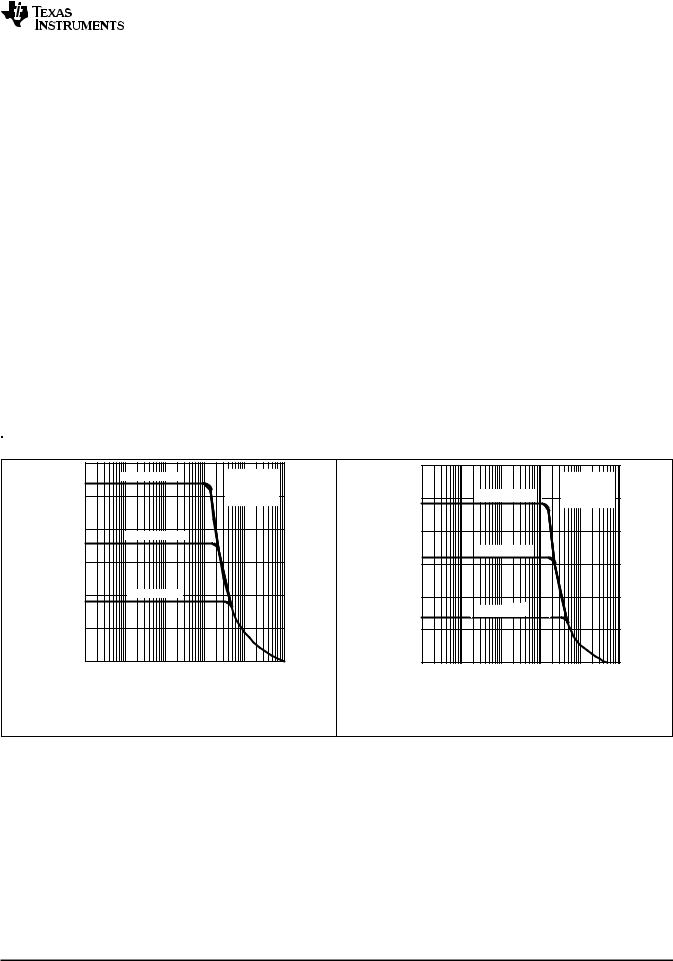
Figure 1. Maximum Peak Output Voltage
vs
Frequency
|
±15 |
|
|
|
|
|
−V |
|
|
|
|
RL = 2 K! |
|
±12.5 |
|
VCC± = ±15 V |
|
TA = 25°C |
|
|
VOLTAGE |
|
|
SEE FIGURE 2 |
|||
|
|
|
|
|
||
OUTPUT |
±10 |
|
VCC± = ±10 V |
|
|
|
|
|
|
|
|
|
|
PEAK |
±7.5 |
|
|
|
|
|
MAXIMUM |
±5 |
|
VCC± = ±5 V |
|
|
|
− |
|
|
|
|
|
|
OMV |
|
|
|
|
|
|
OM |
±2.5 |
|
|
|
|
|
|
|
|
|
|
|
|
|
0 |
|
|
|
|
|
|
100 |
1 K |
10 K |
100 K |
1 M |
10 M |
|
|
|
F − FREQUENCY − HZ |
|
|
|
Figure 2. Maximum Peak Output Voltage
vs
Frequency
Copyright © 1977–2015, Texas Instruments Incorporated |
Submit Documentation Feedback |
9 |
Product Folder Links: TL081 TL081A TL081B TL082 TL082A TL082B TL084 TL084A TL084B

TL081, TL081A, TL081B, TL082, TL082A TL082B, TL084, TL084A, TL084B
SLOS081I –FEBRUARY 1977 –REVISED MAY 2015
|
|
±15 |
|
|
|
|
|
|
|
|
−V |
|
|
|
|
|
|
VCC± = ±15 V |
|
||
±12.5 |
TA = 25°C |
|
|
RL = 2 K! |
|
|
||||
VOLTAGE |
|
|
SEE FIGURE 2 |
|
||||||
|
|
|
|
|
|
|
||||
OUTPUT |
|
|
|
|
|
|
|
|||
|
±10 |
|
|
|
|
|
|
|
|
|
PEAK |
|
|
|
|
|
TA = −55°C |
|
|
|
|
|
±7.5 |
|
|
|
|
|
|
|
|
|
MAXIMUM− |
|
±5 |
TA = 125°C |
|
|
|
|
|
|
|
|
|
|
|
|
|
|
|
|
|
|
OMV |
|
|
|
|
|
|
|
|
|
|
OM |
|
±2.5 |
|
|
|
|
|
|
|
|
|
|
|
|
|
|
|
|
|
|
|
|
|
0 |
|
|
|
|
|
|
|
|
|
|
10 K |
40 K |
100 K |
|
400 K |
1 M |
4 M |
|
10 M |
|
|
|
|
F − FREQUENCY − HZ |
|
|
|
|||
|
|
Figure 3. Maximum Peak Output Voltage |
||||||||
|
|
|
|
|
vs |
|
|
|
|
|
|
|
|
|
Frequency |
|
|
|
|
||
|
|
±15 |
|
|
|
|
|
|
|
|
V |
|
|
VCC± = ±15 V |
|
|
|
|
|
|
|
− |
|
|
TA = 25°C |
|
|
|
|
|
|
|
VOLTAGE |
|
±12.5 |
SEE FIGURE 2 |
|
|
|
|
|
|
|
|
|
|
|
|
|
|
|
|
|
|
OUTPUT |
|
±10 |
|
|
|
|
|
|
|
|
|
|
|
|
|
|
|
|
|
|
|
PEAK |
|
±7.5 |
|
|
|
|
|
|
|
|
MAXIMUM− |
|
±5 |
|
|
|
|
|
|
|
|
|
|
|
|
|
|
|
|
|
|
|
OMV |
|
±2.5 |
|
|
|
|
|
|
|
|
|
|
|
|
|
|
|
|
|
|
|
OM |
|
8 |
|
|
|
|
|
|
|
|
|
|
0 |
0.2 |
0.4 |
0.7 |
1 |
2 |
4 |
7 |
10 |
|
|
0.1 |
||||||||
|
|
|
|
RL − LOAD RESISTANCE − K! |
|
|
|
|||
|
|
Figure 5. Maximum Peak Output Voltage |
||||||||
|
|
|
|
|
vs |
|
|
|
|
|
|
|
|
|
Load Resistance |
|
|
|
|||
|
|
1000 |
|
|
|
|
|
|
|
|
DIFFERENTIALSIGNAL-LARGE |
V/MV−AMPLIFICATION |
400 |
|
|
|
|
|
|
|
|
200 |
|
|
|
|
|
|
|
|
||
|
|
|
|
|
|
|
|
|
|
|
|
|
100 |
|
|
|
|
|
|
|
|
|
|
40 |
|
|
|
|
|
|
|
|
|
VOLTAGE |
20 |
|
|
|
|
|
|
|
|
AA |
4 |
VCC± = ±15 V |
|
|
|
|
|
|
||
− |
|
10 |
|
|
|
|
|
|
|
|
VD |
|
|
|
|
|
|
|
|
|
|
|
|
2 |
VO = ±10 V |
|
|
|
|
|
|
|
|
|
RL = 2 K! |
|
|
|
|
|
|
||
|
|
|
|
|
|
|
|
|
||
1 |
|
|
|
|
|
|
|
|
−75 |
−50 |
−25 |
0 |
25 |
50 |
75 |
100 |
125 |
TA − FREE-AIR TEMPERATURE − °C
Figure 7. Large-Signal Differential Voltage Amplification
vs
Free-Air Temperature
|
www.ti.com |
|
|
±15 |
|
−V |
RL = 10 K! |
|
|
||
VOLTAGE |
±12.5 |
|
RL = 2 K! |
||
OUTPUT |
||
±10 |
||
|
||
PEAK |
±7.5 |
|
MAXIMUM− |
±5 |
|
|
||
OMV |
±2.5 |
|
VCC± = ±15 V |
||
OM |
||
|
SEE FIGURE 2 |
|
0 |
|
|
|
|
|
|
|
|
|
|
|
|
|
|
|
|
|
|
|
|
|
|
|
|
|
|
|
|
|
|
|
|
|
|
|
|
|
−75 |
−50 |
−25 |
0 |
25 |
50 |
75 |
100 |
125 |
|||||||||
|
|
|
|
|
|
TA − FREE-AIR TEMPERATURE − °C |
|
|
|
|
||||||||
|
Figure 4. Maximum Peak Output Voltage |
|||||||||||||||||
|
|
|
|
|
|
|
|
|
vs |
|
|
|
|
|
|
|
|
|
|
|
|
|
|
|
Free-Air Temperature |
|
|
|
|
||||||||
|
±15 |
|
|
|
|
|
|
|
|
|
|
|
|
|
|
|
|
|
|
|
|
|
|
|
|
|
|
|
|
|
|
|
|
|
|
||
−V |
|
|
|
RL = 10 K! |
|
|
|
|
|
|
|
|
|
|
|
|||
|
|
|
TA = 25°C |
|
|
|
|
|
|
|
|
|
|
|
||||
VOLTAGE |
±12.5 |
|
|
|
|
|
|
|
|
|
|
|
|
|
|
|
|
|
|
|
|
|
|
|
|
|
|
|
|
|
|
|
|
|
|
|
|
OUTPUT |
±10 |
|
|
|
|
|
|
|
|
|
|
|
|
|
|
|
|
|
PEAK |
±7.5 |
|
|
|
|
|
|
|
|
|
|
|
|
|
|
|
|
|
MAXIMUM− |
|
|
|
|
|
|
|
|
|
|
|
|
|
|
|
|
|
|
±5 |
|
|
|
|
|
|
|
|
|
|
|
|
|
|
|
|
|
|
OM |
|
|
|
|
|
|
|
|
|
|
|
|
|
|
|
|
|
|
±2.5 |
|
|
|
|
|
|
|
|
|
|
|
|
|
|
|
|
|
|
|
8 |
|
|
|
|
|
|
|
|
|
|
|
|
|
|
|||
OMV |
|
|
|
|
|
|
|
|
|
|
|
|
|
|
|
|
|
|
|
0 |
|
|
|
|
|
|
|
|
|
|
|
|
|
|
|
|
|
|
|
|
|
|
|
|
|
|
|
|
|
|
|
|
|
|
||
|
0 |
2 |
4 |
6 |
8 |
10 |
12 |
14 |
16 |
|||||||||
|VCC±| − SUPPLY VOLTAGE − V
Figure 6. Maximum Peak Output Voltage
vs
Supply Voltage
|
|
106 |
|
|
|
|
|
|
|
|
|
|
|
|
|
|
VCC± = ±5 V TO ±15 V |
|
|
||
|
|
|
|
|
|
RL = 2 K" |
|
|
|
|
– LARGE-SIGNALDIFFERENTIAL |
|
105 |
|
|
|
TA = 25°C |
|
|
|
|
VOLTAGEAMPLIFICATION |
104 |
|
|
|
DIFFERENTIAL |
|
0° |
PHASESHIFT |
||
|
|
|
|
VOLTAGE |
|
|
||||
103 |
|
|
|
AMPLIFICATION |
45° |
|||||
|
|
|
|
|
|
|||||
102 |
|
|
|
|
|
|
90° |
|||
VD |
|
|
|
PHASE SHIFT |
|
|
|
|
|
|
AA |
|
101 |
|
|
|
|
135° |
|
||
|
|
|
|
|
|
|
|
|||
|
|
|
|
|
|
|
|
|
||
|
|
1 |
|
|
|
|
|
|
180° |
|
|
|
1 |
10 |
100 |
1 K |
10 K |
100 K |
1 M |
10 M |
|
|
|
|
|
F − FREQUENCY − HZ |
|
|
|
|||
Figure 8. Large-Signal Differential Voltage Amplification and
Phase Shift
vs
Frequency
10 |
Submit Documentation Feedback |
Copyright © 1977–2015, Texas Instruments Incorporated |
|
Product Folder Links: TL081 TL081A TL081B TL082 TL082A TL082B TL084 TL084A TL084B |
|
www.ti.com |
|
|
|
|
|
|
|
106 |
|
|
|
|
|
V/MV |
|
|
|
|
VCC± =±15 V |
|
105 |
|
|
|
C2 = 3 PF |
|
|
− |
|
|
|
TA = 25°C |
|
|
AMPLIFICATION |
|
|
|
|
|
|
|
|
|
|
SEE FIGURE 3 |
|
|
104 |
|
|
|
|
|
|
|
|
|
|
|
|
|
VOLTAGE |
103 |
|
|
|
|
|
|
|
|
|
|
|
|
DIFFERENTIAL |
102 |
|
|
|
|
|
10 |
|
|
|
|
|
|
− |
|
|
|
|
|
|
|
|
|
|
|
|
|
VD |
|
|
|
|
|
|
A |
1 |
|
|
|
|
|
|
|
|
|
|
|
|
|
100 |
1 K |
10 K |
100 K |
1 M |
10 M |
|
F − FREQUENCY WITH FEED-FORWARD COMPENSATION − HZ |
|||||
Figure 9. Differential Voltage Amplification vs
Frequency with Feed-Forward Compensation
|
2 |
|
|
|
|
|
|
|
|
MA |
|
|
|
|
|
|
VCC± = ±15 V |
|
|
1.8 |
|
|
|
|
|
NO SIGNAL |
|
||
− |
|
|
|
|
|
|
|
||
|
|
|
|
|
|
NO LOAD |
|
||
PERAMPLIFIER |
1.2 |
|
|
|
|
|
|
||
|
1.6 |
|
|
|
|
|
|
|
|
|
1.4 |
|
|
|
|
|
|
|
|
CURRENT |
1 |
|
|
|
|
|
|
|
|
|
|
|
|
|
|
|
|
|
|
SUPPLY− |
0.8 |
|
|
|
|
|
|
|
|
0.6 |
|
|
|
|
|
|
|
|
|
ICC |
0.4 |
|
|
|
|
|
|
|
|
± |
|
|
|
|
|
|
|
|
|
CC |
0.2 |
|
|
|
|
|
|
|
|
I |
|
|
|
|
|
|
|
|
|
|
0 |
|
|
|
|
|
|
|
|
|
−75 |
−50 |
−25 |
0 |
25 |
50 |
75 |
100 |
125 |
|
|
|
TA − FREE-AIR TEMPERATURE − °C |
|
|
||||
Figure 11. Supply Current per Amplifier vs
Free-Air Temperature
|
100 |
|
|
|
|
|
|
|
|
|
V CC± =±15 V |
|
|
|
|
|
|
NA |
10 |
|
|
|
|
|
|
|
CURRENT − |
|
|
|
|
|
|
|
|
|
|
|
|
|
|
|
|
|
− INPUT BIAS |
1 |
|
|
|
|
|
|
|
|
|
|
|
|
|
|
|
|
IB |
0.1 |
|
|
|
|
|
|
|
I |
|
|
|
|
|
|
|
|
|
0.01 |
|
|
|
|
|
|
|
|
− 50 |
− 25 |
0 |
25 |
50 |
75 |
100 |
125 |
|
|
|
TA − FREE-AIR TEMPERATURE − °C |
|
|
|||
Figure 13. Input Bias Current
vs
Free-Air Temperature
|
|
TL081, TL081A, TL081B, TL082, TL082A |
|||||||
|
|
|
TL082B, TL084, TL084A, TL084B |
||||||
|
|
SLOS081I –FEBRUARY 1977–REVISED MAY 2015 |
|||||||
|
250 |
|
|
|
|
|
|
|
|
|
225 |
|
|
|
|
|
VCC± =±15 V |
|
|
|
|
|
|
|
|
NO SIGNAL |
|
||
|
|
|
|
|
|
|
NO LOAD |
|
|
−MW |
200 |
|
|
|
|
|
|
|
|
175 |
|
|
|
|
|
|
|
|
|
DISSIPATION |
|
|
|
|
|
TL084, TL085 |
|||
|
|
|
|
|
|
||||
150 |
|
|
|
|
|
|
|
|
|
125 |
|
|
|
|
|
|
|
|
|
|
|
|
|
|
|
|
|
|
|
POWER |
100 |
|
|
|
|
TL082, TL083 |
|
||
|
|
|
|
|
|
||||
|
|
|
|
|
|
|
|
|
|
TOTAL |
75 |
|
|
|
|
|
|
|
|
|
|
|
|
|
TL081 |
|
|
||
− |
50 |
|
|
|
|
|
|
||
|
|
|
|
|
|
|
|
||
D |
|
|
|
|
|
|
|
|
|
P |
25 |
|
|
|
|
|
|
|
|
|
|
|
|
|
|
|
|
|
|
|
0 |
|
|
|
|
|
|
|
|
|
− 75 |
− 50 |
−25 |
0 |
25 |
50 |
75 |
100 |
125 |
|
|
|
TA − FREE-AIR TEMPERATURE °−C |
|
|
||||
Figure 10. Total Power Dissipation
vs
Free-Air Temperature
|
2 |
|
|
|
|
|
|
|
|
|
|
|
|
|
|
|
|
|
|
|
|
|
|
|
|
|
|
|
|
|
|
|
|
|
|
|
|
MA |
1.8 |
|
TA = 25°C |
|
|
|
|
|
|
|
|
|
|
|
|
|||
|
NO SIGNAL |
|
|
|
|
|
|
|
|
|
|
|
|
|||||
− |
|
|
|
|
|
|
|
|
|
|
|
|
|
|
||||
|
|
NO LOAD |
|
|
|
|
|
|
|
|
|
|
|
|
|
|
||
AMPLIFIER |
1.6 |
|
|
|
|
|
|
|
|
|
|
|
|
|
|
|
||
|
|
|
|
|
|
|
|
|
|
|
|
|
|
|
|
|
||
|
|
|
|
|
|
|
|
|
|
|
|
|
|
|
|
|
|
|
PER |
1.4 |
|
|
|
|
|
|
|
|
|
|
|
|
|
|
|
|
|
|
|
|
|
|
|
|
|
|
|
|
|
|
|
|
|
|
||
1.2 |
|
|
|
|
|
|
|
|
|
|
|
|
|
|
|
|
|
|
CURRENT |
|
|
|
|
|
|
|
|
|
|
|
|
|
|
|
|
|
|
1 |
|
|
|
|
|
|
|
|
|
|
|
|
|
|
|
|
|
|
|
|
|
|
|
|
|
|
|
|
|
|
|
|
|
|
|
|
|
SUPPLY− |
0.8 |
|
|
|
|
|
|
|
|
|
|
|
|
|
|
|
|
|
|
|
|
|
|
|
|
|
|
|
|
|
|
|
|
|
|
||
0.6 |
|
|
|
|
|
|
|
|
|
|
|
|
|
|
|
|
|
|
|
|
|
|
|
|
|
|
|
|
|
|
|
|
|
|
|
|
|
ICC |
0.4 |
|
|
|
|
|
|
|
|
|
|
|
|
|
|
|
|
|
|
|
|
|
|
|
|
|
|
|
|
|
|
|
|
|
|
||
± |
|
|
|
|
|
|
|
|
|
|
|
|
|
|
|
|
|
|
CC |
0.2 |
|
|
|
|
|
|
|
|
|
|
|
|
|
|
|
|
|
I |
|
|
|
|
|
|
|
|
|
|
|
|
|
|
|
|
|
|
|
0 |
|
|
|
|
|
|
|
|
|
|
|
|
|
|
|
|
|
|
|
|
|
|
|
|
|
|
|
|
|
|
|
|
|
|
|
|
|
0 |
2 |
4 |
6 |
8 |
10 |
12 |
14 |
16 |
|||||||||
|VCC±| − SUPPLY VOLTAGE − V
Figure 12. Supply Current per Amplifier vs
Supply Voltage
|
6 |
|
|
|
|
VCC± = ±15 V |
|
|
V |
|
|
|
|
|
|
||
|
|
|
|
|
RL = 2 K! |
|
||
− |
|
|
|
|
|
|
||
VOLTAGES |
4 |
|
|
|
|
CL = 100 PF |
|
|
|
|
OUTPUT |
|
TA = 25°C |
|
|||
|
|
|
|
|
|
|||
|
|
|
|
|
|
|
|
|
OUTPUT |
2 |
|
|
|
|
|
|
|
|
|
|
|
|
|
|
|
|
INPUTAND |
0 |
|
|
|
|
|
|
|
−2 |
|
|
|
|
|
|
|
|
− |
|
|
|
|
|
|
|
|
|
|
|
|
|
|
|
|
|
O |
|
|
|
INPUT |
|
|
|
|
V |
|
|
|
|
|
|
|
|
|
|
|
|
|
|
|
|
|
AND |
−4 |
|
|
|
|
|
|
|
|
|
|
|
|
|
|
|
|
I |
|
|
|
|
|
|
|
|
V |
|
|
|
|
|
|
|
|
|
−6 |
|
|
|
|
|
|
|
|
0 |
0.5 |
1 |
1.5 |
2 |
2.5 |
3 |
3.5 |
|
|
T − TIME − µS |
|
|
|
|
||
Figure 14. Voltage-Follower Large-Signal Pulse Response
Copyright © 1977–2015, Texas Instruments Incorporated |
Submit Documentation Feedback |
11 |
Product Folder Links: TL081 TL081A TL081B TL082 TL082A TL082B TL084 TL084A TL084B |
|
|
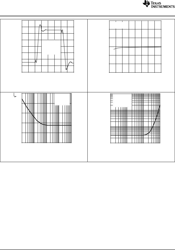
TL081, TL081A, TL081B, TL082, TL082A |
|
|
|
|
|
|
|
|
|
|
|
|||||
TL082B, TL084, TL084A, TL084B |
|
|
|
|
|
|
|
|
|
|
|
|
|
|||
SLOS081I –FEBRUARY 1977 –REVISED MAY 2015 |
|
|
|
|
|
|
|
|
|
|
|
www.ti.com |
||||
|
28 |
|
|
|
|
|
|
|
89 |
|
|
|
|
|
|
|
|
|
|
|
|
|
|
|
DB |
VCC± =±15 V |
|
|
|
|
|
|
|
|
24 |
|
|
|
|
|
|
RL = 10 KΩ |
|
|
|
|
|
|
||
|
|
|
|
|
|
|
|
− |
88 |
|
|
|
|
|
|
|
|
|
|
|
|
|
|
|
-MODEREJECTIONRATIO |
|
|
|
|
|
|
|
|
OUTPUTVOLTAGE−MV |
20 |
|
|
|
|
|
|
|
|
|
|
|
|
|
|
|
16 |
|
|
|
|
|
|
87 |
|
|
|
|
|
|
|
||
|
VCC± =±15 V |
|
|
|
|
|
|
|
|
|
|
|
||||
|
|
|
|
|
|
|
|
|
|
|
|
|
||||
12 |
|
RL = 2 KΩ |
|
|
|
|
|
|
|
|
|
|
|
|||
|
CL = 100 PF |
|
|
|
86 |
|
|
|
|
|
|
|
||||
|
|
TA = 25°C |
|
|
|
|
|
|
|
|
|
|
|
|||
8 |
|
SEE FIGURE 1 |
|
|
|
|
|
|
|
|
|
|
|
|||
− |
|
|
|
|
|
|
|
COMMON |
85 |
|
|
|
|
|
|
|
O |
|
|
|
|
|
|
|
|
|
|
|
|
|
|
||
|
|
|
|
|
|
|
|
|
|
|
|
|
|
|
||
V |
4 |
|
|
|
|
|
|
|
|
|
|
|
|
|
|
|
|
|
|
|
|
|
|
|
|
|
|
|
|
|
|
||
|
|
|
|
|
|
|
|
− |
84 |
|
|
|
|
|
|
|
|
0 |
|
|
|
|
|
|
CMRR |
|
|
|
|
|
|
|
|
|
|
|
|
|
|
|
|
|
|
|
|
|
|
|
||
|
|
|
|
|
|
|
|
|
|
|
|
|
|
|
|
|
|
− 4 |
|
|
|
|
|
|
|
83 |
|
|
|
|
|
|
|
|
0 |
0.2 |
0.4 |
0.6 |
0.8 |
1.0 |
1.2 |
|
− 75 |
− 50 − 25 |
0 |
25 |
50 |
75 |
100 |
125 |
|
T − ELAPSED TIME – µS |
|
|
|
|
|
|
|
|
|
° |
|
|
|||
|
|
|
|
|
|
|
|
|
|
TA − FREE-AIR TEMPERATURE −C |
|
|
||||
Figure 15. Output Voltage |
Figure 16. Common-Mode Rejection Ratio |
vs |
vs |
Elapsed Time |
Free-Air Temperature |
HZ |
50 |
|
|
|
VCC± = ±15 V |
|
1 |
VCC± = ±15 V |
|
|
|
||||
|
|
|
|
|
|
|
|
|
|||||||
NV/HZ |
|
|
|
|
% |
0.4 |
|
|
|
||||||
|
|
|
|
RS = 20 ! |
V |
|
= 6 V |
|
|
|
|||||
|
|
|
|
|
AVD = 10 |
|
|
AVD |
= 1 |
|
|
|
|
|
|
− |
40 |
|
|
|
TA = 25°C |
− |
|
I(RMS) |
|
|
|
|
|
||
|
|
|
|
|
|
|
|
|
|
|
|||||
NOISEINPUTVOLTAGE |
|
|
|
DISTORTIONHARMONIC |
|
TA = 25°C |
|
|
|
|
|||||
|
|
|
|
|
|
|
|
|
|
|
|||||
20 |
|
|
|
|
|
0.1 |
|
|
|
|
|
|
|
||
|
|
|
|
|
|
|
|
|
|
|
|
|
|
|
|
|
30 |
|
|
|
|
|
|
|
|
|
|
|
|
|
|
EQUIVALENT− |
|
|
|
|
|
|
TOTAL−THD |
0.04 |
|
|
|
|
|
|
|
|
|
|
|
|
|
0.01 |
|
|
|
|
|
|
|
||
|
10 |
|
|
|
|
|
|
0.004 |
|
|
|
|
|
|
|
N |
|
|
|
|
|
|
|
|
|
|
|
|
|
|
|
V |
|
|
|
|
|
|
|
|
|
|
|
|
|
|
|
|
0 |
|
|
|
|
|
|
0.001 |
|
|
|
|
|
|
|
|
10 |
40 |
100 |
400 1 K |
4 K 10 K |
40 K 100 K |
|
100 |
400 |
1 K |
4 K |
10 K |
40 K 100 K |
||
|
|
|
|
F − FREQUENCY − HZ |
|
|
|
|
|
|
F − FREQUENCY − HZ |
|
|||
Figure 17. Equivalent Input Noise Voltage |
Figure 18. Total Harmonic Distortion |
vs |
vs |
Frequency |
Frequency |
12 |
Submit Documentation Feedback |
Copyright © 1977–2015, Texas Instruments Incorporated |
|
Product Folder Links: TL081 TL081A TL081B TL082 TL082A TL082B TL084 TL084A TL084B |
|
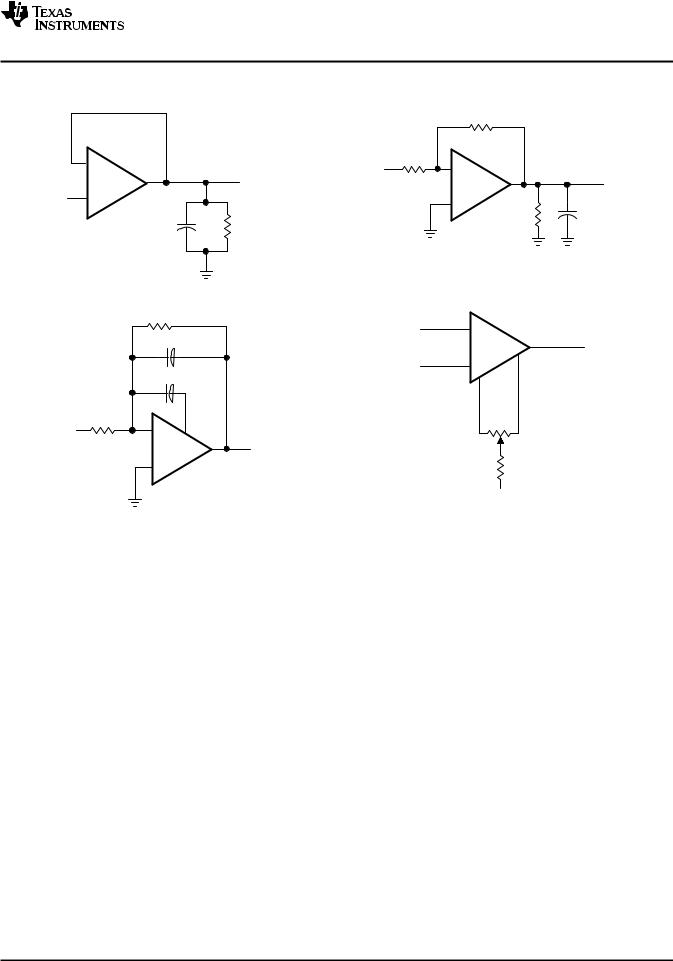
www.ti.com
7 Parameter Measurement Information
− |
|
|
OUT |
+ |
|
VI |
|
CL = 100 PF |
RL = 2 KΩ |
TL081, TL081A, TL081B, TL082, TL082A TL082B, TL084, TL084A, TL084B
SLOS081I –FEBRUARY 1977–REVISED MAY 2015
|
10 KΩ |
|
|
1 KΩ |
|
VI |
− |
|
|
|
|
|
|
OUT |
|
+ |
CL = 100 PF |
|
RL |
Figure 19. Test Figure 1 |
Figure 20. Test Figure 2 |
100KΩ
C2
|
C1 |
500 PF |
IN − |
− |
N1 |
|
|
OUT |
|
+ |
|
Figure 21. Test Figure 3
IN −
IN +
|
TL081 |
− |
|
|
OUT |
+ |
N2 |
N1
100 KΩ
1.5 KΩ
VCC −
Figure 22. Test Figure 4
Copyright © 1977–2015, Texas Instruments Incorporated |
Submit Documentation Feedback |
13 |
Product Folder Links: TL081 TL081A TL081B TL082 TL082A TL082B TL084 TL084A TL084B |
|
|
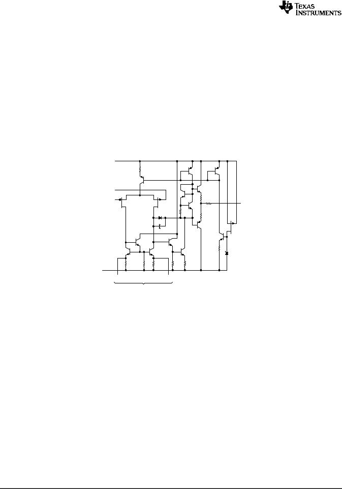
TL081, TL081A, TL081B, TL082, TL082A
TL082B, TL084, TL084A, TL084B
SLOS081I –FEBRUARY 1977 –REVISED MAY 2015 |
www.ti.com |
8 Detailed Description
8.1 Overview
The TL08xx JFET-input operational amplifier family is designed to offer a wider selection than any previously developed operational amplifier family. Each of these JFET-input operational amplifiers incorporates wellmatched, high-voltage JFET and bipolar transistors in a monolithic integrated circuit. The devices feature high slew rates, low input bias and offset currents, and low offset-voltage temperature coefficient. Offset adjustment and external compensation options are available within the TL08xx family.
The C-suffix devices are characterized for operation from 0°C to 70°C. The I-suffix devices are characterized for operation from −40°C to 85°C. The Q-suffix devices are characterized for operation from –40°C to +125°C. The M-suffix devices are characterized for operation over the full military temperature range of −55°C to +125°C.
8.2 Functional Block Diagram
VCC +
IN +
64Ω
IN −
OUT
128Ω
64Ω
C1
1080Ω |
1080Ω |
VCC − |
|
OFFSET N1 |
OFFSET N2 |
|
TL081 ONLY |
8.3 Feature Description
8.3.1 Total Harmonic Distortion
Harmonic distortions to an audio signal are created by electronic components in a circuit. Total harmonic distortion (THD) is a measure of harmonic distortions accumulated by a signal in an audio system. These devices have a very low THD of 0.003% meaning that the TL08x devices will add little harmonic distortion when used in audio signal applications.
8.3.2 Slew Rate
The slew rate is the rate at which an operational amplifier can change its output when there is a change on the input. These devices have a 13-V/μs slew rate.
8.4 Device Functional Modes
These devices are powered on when the supply is connected. This device can be operated as a single-supply operational amplifier or dual-supply amplifier depending on the application.
14 |
Submit Documentation Feedback |
Copyright © 1977–2015, Texas Instruments Incorporated |
|
Product Folder Links: TL081 TL081A TL081B TL082 TL082A TL082B TL084 TL084A TL084B |
|
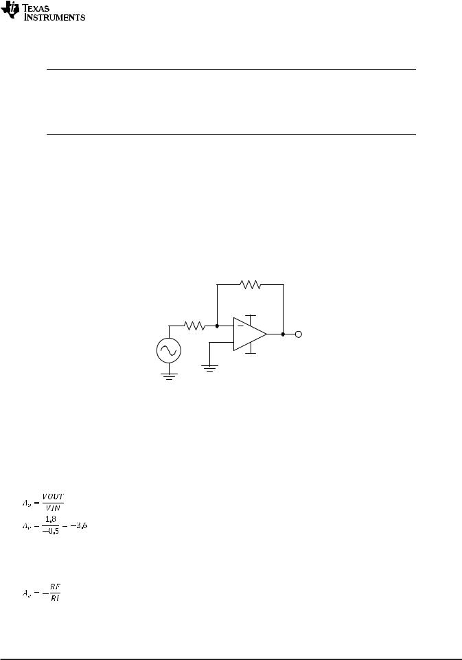
TL081, TL081A, TL081B, TL082, TL082A
TL082B, TL084, TL084A, TL084B
www.ti.com |
SLOS081I –FEBRUARY 1977–REVISED MAY 2015 |
9 Applications and Implementation
NOTE
Information in the following applications sections is not part of the TI component specification, and TI does not warrant its accuracy or completeness. TI’s customers are responsible for determining suitability of components for their purposes. Customers should validate and test their design implementation to confirm system functionality.
9.1 Application Information
The TL08x series of operational amplifiers can be used in countless applications. The few applications in this section show principles used in all applications of these parts.
9.2 Typical Applications
9.2.1 Inverting Amplifier Application
A typical application for an operational amplifier in an inverting amplifier. This amplifier takes a positive voltage on the input, and makes it a negative voltage of the same magnitude. In the same manner, it also makes negative voltages positive.
RF
RI Vsup+
VOUT
+
VIN
Vsup-
Figure 23. Schematic for Inverting Amplifier Application
9.2.1.1 Design Requirements
The supply voltage must be chosen such that it is larger than the input voltage range and output range. For instance, this application will scale a signal of ±0.5 V to ±1.8 V. Setting the supply at ±12 V is sufficient to accommodate this application.
9.2.1.2 Detailed Design Procedure
Determine the gain required by the inverting amplifier:
(1)
(2)
Once the desired gain is determined, choose a value for RI or RF. Choosing a value in the kΩ range is desirable because the amplifier circuit will use currents in the milliamp range. This ensures the part will not draw too much current. This example will choose 10 kΩ for RI which means 36 kΩ will be used for RF. This was determined by Equation 3.
(3)
Copyright © 1977–2015, Texas Instruments Incorporated |
Submit Documentation Feedback |
15 |
Product Folder Links: TL081 TL081A TL081B TL082 TL082A TL082B TL084 TL084A TL084B |
|
|
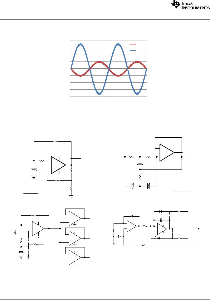
TL081, TL081A, TL081B, TL082, TL082A
TL082B, TL084, TL084A, TL084B
SLOS081I –FEBRUARY 1977 –REVISED MAY 2015 www.ti.com
Typical Applications (continued)
9.2.1.3 Application Curve
|
2 |
|
|
|
|
|
|
|
|
|
VIN |
1.5 |
|
|
|
|
|
|
|
|
|
|
VOUT |
|
1 |
|
|
|
|
0.5 |
|
|
|
|
|
VOLTS |
0 |
|
|
|
|
|
|
|
|
|
|
-0.5 |
|
|
|
|
|
|
-1 |
|
|
|
|
-1.5 |
|
|
|
|
|
|
-2 |
|
|
|
|
|
0 |
0.5 |
1 |
1.5 |
2 |
|
|
|
TIME (MS) |
|
|
Figure 24. Input and output voltages of the inverting amplifier
9.3 System Examples
9.3.1 General Applications
CF = 3.3 µF
RF = 100 KΩ
15 V
3.3 KΩ −
TL081 +
− 15 V
OUTPUT |
INPUT |
|
1 KΩ
3.3 KΩ
9.1 KΩ
1
F =
2π RF CF
Figure 25. 0.5-Hz Square-Wave Oscillator
|
|
VCC + |
|
|
|
|
− |
|
|
R1 |
R2 |
TL081 |
|
|
|
|
OUTPUT |
||
|
|
+ |
|
|
C3 |
|
VCC − |
|
|
|
|
|
|
|
R3 |
|
R1 = R2 = 2(R3) = 1.5 MΩ |
||
C1 |
C2 |
C1 = C2 = |
C3 |
= 110 PF |
|
|
|||
|
|
|
2 |
|
|
|
1 |
|
= 1 KHZ |
|
|
FO = |
|
|
|
|
2π R1 C1 |
|
|
Figure 26. High-Q Notch Filter
|
|
VCC + |
|
|
6 SIN ωT |
1N4148 |
|
|
|
|
|
|
|
− 15 V |
|
|
1 MΩ |
− |
|
18 PF |
|
18 KΩ |
|
|
|
|
|
|
1 KΩ (SEE NOTE A) |
||
|
|
TL084 |
OUTPUT A |
|
|
18 PF |
|
|
VCC + |
|
|
|
|
||
|
+ |
|
|
VCC + |
|
|
|
|
|
|
− |
|
VCC+ |
|
|
|
|
|
|
88.4 KΩ |
|
||
|
+ |
|
|
1/2 |
|
||
|
|
|
− |
|
|||
|
|
|
|
TL082 |
|
||
1 µF |
|
|
|
1/2 |
|
||
TL084 |
|
|
+ |
|
6 COS ωT |
||
VCC + |
88.4 KΩ |
|
TL082 |
||||
INPUT |
− |
|
VCC − |
+ |
|
||
|
|
|
18 PF |
|
VCC − |
1 KΩ |
|
|
|
− |
|
|
|||
|
|
TL084 |
OUTPUT B |
|
|
|
15 V |
100 KΩ |
100 KΩ |
+ |
|
|
|
1N4148 |
18 KΩ |
|
|
|
|
88.4 KΩ |
|
(SEE NOTE A) |
|
|
|
VCC + |
|
|
|
||
|
100 KΩ |
|
|
|
|
|
|
|
|
A. These resistor values may be adjusted for a symmetrical output. |
|||||
100 µF |
100 KΩ |
VCC + |
|||||
|
|
|
|
|
|
||
|
|
− |
|
|
|
|
|
|
|
TL084 |
OUTPUT C |
|
|
|
|
|
|
+ |
|
|
|
|
|
Figure 27. Audio-Distribution Amplifier |
Figure 28. 100-kHz Quadrature Oscillator |
||||||
16 |
Submit Documentation Feedback |
Copyright © 1977–2015, Texas Instruments Incorporated |
|
Product Folder Links: TL081 TL081A TL081B TL082 TL082A TL082B TL084 TL084A TL084B |
|
Loading...