


TLC541MN
Texas Instruments TLC541MN, TLC541IN, TLC541IFNR, TLC541IFN, TLC541IDWR Datasheet
...
TLC540I, TLC541I
8-BIT ANALOG-TO-DIGITAL CONVERTERS
WITH SERIAL CONTROL AND 11 INPUTS
SLAS065A – OCTOBER 1983 – REVISED MARCH 1995
1
POST OFFICE BOX 655303 • DALLAS, TEXAS 75265
D
8-Bit Resolution A/D Converter
D
Microprocessor Peripheral or Stand-Alone
Operation
D
On-Chip 12-Channel Analog Multiplexer
D
Built-in Self-Test Mode
D
Software-Controllable Sample and Hold
D
T otal Unadjusted Error... ±0.5 LSB Max
D
TLC541 is Direct Replacement for Motorola
MC145040 and National Semiconductor
ADC0811. TLC540 is Capable of Higher
Speed
D
Pinout and Control Signals Compatible
with TLC1540 Family of 10-Bit A/D
Converters
D
CMOS Technology
PARAMETER TLC540
TLC541
Channel Acquisition Sample Time
Conversion Time (Max)
Samples per Second (Max)
Power Dissipation (Max)
2 µs
9 µs
75 x 10
3
12.5 mW
3.6 µs
17 µs
40 x 10
3
12.5 mW
description
The TLC540 and TLC541 are CMOS A/D
converters built around an 8-bit switchedcapacitor successive-approximation A/D
converters. They are designed for serial interface
to a microprocessor or peripheral via a 3-state
output with up to four control inputs, including
independent SYSTEM CLOCK, I/O CLOCK, chip
select (CS
), and ADDRESS INPUT. A 4-MHz
system clock for the TLC540 and a 2.1-MHz
system clock for the TLC541 with a design that
includes simultaneous read/write operation allow high-speed data transfers and sample rates of up to
75,180samples per second for the TLC540 and 40,000 samples per second for the TLC541. In addition to the
high-speed converter and versatile control logic, there is an on-chip 12-channel analog multiplexer that can be
used to sample any one of 11 inputs or an internal self-test voltage, and a sample-and-hold that can operate
automatically or under microprocessor control. Detailed information on interfacing to most popular
microprocessors is readily available from the factory.
AVAILABLE OPTIONS
PACKAGE
T
A
SO PLASTIC DIP
(DW)
PLASTIC DIP
(N)
CHIP CARRIER
(FN)
–40°C to 85°C
—
TLC541IDW
TLC540IN
TLC541IN
TLC540IFN
TLC541IFN
–55°C to 125°C — TLC541MN —
Copyright 1995, Texas Instruments Incorporated
PRODUCTION DATA information is current as of publication date.
Products conform to specifications per the terms of Texas Instruments
standard warranty. Production processing does not necessarily include
testing of all parameters.
1
2
3
4
5
6
7
8
9
10
20
19
18
17
16
15
14
13
12
11
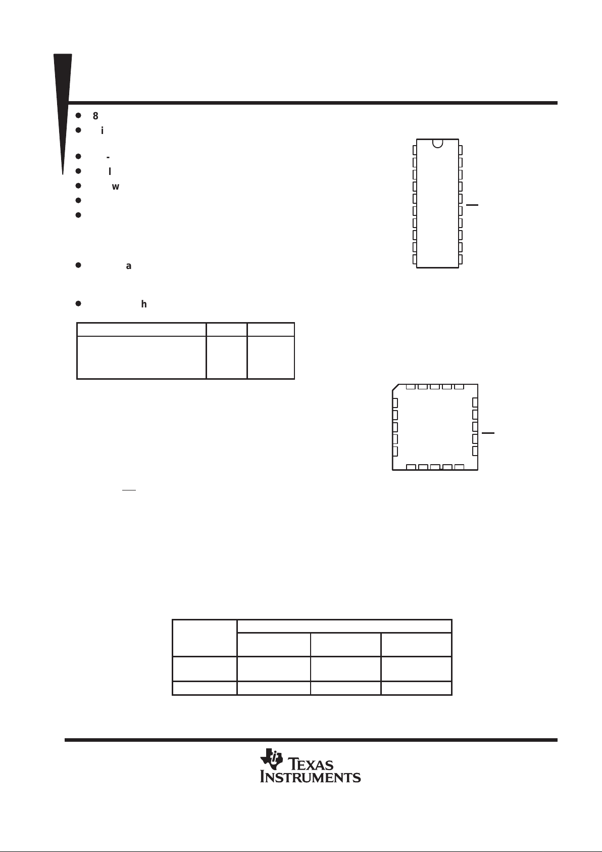
INPUT A0
INPUT A1
INPUT A2
INPUT A3
INPUT A4
INPUT A5
INPUT A6
INPUT A7
INPUT A8
GND
V
CC
SYSTEM CLOCK
I/O CLOCK
ADDRESS INPUT
DATA OUT
CS
REF+
REF–
INPUT A10
INPUT A9
DW OR N PACKAGE
(TOP VIEW)
3 2 1 20 19
910111213
4
5
6
7
8
18
17
16
15
14
I/O CLOCK
ADDRESS INPUT
DATA OUT
CS
REF+
INPUT A3
INPUT A4
INPUT A5
INPUT A6
INPUT A7
FN PACKAGE
(TOP VIEW)
INPUT A2
INPUT A1
INPUT A0
INPUT A10
REF–
SYSTEM CLOCK
INPUT A8
GND
INPUT A9
V
CC

TLC540I, TLC541I
8-BIT ANALOG-TO-DIGITAL CONVERTERS
WITH SERIAL CONTROL AND 11 INPUTS
SLAS065A – OCTOBER 1983 – REVISED MARCH 1995
2
POST OFFICE BOX 655303 • DALLAS, TEXAS 75265
The converters incorporated in the TLC540 and TLC541 feature differential high-impedance reference inputs
that facilitate ratiometric conversion, scaling, and analog circuitry isolation from logic and supply noises. A
switched-capacitor design allows low-error (± 0.5 LSB) conversion in 9 µs for the TLC540 and 17 µs for the
TLC541 over the full operating temperature range.
The TLC540I and TLC541I are characterized for operation from –40°C to 85°C.The TLC541M is characterized
for operation from –55°C to 125°C.
functional block diagram
1
2
3
4
5
6
7
8
9
11
12
SYSTEM
CLOCK
CS
I/O
CLOCK
ADDRESS
INPUT
8-Bit
Analog-to-Digital
Converter
(Switched-Capacitors)
8
4
2
4
4
8
REF–REF+
DATA
OUT
8-to-1 Data
Selector
and Driver
Control Logic
and I/O
Counters
Output
Data
Register
Input
Multiplexer
Self-Test
Reference
Input
Address
Register
Sample
and
Hold
12-Channel
Analog
Multiplexer
Analog
Inputs
A0
A1
A2
A3
A4
A5
A6
A7
A8
A9
A10
14 13
16
17
18
15
19
typical equivalent inputs
INPUT CIRCUIT IMPEDANCE DURING SAMPLING MODE INPUT CIRCUIT IMPEDANCE DURING HOLD MODE
1 kΩ TYP
Ci = 60 pF TYP
(equivalent input
capacitance)
5 MΩ TYP
INPUT
A0–A10
INPUT
A0–A10
TLC540I, TLC541I
8-BIT ANALOG-TO-DIGITAL CONVERTERS
WITH SERIAL CONTROL AND 11 INPUTS
SLAS065A – OCTOBER 1983 – REVISED MARCH 1995
3
POST OFFICE BOX 655303 • DALLAS, TEXAS 75265
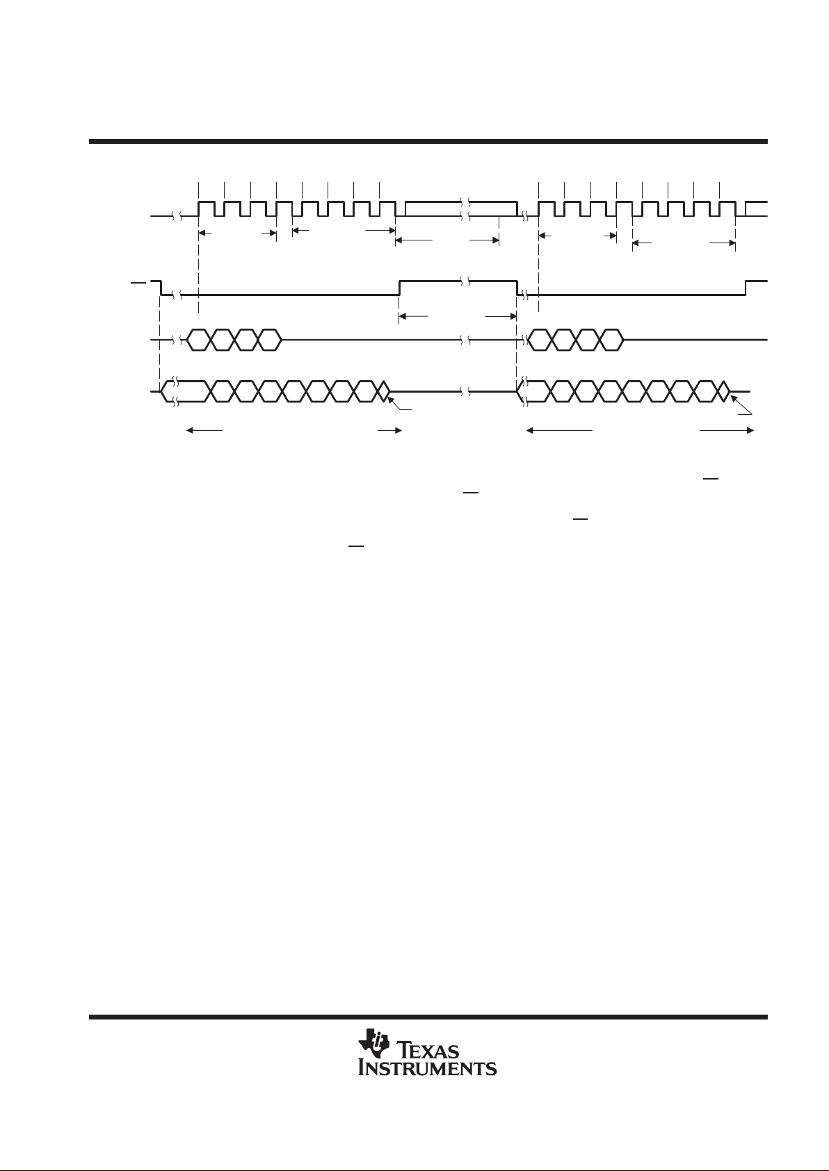
operating sequence
ADDRESS
INPUT
Hi-Z
B7
B0B1B2B3B4B5B6B7
C3 C2 C1 C0
LSBMSB
Conversion Data B
MSBMSB LSB
Hi-Z State
Don’t Care
MSBLSBMSB
(See Note B)
A7
A7 A6 A5 A4 A3 A2 A1 A0
State
LSB
B0B1B2
MSB
B3
Don’t Care
1
1
Sample
Cycle C
Access
Cycle C
See Note A
t
conv
Sample
Cycle B
Access
Cycle B
(see Note C)
88765432765432
I/O
CLOCK
CS
DATA
OUT
Don’t Care
t
wH(CS)
Previous Conversion Data A
NOTES: A. The conversion cycle, which requires 36 system clock periods, is initiated on the 8th falling edge of I/O CLOCK after CS goes low
for the channel whose address exists in memory at that time. If CS
is kept low during conversion, I/O CLOCK must remain low
for at least 36 system clock cycles to allow conversion to be completed.
B. The most significant bit (MSB) will automatically be placed on the DAT A OUT bus after CS
is brought low. The remaining seven
bits (A6–A0) will be clocked out on the first seven I/O CLOCK falling edges.
C. To minimize errors caused by noise at CS
, the internal circuitry waits for three system clock cycles (or less) after a chip select
falling edge is detected before responding to control input signals. Therefore, no attempt should be made to clock-in address data
until the minimum chip-select setup time has elapsed.
absolute maximum ratings over operating free-air temperature range (unless otherwise noted)
†
Supply voltage, V
CC
(see Note 1) 6.5 V. . . . . . . . . . . . . . . . . . . . . . . . . . . . . . . . . . . . . . . . . . . . . . . . . . . . . . . . . . .
Input voltage range, V
I
(any input) –0.3 V to VCC +0.3 V. . . . . . . . . . . . . . . . . . . . . . . . . . . . . . . . . . . . . . . . . . . .
Output voltage range, V
O
–0.3 V to VCC +0.3 V. . . . . . . . . . . . . . . . . . . . . . . . . . . . . . . . . . . . . . . . . . . . . . . . . . . .
Peak input current range (any input) ±10 mA. . . . . . . . . . . . . . . . . . . . . . . . . . . . . . . . . . . . . . . . . . . . . . . . . . . . . . .
Peak total input current (all inputs) ±30 mA. . . . . . . . . . . . . . . . . . . . . . . . . . . . . . . . . . . . . . . . . . . . . . . . . . . . . . . . .
Operating free-air temperature range, T
A
: TLC540I, TLC541I –40°C to 85°C. . . . . . . . . . . . . . . . . . . . . . . . . .
Storage temperature range, T
stg
–65°C to 150°C. . . . . . . . . . . . . . . . . . . . . . . . . . . . . . . . . . . . . . . . . . . . . . . . . . . .
Case temperature for 10 seconds: FN package 260°C. . . . . . . . . . . . . . . . . . . . . . . . . . . . . . . . . . . . . . . . . . . . . . .
Lead temperature 1,6 mm (1/16 inch) from case for 10 seconds: DW or N package 260°C. . . . . . . . . . . . . . .
†
Stresses beyond those listed under “absolute maximum ratings” may cause permanent damage to the device. These are stress ratings only, and
functional operation of the device at these or any other conditions beyond those indicated under “recommended operating conditions” is not
implied. Exposure to absolute-maximum-rated conditions for extended periods may affect device reliability.
NOTE 1: All voltage values are with respect to digital ground with REF– and GND wired together (unless otherwise noted).
TLC540I, TLC541I
8-BIT ANALOG-TO-DIGITAL CONVERTERS
WITH SERIAL CONTROL AND 11 INPUTS
SLAS065A – OCTOBER 1983 – REVISED MARCH 1995
4
POST OFFICE BOX 655303 • DALLAS, TEXAS 75265
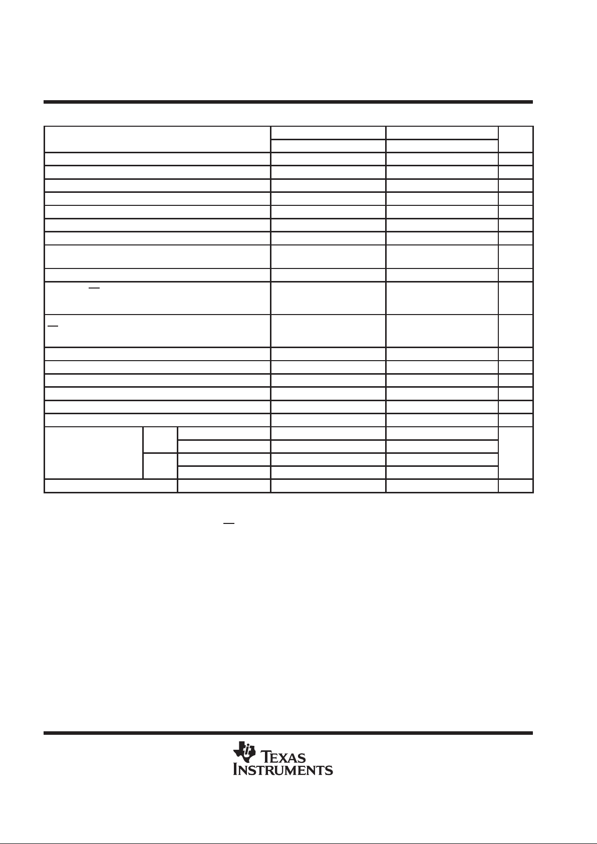
recommended operating conditions
TLC540 TLC541
MIN NOM MAX MIN NOM MAX
UNIT
Supply voltage, V
CC
4.75 5 5.5 4.75 5 5.5 V
Positive reference voltage, V
ref+
(see Note 2) 2.5 VCCVCC+0.1 2.5 V
CCVCC
+0.1 V
Negative reference voltage, V
ref–
(see Note 2) –0.1 0 2.5 – 0.1 0 2.5 V
Differential reference voltage, V
ref+
– V
ref–
(see Note 2) 1 VCCVCC+0.2 1 V
CCVCC
+0.2 V
Analog input voltage (see Note 2) 0 V
CC
0 V
CC
V
High-level control input voltage, V
IH
2 2 V
Low-level control input voltage, V
IL
0.8 0.8 V
Setup time, address bits at data input before I/O CLOCK↑,
t
su(A)
200 400 ns
Hold time, address bits after I/O CLOCK↑,t
h(A)
0 0 ns
Setup time, CS low before clocking in first address bit, t
su(CS)
(see Note 3)
3 3
System
clock
cycles
CS high during conversion, t
wH(CS)
36 36
System
clock
cycles
I/O CLOCK frequency, f
clock(I/O)
0 2.048 0 1.1 MHz
Pulse duration, SYSTEM CLOCK frequency, f
clock(SYS)
f
clock(I/O)
4 f
clock(I/O)
2.1 MHz
Pulse duration, SYSTEM CLOCK high, t
wH(SYS)
110 210 MHz
Pulse duration, SYSTEM CLOCK low, t
wL(SYS)
100 190 MHz
Pulse duration, I/O clock high, t
wH(I/O)
200 404 ns
Pulse duration, I/O clock low, t
wL(I/O)
200 404 ns
f
clock(SYS)
≤ 1048 kHz 30 30
Clock transition time
System
f
clock(SYS)
> 1048 kHz 20 20
(see Note 4)
f
clock(I/O)
≤ 525 kHz 100 100
ns
I/O
f
clock(I/O)
> 525 kHz 40 40
Operating free-air temperature, TATLC540I, TLC541I –40 85 –40 85 °C
NOTES: 2. Analog input voltages greater than that applied to REF + convert as all “1”s (11111111), while input voltages less than that applied
to REF– convert as all “0”s (00000000). For proper operation, REF+ voltage must be at least 1 V higher than REF– voltage. Also,
the total unadjusted error may increase as this differential reference voltage falls below 4.75 V.
3. To minimize errors caused by noise at CS
, the internal circuitry waits for three SYSTEM CLOCK cycles (or less) after a chip select
falling edge is detected before responding to control input signals. Therefore, no attempt should be made to clock in an address until
the minimum chip select setup time has elapsed.
4. This is the time required for the clock input signal to fall from VIH min to VIL max or to rise from VIL max to VIH min. In the vicinity
of normal room temperature, the devices function with input clock transition time as slow as 2 µs for remote data acquisition
applications where the sensor and the A/D converter are placed several feet away from the controlling microprocessor.
 Loading...