


Texas Instruments TL084CD, TL084CJ, TL084BCN, TL084ID, TL084CPWR Datasheet
...TL081, TL081A, TL081B, TL082, TL082A, TL082B TL082Y, TL084, TL084A, TL084B, TL084Y JFET-INPUT OPERATIONAL AMPLIFIERS
SLOS081E ± FEBRUARY 1977 ± REVISED FEBRUARY 1999
D D
D D D
Low Power Consumption |
D High Input Impedance . . . JFET-Input Stage |
Wide Common-Mode and Differential |
D Latch-Up-Free Operation |
Voltage Ranges |
D High Slew Rate . . . 13 V/μs Typ |
Low Input Bias and Offset Currents |
D Common-Mode Input Voltage Range |
|
|
Output Short-Circuit Protection |
Includes VCC+ |
Low Total Harmonic |
|
Distortion . . . 0.003% Typ |
|
description
The TL08x JFET-input operational amplifier family is designed to offer a wider selection than any previously developed operational amplifier family. Each of these JFET-input operational amplifiers incorporates well-matched, high-voltage JFET and bipolar transistors in a monolithic integrated circuit. The devices feature high slew rates, low input bias and offset currents, and low offset voltage temperature coefficient. Offset adjustment and external compensation options are available within the TL08x family.
The C-suffix devices are characterized for operation from 0°C to 70°C. The I-suffix devices are characterized for operation from ±40°C to 85°C. The Q-suffix devices are characterized for operation from ±40°C to 125°C. The M-suffix devices are characterized for operation over the full military temperature range of ±55°C to 125°C.
symbols
|
TL081 |
|
TL082 (EACH AMPLIFIER) |
||||||||
|
|
|
|
|
|
|
TL084 (EACH AMPLIFIER) |
||||
OFFSET N1 |
|
|
|
|
|
|
|
|
|
|
|
|
+ |
|
|
|
|
|
|
|
|
|
|
IN + |
|
|
|
OUT |
IN + |
|
|
|
OUT |
||
|
|
|
|
|
+ |
|
|||||
|
|
|
|||||||||
|
|
|
|
|
|||||||
IN ± |
|
± |
|
|
IN ± |
|
|
± |
|
||
|
|
|
|
|
|
||||||
|
|
|
|
|
|
|
|
||||
|
|||||||||||
|
|
|
|
|
|
||||||
OFFSET N2 |
|
|
|
|
|
|
|
|
|
|
|
|
|
|
|
|
|
|
|
|
|
|
|
|
|
|
|
|
|
|
|
|
|
|
|
Please be aware that an important notice concerning availability, standard warranty, and use in critical applications of Texas Instruments semiconductor products and disclaimers thereto appears at the end of this data sheet.
PRODUCTION DATA information is current as of publication date. Products conform to specifications per the terms of Texas Instruments standard warranty. Production processing does not necessarily include testing of all parameters.
Copyright 1999, Texas Instruments Incorporated
On products compliant to MIL-PRF-38535, all parameters are tested unless otherwise noted. On all other products, production processing does not necessarily include testing of all parameters.
POST OFFICE BOX 655303 •DALLAS, TEXAS 75265 |
1 |
TL081, TL081A, TL081B, TL082, TL082A, TL082B TL082Y, TL084, TL084A, TL084B, TL084Y JFET-INPUT OPERATIONAL AMPLIFIERS
SLOS081E ± FEBRUARY 1977 ± REVISED FEBRUARY 1999
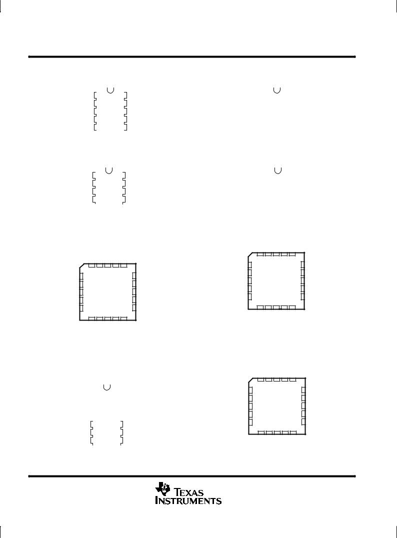
TL081M
U PACKAGE (TOP VIEW)
NC |
1 |
10 |
NC |
OFFSET N1 |
2 |
9 |
NC |
IN± |
3 |
8 |
VCC+ |
IN+ |
4 |
7 |
OUT |
VCC± |
5 |
6 |
OFFSET N2 |
TL081, TL081A, TL081B D, JG, P, OR PW PACKAGE (TOP VIEW)
OFFSET N1 |
1 |
8 |
NC |
IN± |
2 |
7 |
VCC + |
IN+ |
3 |
6 |
OUT |
VCC ± |
4 |
5 |
OFFSET N2 |
TL081M . . . FK PACKAGE
(TOP VIEW)
|
NC |
OFFSET N1 |
NC |
NC |
NC |
|
NC |
3 |
2 |
1 |
20 19 |
NC |
|
4 |
|
|
|
18 |
||
IN± |
5 |
|
|
|
17 |
VCC + |
NC |
6 |
|
|
|
16 |
NC |
IN+ |
7 |
|
|
|
15 |
OUT |
NC |
8 |
|
|
|
14 |
NC |
|
9 |
10 11 12 13 |
|
|||
NC CC± |
NC N2 |
NC |
V |
OFFSET |
|
TL084, TL084A, TL084B D, J, N, PW, OR W PACKAGE
(TOP VIEW)
1OUT |
|
1 |
14 |
|
4OUT |
|
|
||||
1IN ± |
|
2 |
13 |
|
4IN ± |
|
|
||||
1IN + |
|
3 |
12 |
|
4IN + |
|
|
||||
VCC + |
|
4 |
11 |
|
VCC ± |
|
|
||||
2IN + |
5 |
10 |
|
3IN + |
|
2IN ± |
6 |
9 |
|
3IN ± |
|
2OUT |
7 |
8 |
|
3OUT |
|
|
|
|
|
|
|
NC ± No internal connection
TL082M
U PACKAGE (TOP VIEW)
NC |
|
|
1 |
10 |
|
NC |
|
|
|||||
1OUT |
|
|
2 |
9 |
|
VCC+ |
1IN± |
|
|
3 |
8 |
|
2OUT |
1IN+ |
|
|
4 |
7 |
|
2IN± |
VCC± |
|
|
5 |
6 |
|
2IN+ |
|
|
|
|
|
|
|
TL082, TL082A, TL082B D, JG, P, OR PW PACKAGE (TOP VIEW)
1OUT |
|
1 |
8 |
|
VCC + |
|
|
||||
1IN± |
|
|
|
|
|
|
2 |
7 |
|
2OUT |
|
1IN+ |
|
3 |
6 |
|
2IN± |
|
|
||||
VCC ± |
|
4 |
5 |
|
2IN+ |
|
|
||||
|
|
|
|
|
|
|
|
|
|
|
|
TL082M . . . FK PACKAGE |
|||||
|
(TOP VIEW) |
|
|||
|
NC |
1OUT |
NC |
CC+ |
|
|
V NC |
|
|||
NC |
3 |
2 |
1 |
20 19 |
NC |
4 |
|
|
18 |
||
1IN± |
5 |
|
|
17 |
2OUT |
NC |
6 |
|
|
16 |
NC |
1IN+ |
7 |
|
|
15 |
2IN± |
NC |
8 |
|
|
14 |
NC |
|
9 |
10 11 12 13 |
|
||
|
NC |
V |
NC |
2IN+ NC |
|
|
|
CC± |
|
|
|
|
TL084M . . . FK PACKAGE |
||||
|
(TOP VIEW) |
|
|||
|
1IN ± |
1OUT |
NC |
4OUT |
4IN ± |
|
1IN + |
3 |
2 |
1 |
20 19 |
4IN + |
|
4 |
|
|
|
18 |
||
NC |
5 |
|
|
|
17 |
NC |
VCC + |
6 |
|
|
|
16 |
VCC ± |
NC |
7 |
|
|
|
15 |
NC |
2IN + |
8 |
|
|
|
14 |
3IN + |
|
9 |
10 11 12 13 |
|
|||
|
2IN ± |
2OUT |
NC |
3OUT |
3IN ± |
|
2 |
POST OFFICE BOX 655303 •DALLAS, TEXAS 75265 |
75265 TEXAS DALLAS, •655303 BOX OFFICE POST
3
AVAILABLE OPTIONS
|
|
|
|
|
|
PACKAGED DEVICES |
|
|
|
|
CHIP |
||
|
VIOmax |
|
|
|
|
|
|
|
|
|
|
||
TA |
SMALL |
SMALL |
CHIP |
CERAMIC |
CERAMIC |
PLASTIC |
PLASTIC |
TSSOP |
FLAT |
FLAT |
FORM |
||
AT 25°C |
OUTLINE |
OUTLINE |
CARRIER |
DIP |
DIP |
DIP |
DIP |
PACK |
PACK |
||||
|
(PW) |
(Y) |
|||||||||||
|
|
(D008) |
(D014) |
(FK) |
(J) |
(JG) |
(N) |
(P) |
(U) |
(W) |
|||
|
|
|
|
||||||||||
|
|
|
|
|
|
|
|
|
|
|
|
|
|
|
15 mV |
TL081CD |
|
|
|
|
|
TL081CP |
TL081CPW |
|
|
|
|
|
6 mV |
TL081ACD |
Ð |
Ð |
Ð |
Ð |
Ð |
TL081ACP |
|
Ð |
Ð |
Ð |
|
|
3 mV |
TL081BCD |
|
|
|
|
|
TL081BCP |
|
|
|
|
|
0°C |
|
|
|
|
|
|
|
|
|
|
|
|
|
15 mV |
TL082CD |
|
|
|
|
|
TL082CP |
TL082CPW |
|
|
TL082Y |
||
to |
6 mV |
TL082ACD |
Ð |
Ð |
Ð |
Ð |
Ð |
TL082ACP |
|
Ð |
Ð |
|
|
70°C |
3 mV |
TL082BCD |
|
|
|
|
|
TL082BCP |
|
|
|
|
|
|
|
|
|
|
|
|
|
|
|
|
|
|
|
|
15 mV |
|
TL084CD |
|
|
|
TL084CN |
|
TL084CPW |
|
|
TL084Y |
|
|
6 mV |
Ð |
TL084ACD |
Ð |
Ð |
Ð |
TL084ACN |
Ð |
|
Ð |
Ð |
|
|
|
3 mV |
|
TL084BCD |
|
|
|
TL084BCN |
|
|
|
|
|
|
|
|
|
|
|
|
|
|
|
|
|
|
|
|
± 40°C |
6 mV |
TL081ID |
|
|
|
|
|
TL081IP |
|
|
|
|
|
to |
6 mV |
TL082ID |
|
Ð |
Ð |
Ð |
|
TL082IP |
Ð |
Ð |
Ð |
Ð |
|
85°C |
6 mV |
TL084ID |
TL084ID |
|
|
|
TL084IN |
|
|
|
|
|
|
|
|
|
|
|
|
|
|
|
|
|
|
|
|
± 40°C |
|
|
|
|
|
|
|
|
|
|
|
|
|
to |
|
Ð |
|
Ð |
Ð |
Ð |
Ð |
Ð |
Ð |
Ð |
Ð |
Ð |
|
125°C |
9 mV |
|
TL084QD |
|
|
|
|
|
|
|
|
|
|
|
|
|
|
|
|
|
|
|
|
|
|
|
|
± 55°C |
6 mV |
|
|
TL081MFK |
|
TL081MJG |
|
|
|
TL081MU |
|
|
|
to |
6 mV |
Ð |
Ð |
TL082MFK |
|
TL082MJG |
Ð |
Ð |
Ð |
TL082MU |
|
Ð |
|
125°C |
9 mV |
|
|
TL084MFK |
TL084MJ |
|
|
|
|
|
TL084MW |
|
|
|
|
|
|
|
|
|
|
|
|
|
|
|
|
The D package is available taped and reeled. Add R suffix to the device type (e.g., TL081CDR).
TL082B TL082A, TL082, TL081B, TL081A, TL081, TL084Y TL084B, TL084A, TL084, TL082Y, AMPLIFIERS OPERATIONAL INPUT-JFET 1999 FEBRUARY REVISED ± 1977 FEBRUARY ± SLOS081E

TL081, TL081A, TL081B, TL082, TL082A, TL082B
TL082Y, TL084, TL084A, TL084B, TL084Y
JFET-INPUT OPERATIONAL AMPLIFIERS
SLOS081E ± FEBRUARY 1977 ± REVISED FEBRUARY 1999
schematic (each amplifier)
VCC +
IN +
64 Ω
IN ±
OUT
128 Ω
64 Ω
C1
1080 Ω |
1080 Ω |
VCC ± |
|
OFFSET N1 |
OFFSET N2 |
TL081 Only
Component values shown are nominal.
4 |
POST OFFICE BOX 655303 •DALLAS, TEXAS 75265 |
TL081, TL081A, TL081B, TL082, TL082A, TL082B
TL082Y, TL084, TL084A, TL084B, TL084Y
JFET-INPUT OPERATIONAL AMPLIFIERS
SLOS081E ± FEBRUARY 1977 ± REVISED FEBRUARY 1999
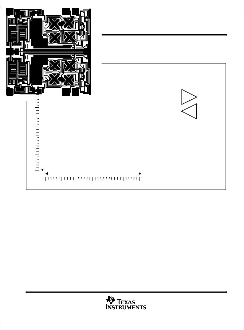
TL082Y chip information
These chips, when properly assembled, display characteristics similar to the TL082. Thermal compression or ultrasonic bonding may be used on the doped-aluminum bonding pads. Chips may be mounted with conductive epoxy or a gold-silicon preform.
|
|
|
|
|
BONDING PAD ASSIGNMENTS |
|
||
|
|
|
|
|
|
|
|
|
|
|
|
|
(7) |
(6) |
(5) |
||
|
|
|
|
|
|
|
||
61 |
(8) |
|
|
|
(4) |
|||
|
|
|
|
(1) |
(2) |
(3) |
||
|
|
|
|
|
|
|
|
|
|
|
|
|
|
|
|
|
|
|
|
|
|
|
|
61 |
|
|
|
|
|
|
VCC+ |
|
|
|
||
|
(3) |
|
|
|
(8) |
|
|
|
|
1IN + |
+ |
|
|
|
|
|
|||
|
|
|
|
(1) |
1OUT |
||||
|
|
||||||||
|
|
|
|
||||||
|
|
|
|
|
|
|
|||
1IN ± |
(2) |
± |
|
|
|
|
|||
|
|
|
|||||||
|
|
|
|
|
|||||
|
|
|
|
(5) |
|
||||
|
|
|
|||||||
|
|
|
+ |
2IN + |
|||||
2OUT |
(7) |
|
|
||||||
|
|
||||||||
|
|
|
|
|
|
||||
|
|
|
|
|
± |
(6) |
2IN ± |
||
|
|
|
|
|
|||||
|
|
|
|
|
|
||||
|
|
|
|
|
|
|
|||
|
|
|
|
|
|||||
|
|
|
|
|
(4) |
|
|
|
|
|
|
|
|
VCC ± |
|
|
|
||
CHIP THICKNESS: 15 TYPICAL
BONDING PADS: 4 × 4 MINIMUM
TJmax = 150°C
TOLERANCES ARE ± 10%.
ALL DIMENSIONS ARE IN MILS.
PIN (4) IS INTERNALLY CONNECTED TO BACKSIDE OF CHIP.
POST OFFICE BOX 655303 •DALLAS, TEXAS 75265 |
5 |

TL081, TL081A, TL081B, TL082, TL082A, TL082B
TL082Y, TL084, TL084A, TL084B, TL084Y
JFET-INPUT OPERATIONAL AMPLIFIERS
SLOS081E ± FEBRUARY 1977 ± REVISED FEBRUARY 1999
TL084Y chip information
These chips, when properly assembled, display characteristics similar to the TL084. Thermal compression or ultrasonic bonding may be used on the doped-aluminum bonding pads. Chips may be mounted with conductive epoxy or a gold-silicon preform.
BONDING PAD ASSIGNMENTS
|
|
|
|
(13) |
(12) |
(11) |
(10) |
(9) |
|
|
|
|
(14) |
|
|
|
(8) |
62 |
(1) |
|
|
|
(7) |
|||
|
|
|
|
|
|
|
||
|
|
|
|
(2) |
(3) |
(4) |
|
(6) |
|
|
|
|
|
|
|
|
|
|
|
|
|
|
|
|
|
|
|
|
|
|
|
|
105 |
|
|
|
|
|
|
VCC+ |
|
|
|
|
|
(3) |
|
|
(4) |
|
|
|
|
1IN + |
+ |
|
|
|
|
|||
|
|
|
(1) |
|
1OUT |
|||
|
|
|
|
|
|
|
||
1IN ± |
(2) |
± |
|
|
|
|||
|
|
|||||||
|
|
|
|
|||||
|
|
|
(5) |
|
|
|||
|
|
|
|
|||||
|
|
|
+ |
|
2IN + |
|||
2OUT |
(7) |
|
|
|||||
|
|
|||||||
|
|
|
|
|
||||
|
|
|
|
|
(6) |
|
|
|
|
|
± |
|
2IN ± |
||||
|
|
|
|
|||||
3IN + |
(10) |
|
|
|||||
|
|
|||||||
+ |
|
|
|
|
||||
|
|
|
(8) |
|
3OUT |
|||
|
|
|
|
|||||
|
|
|
|
|
|
|
||
3IN ± |
(9) |
± |
|
|
|
|||
|
|
|
||||||
|
|
|
|
|||||
|
|
|
|
|
|
|||
|
|
|
|
|
|
|||
(14)+ (12) 4IN +
4OUT |
(13) 4IN ± |
± |
(11) VCC ±
CHIP THICKNESS: 15 TYPICAL BONDING PADS: 4 × 4 MINIMUM TJmax = 150°C
TOLERANCES ARE ± 10%.
ALL DIMENSIONS ARE IN MILS.
PIN (11) IS INTERNALLY CONNECTED TO BACKSIDE OF CHIP.
6 |
POST OFFICE BOX 655303 •DALLAS, TEXAS 75265 |

TL081, TL081A, TL081B, TL082, TL082A, TL082B
TL082Y, TL084, TL084A, TL084B, TL084Y
JFET-INPUT OPERATIONAL AMPLIFIERS
SLOS081E ± FEBRUARY 1977 ± REVISED FEBRUARY 1999
absolute maximum ratings over operating free-air temperature range (unless otherwise noted)²
|
|
TL08_C |
|
|
|
|
|
|
TL08_AC |
TL08_I |
TL084Q |
TL08_M |
UNIT |
|
|
TL08_BC |
|
|
|
|
|
|
|
|
|
|
|
Supply voltage, VCC + (see Note 1) |
|
18 |
18 |
18 |
18 |
V |
Supply voltage VCC ± (see Note 1) |
|
± 18 |
± 18 |
± 18 |
± 18 |
V |
Differential input voltage, VID (see Note 2) |
|
± 30 |
± 30 |
± 30 |
± 30 |
V |
Input voltage, VI (see Notes 1 and 3) |
|
± 15 |
± 15 |
± 15 |
± 15 |
V |
Duration of output short circuit (see Note 4) |
|
unlimited |
unlimited |
unlimited |
unlimited |
|
|
|
|
|
|
|
|
Continuous total power dissipation |
|
|
See Dissipation Rating Table |
|
||
|
|
|
|
|
|
|
Operating free-air temperature range, TA |
|
0 to 70 |
± 40 to 85 |
± 40 to 125 |
± 55 to 125 |
°C |
Storage temperature range, Tstg |
|
± 65 to 150 |
± 65 to 150 |
± 65 to 150 |
± 65 to 150 |
°C |
Case temperature for 60 seconds, TC |
FK package |
|
|
|
260 |
°C |
Lead temperature 1,6 mm (1/16 inch) from case for 60 |
J or JG package |
|
|
|
300 |
°C |
seconds |
|
|
|
|||
|
|
|
|
|
|
|
|
|
|
|
|
|
|
Lead temperature 1,6 mm (1/16 inch) from case for 10 |
D, N, P, or |
260 |
260 |
260 |
|
°C |
seconds |
PW package |
|
||||
|
|
|
|
|
||
|
|
|
|
|
|
|
² Stresses beyond those listed under ªabsolute maximum ratingsº may cause permanent damage to the device. These are stress ratings only, and functional operation of the device at these or any other conditions beyond those indicated under ªrecommended operating conditionsº is not implied. Exposure to absolute-maximum-rated conditions for extended periods may affect device reliability.
NOTES: 1. All voltage values, except differential voltages, are with respect to the midpoint between VCC + and VCC ±.
2.Differential voltages are at IN+ with respect to IN ±.
3.The magnitude of the input voltage must never exceed the magnitude of the supply voltage or 15 V, whichever is less.
4.The output may be shorted to ground or to either supply. Temperature and/or supply voltages must be limited to ensure that the dissipation rating is not exceeded.
DISSIPATION RATING TABLE
PACKAGE |
TA ≤ 25°C |
DERATING |
DERATE |
TA = 70°C |
TA = 85°C |
TA = 125°C |
|
POWER RATING |
FACTOR |
ABOVE TA |
POWER RATING |
POWER RATING |
POWER RATING |
||
|
|||||||
D (8 pin) |
680 mW |
5.8 mW/°C |
32°C |
460 mW |
373 mW |
N/A |
|
D (14 pin) |
680 mW |
7.6 mW/°C |
60°C |
604 mW |
490 mW |
186 mW |
|
FK |
680 mW |
11.0 mW/°C |
88°C |
680 mW |
680 mW |
273 mW |
|
J |
680 mW |
11.0 mW/°C |
88°C |
680 mW |
680 mW |
273 mW |
|
JG |
680 mW |
8.4 mW/°C |
69°C |
672 mW |
546 mW |
210 mW |
|
N |
680 mW |
9.2 mW/°C |
76°C |
680 mW |
597 mW |
N/A |
|
P |
680 mW |
8.0 mW/°C |
65°C |
640 mW |
520 mW |
N/A |
|
PW (8 pin) |
525 mW |
4.2 mW/°C |
25°C |
336 mW |
N/A |
N/A |
|
PW (14 pin) |
700 mW |
5.6 mW/°C |
25°C |
448 mW |
N/A |
N/A |
|
U |
675 mW |
5.4 mW/°C |
25°C |
432 mW |
351 mW |
135 mW |
|
W |
680 mW |
8.0 mW/°C |
65°C |
640 mW |
520 mW |
200 mW |
|
|
|
|
|
|
|
|
POST OFFICE BOX 655303 •DALLAS, TEXAS 75265 |
7 |
8
75265 TEXAS DALLAS, •655303 BOX OFFICE POST
electrical characteristics, VCC± = ±15 V (unless otherwise noted)
|
|
|
|
|
|
TL081C |
|
|
TL081AC |
|
|
TLO81BC |
|
|
TL081I |
|
|
|
PARAMETER |
TEST CONDITIONS |
T ² |
|
TL082C |
|
|
TL082AC |
|
|
TL082BC |
|
|
TL082I |
|
UNIT |
|
|
|
TL084C |
|
|
TL084AC |
|
|
TL084BC |
|
|
TL084I |
|
|||||
|
|
|
|
A |
|
|
|
|
|
|
|
|
|
||||
|
|
|
|
|
MIN |
TYP |
MAX |
MIN |
TYP |
MAX |
MIN |
TYP |
MAX |
MIN |
TYP |
MAX |
|
VIO |
Input offset voltage |
VO = 0 |
RS = 50 Ω |
25°C |
|
3 |
15 |
|
3 |
6 |
|
2 |
3 |
|
3 |
6 |
mV |
|
|
|
|
|
|
|
|
|
|
|
|
|
|||||
Full range |
|
|
20 |
|
|
7.5 |
|
|
5 |
|
|
9 |
|||||
|
|
|
|
|
|
|
|
|
|
|
|
|
|||||
|
Temperature |
|
|
|
|
|
|
|
|
|
|
|
|
|
|
|
|
α VIO |
coefficient of input |
VO = 0 |
RS = 50 Ω |
Full range |
|
18 |
|
|
18 |
|
|
18 |
|
|
18 |
|
μV/°C |
|
offset voltage |
|
|
|
|
|
|
|
|
|
|
|
|
|
|
|
|
IIO |
Input offset current ³ |
VO = 0 |
|
25°C |
|
5 |
200 |
|
5 |
100 |
|
5 |
100 |
|
5 |
100 |
pA |
|
|
|
|
|
|
|
|
|
|
|
|
|
|
|
|||
|
Full range |
|
|
2 |
|
|
2 |
|
|
2 |
|
|
10 |
nA |
|||
|
|
|
|
|
|
|
|
|
|
|
|
|
|
|
|
|
|
IIB |
Input bias current ³ |
VO = 0 |
|
25°C |
|
30 |
400 |
|
30 |
200 |
|
30 |
200 |
|
30 |
200 |
pA |
|
|
|
|
|
|
|
|
|
|
|
|
|
|
|
|||
|
Full range |
|
|
10 |
|
|
7 |
|
|
7 |
|
|
20 |
nA |
|||
|
|
|
|
|
|
|
|
|
|
|
|
|
|
|
|
|
|
|
Common-mode input |
|
|
|
|
± 12 |
|
|
± 12 |
|
|
± 12 |
|
|
± 12 |
|
|
VICR |
|
|
25°C |
± 11 |
to |
|
± 11 |
to |
|
± 11 |
to |
|
± 11 |
to |
|
V |
|
voltage range |
|
|
|
|
|
|
|||||||||||
|
|
|
|
|
15 |
|
|
15 |
|
|
15 |
|
|
15 |
|
|
|
|
|
|
|
|
|
|
|
|
|
|
|
|
|
||||
|
|
|
|
|
|
|
|
|
|
|
|
|
|
|
|
|
|
|
Maximum peak |
RL = 10 kΩ |
|
25°C |
± 12 |
± 13.5 |
|
± 12 |
± 13.5 |
|
± 12 |
± 13.5 |
|
± 12 |
± 13.5 |
|
|
VOM |
RL ≥ 10 kΩ |
|
|
± 12 |
|
|
± 12 |
|
|
± 12 |
|
|
± 12 |
|
|
V |
|
output voltage swing |
|
Full range |
|
|
|
|
|
|
|
|
|||||||
|
RL ≥ 2 kΩ |
|
± 10 |
± 12 |
|
± 10 |
± 12 |
|
± 10 |
± 12 |
|
± 10 |
± 12 |
|
|
||
|
|
|
|
|
|
|
|
|
|||||||||
AVD |
Large-signal |
VO = ± 10 V, |
RL ≥ 2 kΩ |
25°C |
25 |
200 |
|
50 |
200 |
|
50 |
200 |
|
50 |
200 |
|
V/mV |
differential voltage |
|
|
|
|
|
|
|
|
|
|
|
|
|
|
|
||
VO = ± 10 V, |
RL ≥ 2 kΩ |
Full range |
15 |
|
|
25 |
|
|
25 |
|
|
25 |
|
|
|||
|
amplification |
|
|
|
|
|
|
|
|
|
|||||||
B1 |
Unity-gain bandwidth |
|
|
25°C |
|
3 |
|
|
3 |
|
|
3 |
|
|
3 |
|
MHz |
ri |
Input resistance |
|
|
25°C |
|
1012 |
|
|
1012 |
|
|
1012 |
|
|
1012 |
|
Ω |
CMRR |
Common-mode |
VIC = VICRmin, |
25°C |
70 |
86 |
|
75 |
86 |
|
75 |
86 |
|
75 |
86 |
|
dB |
|
rejection ratio |
VO = 0, |
RS = 50 Ω |
|
|
|
|
|||||||||||
|
|
|
|
|
|
|
|
|
|
|
|
|
|
|
|||
|
Supply voltage |
VCC = ± 15 V to ± 9 V, |
|
|
|
|
|
|
|
|
|
|
|
|
|
|
|
kSVR |
rejection ratio |
25°C |
70 |
86 |
|
80 |
86 |
|
80 |
86 |
|
80 |
86 |
|
dB |
||
VO = 0, |
RS = 50 Ω |
|
|
|
|
||||||||||||
|
( VCC± / VIO) |
|
|
|
|
|
|
|
|
|
|
|
|
|
|
|
|
ICC |
Supply current |
VO = 0, |
No load |
25°C |
|
1.4 |
2.8 |
|
1.4 |
2.8 |
|
1.4 |
2.8 |
|
1.4 |
2.8 |
mA |
(per amplifier) |
|
|
|
|
|||||||||||||
|
|
|
|
|
|
|
|
|
|
|
|
|
|
|
|
|
|
|
|
|
|
|
|
|
|
|
|
|
|
|
|
|
|
|
|
VO1/ VO2 |
Crosstalk attenuation |
AVD = 100 |
|
25°C |
|
120 |
|
|
120 |
|
|
120 |
|
|
120 |
|
dB |
²All characteristics are measured under open-loop conditions with zero common-mode voltage unless otherwise specified. Full range for TA is 0°C to 70°C for TL08_C, TL08_AC, TL08_BC and ± 40°C to 85°C for TL08_I.
³Input bias currents of a FET-input operational amplifier are normal junction reverse currents, which are temperature sensitive as shown in Figure 17. Pulse techniques must be used that maintain the junction temperature as close to the ambient temperature as possible.
TL082B TL082A, TL082, TL081B, TL081A, TL081, TL084Y TL084B, TL084A, TL084, TL082Y, AMPLIFIERS OPERATIONAL INPUT-JFET 1999 FEBRUARY REVISED ± 1977 FEBRUARY ± SLOS081E |
7±11±94 Date: Release Template |
TL081, TL081A, TL081B, TL082, TL082A, TL082B
TL082Y, TL084, TL084A, TL084B, TL084Y
JFET-INPUT OPERATIONAL AMPLIFIERS
SLOS081E ± FEBRUARY 1977 ± REVISED FEBRUARY 1999
electrical characteristics, VCC ± = ± 15 V (unless otherwise noted)
|
PARAMETER |
|
TEST CONDITIONS² |
T |
TL081M, TL082M |
TL084Q, TL084M |
UNIT |
||||||
|
|
|
|
|
|
|
|
||||||
|
|
|
|
|
|
|
|
||||||
|
|
|
|
|
|
A |
MIN |
TYP |
MAX |
MIN |
TYP |
MAX |
|
|
|
|
|
|
|
|
|
||||||
VIO |
Input offset voltage |
VO = 0, |
RS = 50 Ω |
25°C |
|
3 |
6 |
|
3 |
9 |
mV |
||
|
|
|
|
|
|
|
|||||||
Full range |
|
|
9 |
|
|
15 |
|||||||
|
|
|
|
|
|
|
|
|
|
|
|||
|
|
|
|
|
|
|
|
|
|
|
|
|
|
|
Temperature |
|
|
|
|
|
|
|
|
|
|
|
|
αVIO |
coefficient of input |
VO = 0 |
RS = 50 Ω |
Full range |
|
18 |
|
|
18 |
|
μV/°C |
||
|
offset voltage |
|
|
|
|
|
|
|
|
|
|
|
|
|
|
|
|
|
|
|
|
|
|
|
|
|
|
I |
Input offset current³ |
V |
O |
= 0 |
|
25°C |
|
5 |
100 |
|
5 |
100 |
pA |
|
|
|
|
|
|
|
|
|
|||||
|
|
|
|
|
|
|
|
|
|||||
IO |
|
|
|
|
125°C |
|
|
20 |
|
|
20 |
nA |
|
|
|
|
|
|
|
|
|
|
|
||||
I |
Input bias current³ |
V |
O |
= 0 |
|
25°C |
|
30 |
200 |
|
30 |
200 |
pA |
|
|
|
|
|
|
|
|
|
|||||
|
|
|
|
|
|
|
|
|
|||||
IB |
|
|
|
|
125°C |
|
|
50 |
|
|
50 |
nA |
|
|
|
|
|
|
|
|
|
|
|
||||
|
Common-mode input |
|
|
|
|
|
|
± 12 |
|
|
± 12 |
|
|
VICR |
|
|
|
|
25°C |
± 11 |
to |
|
± 11 |
to |
|
V |
|
voltage range |
|
|
|
|
|
|
|||||||
|
|
|
|
|
|
|
15 |
|
|
15 |
|
|
|
|
|
|
|
|
|
|
|
|
|
|
|
||
|
|
|
|
|
|
|
|
|
|
|
|
||
|
Maximum peak |
RL = 10 kΩ |
|
25°C |
± 12 |
± 13.5 |
|
± 12 |
± 13.5 |
|
|
||
VOM |
RL ≥ 10 kΩ |
|
|
± 12 |
|
|
± 12 |
|
|
V |
|||
output voltage swing |
|
Full range |
|
|
|
|
|||||||
|
RL ≥ 2 kΩ |
|
± 10 |
± 12 |
|
± 10 |
± 12 |
|
|
||||
|
|
|
|
|
|
|
|||||||
AVD |
Large-signal |
VO = ± 10 V, |
RL ≥ 2 kΩ |
25°C |
25 |
200 |
|
25 |
200 |
|
V/mV |
||
differential voltage |
|
|
|
|
|
|
|
|
|
|
|
||
VO = ± 10 V, |
RL ≥ 2 kΩ |
Full range |
15 |
|
|
15 |
|
|
|||||
|
amplification |
|
|
|
|
|
|||||||
B1 |
Unity-gain bandwidth |
|
|
|
|
25°C |
|
3 |
|
|
3 |
|
MHz |
ri |
Input resistance |
|
|
|
|
25°C |
|
1012 |
|
|
1012 |
|
Ω |
CMRR |
Common-mode |
VIC = VICRmin, |
25°C |
80 |
86 |
|
80 |
86 |
|
dB |
|||
rejection ratio |
VO = 0, |
RS = 50 Ω |
|
|
|||||||||
|
|
|
|
|
|
|
|
|
|||||
|
Supply voltage |
VCC = ± 15 V to ± 9 V, |
|
|
|
|
|
|
|
|
|||
kSVR |
rejection ratio |
25°C |
80 |
86 |
|
80 |
86 |
|
dB |
||||
VO = 0, |
RS = 50 Ω |
|
|
||||||||||
|
( VCC ± / VIO) |
|
|
|
|
|
|
|
|
||||
|
|
|
|
|
|
|
|
|
|
|
|
|
|
ICC |
Supply current |
VO = 0, |
No load |
25°C |
|
1.4 |
2.8 |
|
1.4 |
2.8 |
mA |
||
(per amplifier) |
|
|
|||||||||||
|
|
|
|
|
|
|
|
|
|
|
|
|
|
|
|
|
|
|
|
|
|
|
|
|
|
||
VO1/ VO2 |
Crosstalk attenuation |
AVD = 100 |
|
25°C |
|
120 |
|
|
120 |
|
dB |
||
² All characteristics are measured under open-loop conditions with zero common-mode input voltage unless otherwise specified.
³Input bias currents of a FET-input operational amplifier are normal junction reverse currents, which are temperature sensitive as shown in Figure 17. Pulse techniques must be used that maintain the junction temperatures as close to the ambient temperature as is possible.
operating characteristics, VCC ± = ±15 V, TA = 25°C (unless otherwise noted)
|
PARAMETER |
|
TEST CONDITIONS |
|
MIN |
TYP |
MAX |
UNIT |
|||
|
|
|
|
|
|
|
|
|
|
|
|
|
|
VI = 10 V, |
RL = 2 kΩ, |
CL = 100 pF, |
See Figure 1 |
8 |
13 |
|
|
|
|
SR |
Slew rate at unity gain |
VI = 10 V, |
RL = 2 kΩ, |
CL = 100 pF, |
|
|
|
|
V/μs |
||
|
|
TA = ± 55°C to 125°C, |
See Figure 1 |
|
|
5 |
|
|
|
|
|
|
|
|
|
|
|
|
|
|
|
||
tr |
Rise time |
VI = 20 mV, |
RL = 2 kΩ, |
CL = 100 pF, |
See Figure 1 |
|
0.05 |
|
μs |
||
|
Overshoot factor |
|
20% |
|
|
|
|
||||
|
|
|
|
|
|
|
|
|
|
||
|
|
|
|
|
|
|
|
|
|
|
|
Vn |
Equivalent input noise |
RS = 20 Ω |
f = 1 kHz |
|
|
|
18 |
|
nV/√ |
Hz |
|
|
|
|
|
|
|
|
|
|
|||
voltage |
f = 10 Hz to 10 kHz |
|
|
4 |
|
μV |
|||||
|
|
|
|
|
|||||||
|
|
|
|
|
|
|
|
|
|
|
|
|
Equivalent input noise |
|
|
|
|
|
|
|
|
|
|
In |
RS = 20 Ω, |
f = 1 kHz |
|
|
|
0.01 |
|
pA/√ Hz |
|||
current |
|
|
|
|
|||||||
THD |
Total harmonic distortion |
VIrms = 6 V, |
AVD = 1, |
RS ≤ 1 kΩ, |
RL ≥ 2 kΩ, |
|
0.003% |
|
|
|
|
f = 1 kHz |
|
|
|
|
|
|
|
|
|||
|
|
|
|
|
|
|
|
|
|
|
|
|
|
|
|
|
|
|
|
|
|
|
|
On products compliant to MIL-PRF-38535, this parameter is not production tested.
POST OFFICE BOX 655303 •DALLAS, TEXAS 75265 |
9 |
 Loading...