


Texas Instruments TLC271CPWLE, TLC271CPW, TLC271CPSR, TLC271CPS, TLC271CP Datasheet
...DInput Offset Voltage Drift . . . Typically 0.1 µV/Month, Including the First 30 Days
DWide Range of Supply Voltages Over
Specified Temperature Range: 0°C to 70°C . . . 3 V to 16 V ±40°C to 85°C . . . 4 V to 16 V
±55°C to 125°C . . . 5 V to 16 V
DSingle-Supply Operation
DCommon-Mode Input Voltage Range Extends Below the Negative Rail (C-Suffix and I-Suffix Types)
DLow Noise . . . 25 nV/√ Hz Typically at f = 1 kHz (High-Bias Mode)
DOutput Voltage Range includes Negative Rail
DHigh Input Impedance . . . 1012 Ω Typ
DESD-Protection Circuitry
DSmall-Outline Package Option Also Available in Tape and Reel
DDesigned-In Latch-Up Immunity
description
TLC271, TLC271A, TLC271B LinCMOS PROGRAMMABLE LOW-POWER
OPERATIONAL AMPLIFIERS
SLOS090C ± NOVEMBER 1987 ± REVISED AUGUST 1997
D, JG, OR P PACKAGE
(TOP VIEW)
OFFSET N1 |
|
1 |
8 |
|
BIAS SELECT |
|
|
||||
IN ± |
|
2 |
7 |
|
VDD |
|
|
||||
IN + |
|
3 |
6 |
|
OUT |
|
|
||||
GND |
|
4 |
5 |
|
OFFSET N2 |
|
|
||||
|
|
|
|
|
|
|
|
|
|
|
|
FK PACKAGE (TOP VIEW)
|
NC |
OFFSET N1 |
NC |
BIAS SELECT |
NC |
|
NC |
3 |
2 |
1 |
20 19 |
NC |
|
4 |
|
|
|
18 |
||
IN ± |
5 |
|
|
|
17 |
VDD |
NC |
6 |
|
|
|
16 |
NC |
IN + |
7 |
|
|
|
15 |
OUT |
NC |
8 |
|
|
|
14 |
NC |
|
9 |
10 11 12 13 |
|
|||
NC GND NC |
NC |
The TLC271 operational amplifier combines a wide range of input offset voltage grades with low offset voltage drift and high input impedance. In addition, the TLC271 offers a bias-select mode
that allows the user to select the best combination of power dissipation and ac performance for a particular application. These devices use Texas Instruments silicon-gate LinCMOS technology, which provides offset voltage stability far exceeding the stability available with conventional metal-gate processes.
AVAILABLE OPTIONS
|
|
|
PACKAGE |
|
|
|
VIOmax |
|
|
|
|
TA |
SMALL |
CHIP |
CERAMIC |
PLASTIC |
|
AT 25°C |
OUTLINE |
CARRIER |
DIP |
DIP |
|
|
|
(D) |
(FK) |
(JG) |
(P) |
|
|
|
|
|
|
0°C |
2 mV |
TLC271BCD |
|
|
TLC271BCP |
to |
5 mV |
TLC271ACD |
Ð |
Ð |
TLC271ACP |
70°C |
10 mV |
TLC271CD |
|
|
TLC271CP |
|
|
|
|
|
|
± 40°C |
2 mV |
TLC271BID |
|
|
TLC271BIP |
to |
5 mV |
TLC271AID |
Ð |
Ð |
TLC271AIP |
85°C |
10 mV |
TLC271ID |
|
|
TLC271IP |
|
|
|
|
|
|
± 55°C |
|
|
|
|
|
to |
10 mV |
TLC271MD |
TLC271MFK |
TLC271MJG |
TLC271MP |
125°C |
|
|
|
|
|
|
|
|
|
|
|
The D package is available taped and reeled. Add R suffix to the device type (e.g.,
TLC271BCDR).
Please be aware that an important notice concerning availability, standard warranty, and use in critical applications of Texas Instruments semiconductor products and disclaimers thereto appears at the end of this data sheet.
LinCMOS is a trademark of Texas Instruments Incorporated.
PRODUCTION DATA information is current as of publication date. Products conform to specifications per the terms of Texas Instruments standard warranty. Production processing does not necessarily include testing of all parameters.
Copyright 1997, Texas Instruments Incorporated
POST OFFICE BOX 655303 •DALLAS, TEXAS 75265 |
1 |
TLC271, TLC271A, TLC271B
LinCMOS PROGRAMMABLE LOW-POWER
OPERATIONAL AMPLIFIERS
SLOS090C ± NOVEMBER 1987 ± REVISED AUGUST 1997
8DEVICE FEATURES
PARAMETER² |
|
|
BIAS-SELECT MODE |
|
UNIT |
|||||
|
|
|
|
|
|
|||||
|
HIGH |
|
MEDIUM |
|
LOW |
|||||
|
|
|
|
|
|
|
|
|||
|
|
|
|
|
|
|
|
|
|
|
PD |
|
|
3375 |
|
525 |
|
50 |
W |
||
SR |
|
|
3.6 |
|
0.4 |
|
0.03 |
V/ s |
||
|
|
|
|
|
|
|
|
|
||
Vn |
|
|
25 |
|
32 |
|
68 |
nV/√ |
Hz |
|
B1 |
|
|
1.7 |
|
0.5 |
|
0.09 |
MHz |
||
AVD |
|
|
23 |
|
170 |
|
480 |
V/mV |
||
² Typical at V |
DD |
= 5 V, T = 25°C |
|
|
|
|
||||
|
|
A |
|
|
|
|
|
|
|
|
description (continued)
Using the bias-select option, these cost-effective devices can be programmed to span a wide range of applications that previously required BiFET, NFET or bipolar technology. Three offset voltage grades are available (C-suffix and I-suffix types), ranging from the low-cost TLC271 (10 mV) to the TLC271B (2 mV) low-offset version. The extremely high input impedance and low bias currents, in conjunction with good common-mode rejection and supply voltage rejection, make these devices a good choice for new state-of-the-art designs as well as for upgrading existing designs.
In general, many features associated with bipolar technology are available in LinCMOS operational amplifiers, without the power penalties of bipolar technology. General applications such as transducer interfacing, analog calculations, amplifier blocks, active filters, and signal buffering are all easily designed with the TLC271. The devices also exhibit low-voltage single-supply operation, making them ideally suited for remote and inaccessible battery-powered applications. The common-mode input voltage range includes the negative rail.
A wide range of packaging options is available, including small-outline and chip-carrier versions for high-density system applications.
The device inputs and output are designed to withstand ±100-mA surge currents without sustaining latch-up.
The TLC271 incorporates internal ESD-protection circuits that prevent functional failures at voltages up to 2000 V as tested under MIL-STD-883C, Method 3015.2; however, care should be exercised in handling these devices as exposure to ESD may result in the degradation of the device parametric performance.
The C-suffix devices are characterized for operation from 0°C to 70°C. The I-suffix devices are characterized for operation from ± 40°C to 85°C. The M-suffix devices are characterized for operation over the full military temperature range of ± 55°C to 125°C.
bias-select feature
The TLC271 offers a bias-select feature that allows the user to select any one of three bias levels depending on the level of performance desired. The tradeoffs between bias levels involve ac performance and power dissipation (see Table 1).
2 |
POST OFFICE BOX 655303 •DALLAS, TEXAS 75265 |
TLC271, TLC271A, TLC271B
LinCMOS PROGRAMMABLE LOW-POWER
OPERATIONAL AMPLIFIERS
SLOS090C ± NOVEMBER 1987 ± REVISED AUGUST 1997
bias-select feature (continued)
Table 1. Effect of Bias Selection on Performance
|
TYPICAL PARAMETER VALUES |
|
MODE |
|
|
|
|
|
|
|
|
UNIT |
|||
|
HIGH BIAS |
MEDIUM BIAS |
LOW BIAS |
||||
|
TA = 25°C, VDD = 5 V |
||||||
|
|
|
|
||||
|
|
RL = 10 kΩ |
RL = 100 kΩ |
RL = 1 MΩ |
|
|
|
PD |
Power dissipation |
3.4 |
0.5 |
0.05 |
mW |
||
SR |
Slew rate |
3.6 |
0.4 |
0.03 |
V/µs |
||
Vn |
Equivalent input noise voltage at f = 1 kHz |
25 |
32 |
68 |
nV/√ |
|
|
Hz |
|
||||||
B1 |
Unity-gain bandwidth |
1.7 |
0.5 |
0.09 |
MHz |
||
φm |
Phase margin |
46° |
40° |
34° |
|
|
|
AVD |
Large-signal differential voltage amplification |
23 |
170 |
480 |
V/mV |
||
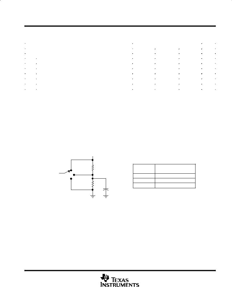
bias selection
Bias selection is achieved by connecting the bias select pin to one of three voltage levels (see Figure 1). For medium-bias applications, it is recommended that the bias select pin be connected to the midpoint between the supply rails. This procedure is simple in split-supply applications, since this point is ground. In single-supply applications, the medium-bias mode necessitates using a voltage divider as indicated in Figure 1. The use of large-value resistors in the voltage divider reduces the current drain of the divider from the supply line. However, large-value resistors used in conjunction with a large-value capacitor require significant time to charge up to the supply midpoint after the supply is switched on. A voltage other than the midpoint can be used if it is within the voltages specified in Figure 1.
bias selection (continued)
|
|
VDD |
|
|
|
|
Low |
1 MΩ |
BIAS MODE |
BIAS-SELECT VOLTAGE |
|
To the Bias |
(single supply) |
||||
Medium |
|
|
|||
|
|
|
|||
Select Pin |
|
Low |
VDD |
||
|
|
||||
|
|
|
|||
|
High |
|
Medium |
1 V to VDD ± 1 V |
|
|
1 MΩ |
|
High |
GND |
|
|
|
|
|||
|
|
|
0.01 µF |
|
Figure 1. Bias Selection for Single-Supply Applications
high-bias mode
In the high-bias mode, the TLC271 series features low offset voltage drift, high input impedance, and low noise. Speed in this mode approaches that of BiFET devices but at only a fraction of the power dissipation. Unity-gain bandwidth is typically greater than 1 MHz.
medium-bias mode
The TLC271 in the medium-bias mode features low offset voltage drift, high input impedance, and low noise. Speed in this mode is similar to general-purpose bipolar devices but power dissipation is only a fraction of that consumed by bipolar devices.
POST OFFICE BOX 655303 •DALLAS, TEXAS 75265 |
3 |

TLC271, TLC271A, TLC271B
LinCMOS PROGRAMMABLE LOW-POWER
OPERATIONAL AMPLIFIERS
SLOS090C ± NOVEMBER 1987 ± REVISED AUGUST 1997
low-bias mode
In the low-bias mode, the TLC271 features low offset voltage drift, high input impedance, extremely low power consumption, and high differential voltage gain.
ORDER OF CONTENTS
TOPIC |
BIAS MODE |
|
|
|
|
schematic |
all |
|
|
|
|
absolute maximum ratings |
all |
|
|
|
|
recommended operating conditions |
all |
|
|
|
|
electrical characteristics |
high |
|
operating characteristics |
||
(Figures 2 ± 33) |
||
typical characteristics |
||
|
||
|
|
|
electrical characteristics |
medium |
|
operating characteristics |
||
(Figures 34 ± 65) |
||
typical characteristics |
||
|
||
|
|
|
electrical characteristics |
low |
|
operating characteristics |
||
(Figures 66 ± 97) |
||
typical characteristics |
||
|
||
|
|
|
parameter measurement information |
all |
|
|
|
|
application information |
all |
|
|
|
equivalent schematic
VDD
P3 |
P12 |
|
P9A |
|
R6 |
|
|
|
P4 |
|
P5 |
P9B |
P11 |
|
|
|
|
|
|
||
P1 |
|
P2 |
R2 |
|
|
|
|
IN ± |
|
|
|
|
|
|
|
R1 |
|
|
|
|
|
|
P10 |
|
|
|
|
N5 |
|
|
|
|
|
|
|
|
|
N11 |
|
|
|
|
|
|
|
|
|
IN + |
|
|
R5 |
C1 |
P6A |
P6B P7B |
P7A P8 |
|
|
|
|
|
|
|
|
|
|
|
N3 |
|
|
|
N12 |
|
|
|
|
|
|
N9 |
|
|
|
|
|
|
|
|
|
|
|
|
|
|
|
N6 |
|
|
N1 |
N2 |
|
|
|
|
N7 |
|
|
|
|
|
|
||
|
D1 |
|
D2 |
N4 |
|
|
N13 |
R3 |
|
|
|
R7 |
|||
|
|
|
|
|
|
||
|
|
R4 |
|
|
|
|
N10 |
|
|
|
|
|
|
|
|
|
OFFSET |
OFFSET |
|
|
OUT |
GND |
BIAS |
|
N1 |
N2 |
|
|
|
|
SELECT |
4 |
POST OFFICE BOX 655303 •DALLAS, TEXAS 75265 |

TLC271, TLC271A, TLC271B
LinCMOS PROGRAMMABLE LOW-POWER
OPERATIONAL AMPLIFIERS
SLOS090C ± NOVEMBER 1987 ± REVISED AUGUST 1997
absolute maximum ratings over operating free-air temperature (unless otherwise noted)²
Supply voltage, VDD (see Note 1) . . . . . . . . . . . . . . . . . . . . . . . . . . . . . . . . . . . . . . . |
. . . . . . . . . . . |
. . . . . . . . . . 18 V |
Differential input voltage, VID (see Note 2) . . . . . . . . . . . . . . . . . . . . . . . . . . . . . . . |
. . . . . . . . . . . . |
. . . . . . . . ± VDD |
Input voltage range, VI (any input) . . . . . . . . . . . . . . . . . . . . . . . . . . . . . . . . . . . . . . . |
. . . . . . . . . . . . |
± 0.3 V to VDD |
Input current, II . . . . . . . . . . . . . . . . . . . . . . . . . . . . . . . . . . . . . . . . . . . . . . . . . . . . . . . |
. . . . . . . . . . . . |
. . . . . . . ± 5 mA |
Output current, IO . . . . . . . . . . . . . . . . . . . . . . . . . . . . . . . . . . . . . . . . . . . . . . . . . . . . . |
. . . . . . . . . . . . |
. . . . . . ± 30 mA |
Duration of short-circuit current at (or below) 25°C (see Note 3) . . . . . . . . . . . . . |
. . . . . . . . . . . . |
. . . . . Unlimited |
Continuous total dissipation . . . . . . . . . . . . . . . . . . . . . . . . . . . . . . . . . . . . . . . . . . . |
See Dissipation Rating Table |
|
Operating free-air temperature, TA: C suffix . . . . . . . . . . . . . . . . . . . . . . . . . . . . . . |
. . . . . . . . . . . . |
. . 0°C to 70°C |
I suffix . . . . . . . . . . . . . . . . . . . . . . . . . . . . . . . |
. . . . . . . . . . . . |
± 40°C to 85°C |
M suffix . . . . . . . . . . . . . . . . . . . . . . . . . . . . . . |
. . . . . . . . . . . |
± 55°C to 125°C |
Storage temperature range . . . . . . . . . . . . . . . . . . . . . . . . . . . . . . . . . . . . . . . . . . . . . |
. . . . . . . . . . . |
± 65°C to 150°C |
Case temperature for 60 seconds: FK package . . . . . . . . . . . . . . . . . . . . . . . . . . . |
. . . . . . . . . . . . |
. . . . . . . 260°C |
Lead temperature 1,6 mm (1/16 inch) from case for 10 seconds: D or P package . . . . . . . . . . |
. . . . . . . 260°C |
|
Lead temperature 1,6 mm (1/16 inch) from case for 60 seconds: JG package . |
. . . . . . . . . . . . |
. . . . . . . 300°C |
²Stresses beyond those listed under ªabsolute maximum ratingsº may cause permanent damage to the device. These are stress ratings only, and functional operation of the device at these or any other conditions beyond those indicated under ªrecommended operating conditionsº is not implied. Exposure to absolute-maximum-rated conditions for extended periods may affect device reliability.
NOTES: 1. All voltage values, except differential voltages, are with respect to network ground.
2.Differential voltages are at IN+ with respect to IN ±.
3.The output may be shorted to either supply. Temperature and/or supply voltages must be limited to ensure that the maximum dissipation rating is not exceeded (see application section).
DISSIPATION RATING TABLE
PACKAGE |
TA ≤ 25°C |
DERATING FACTOR |
TA = 70°C |
TA = 85°C |
TA = 125°C |
|
POWER RATING |
ABOVE TA = 25°C |
POWER RATING |
POWER RATING |
POWER RATING |
||
|
||||||
D |
725 mW |
5.8 mW/°C |
464 mW |
377 mW |
145 mW |
|
FK |
1375 mW |
11.0 mW/°C |
880 mW |
715 mW |
275 mW |
|
JG |
1050 mW |
8.4 mW/°C |
672 mW |
546 mW |
210 mW |
|
P |
1000 mW |
8.0 mW/°C |
640 mW |
520 mW |
200 mW |
|
|
|
|
|
|
|
recommended operating conditions
|
|
C SUFFIX |
I SUFFIX |
M SUFFIX |
UNIT |
||||
|
|
|
|
|
|
|
|
||
|
|
MIN |
MAX |
MIN |
MAX |
MIN |
MAX |
||
|
|
|
|||||||
|
|
|
|
|
|
|
|
|
|
Supply voltage, VDD |
|
3 |
16 |
4 |
16 |
5 |
16 |
V |
|
Common-mode input voltage, VIC |
VDD = 5 V |
± 0.2 |
3.5 |
± 0.2 |
3.5 |
0 |
3.5 |
V |
|
VDD = 10 V |
± 0.2 |
8.5 |
± 0.2 |
8.5 |
0 |
8.5 |
|||
|
|
||||||||
Operating free-air temperature, TA |
|
0 |
70 |
± 40 |
85 |
± 55 |
125 |
°C |
|
POST OFFICE BOX 655303 •DALLAS, TEXAS 75265 |
5 |

TLC271, TLC271A, TLC271B
LinCMOS PROGRAMMABLE LOW-POWER
OPERATIONAL AMPLIFIERS
SLOS090C ± NOVEMBER 1987 ± REVISED AUGUST 1997
HIGH-BIAS MODE
electrical characteristics at specified free-air temperature (unless otherwise noted)
|
|
|
TEST |
|
TLC271C, TLC271AC, TLC271BC |
|
|
||||||
|
|
|
T ² |
|
|
|
|
|
|
|
|
|
|
|
PARAMETER |
V |
DD |
= 5 V |
|
V |
DD |
= 10 V |
|
UNIT |
|||
|
|
|
|
||||||||||
|
|
|
CONDITIONS |
A |
|
|
|
|
|
|
|
||
|
|
|
|
|
MIN |
TYP |
MAX |
MIN |
|
TYP |
MAX |
|
|
|
|
|
|
|
|
|
|
|
|
|
|
|
|
|
|
TLC271C |
|
25°C |
|
|
1.1 |
10 |
|
|
1.1 |
10 |
|
|
|
VO = 1.4 V, |
Full range |
|
|
|
12 |
|
|
|
12 |
|
|
|
|
|
|
|
|
|
|
|
|
||||
|
|
|
|
|
|
|
|
|
|
|
|
|
|
|
|
|
25°C |
|
|
0.9 |
5 |
|
|
0.9 |
5 |
|
|
VIO |
Input offset voltage |
TLC271AC |
VIC = 0 V, |
|
|
|
|
mV |
|||||
RS = 50 Ω, |
Full range |
|
|
|
6.5 |
|
|
|
6.5 |
||||
|
|
|
RL = 10 kΩ |
|
|
|
|
|
|
|
|
|
|
|
|
TLC271BC |
25°C |
|
0.34 |
2 |
|
|
0.39 |
2 |
|
||
|
|
|
Full range |
|
|
|
3 |
|
|
|
3 |
|
|
|
|
|
|
|
|
|
|
|
|
|
|||
|
|
|
|
|
|
|
|
|
|
|
|
|
|
αVIO |
Average temperature coefficient |
|
25°C to |
|
|
1.8 |
|
|
|
2 |
|
µV/°C |
|
of input offset voltage |
|
70°C |
|
|
|
|
|
|
|||||
IIO |
Input offset current (see Note 4) |
VO = VDD /2, |
25°C |
|
|
0.1 |
|
|
|
0.1 |
|
pA |
|
VIC = VDD /2 |
70°C |
|
|
7 |
300 |
|
|
7 |
300 |
||||
|
|
|
|
|
|
|
|
||||||
IIB |
Input bias current (see Note 4) |
VO = VDD /2, |
25°C |
|
|
0.6 |
|
|
|
0.7 |
|
pA |
|
VIC = VDD /2 |
70°C |
|
|
40 |
600 |
|
|
50 |
600 |
||||
|
|
|
|
|
|
|
|
||||||
|
|
|
|
|
± 0.2 |
± 0.3 |
|
± 0.2 |
± 0.3 |
|
|
||
|
|
|
|
25°C |
to |
|
to |
|
to |
|
to |
|
V |
|
Common-mode input voltage |
|
|
4 |
|
4.2 |
|
9 |
|
9.2 |
|
|
|
VICR |
|
|
|
|
|
|
|
|
|
|
|
||
|
|
± 0.2 |
|
|
|
± 0.2 |
|
|
|
|
|||
range (see Note 5) |
|
|
|
|
|
|
|
|
|
||||
|
|
Full range |
to |
|
|
|
to |
|
|
|
V |
||
|
|
|
|
|
|
|
|
|
|
||||
|
|
|
|
|
3.5 |
|
|
|
8.5 |
|
|
|
|
|
|
|
|
|
|
|
|
|
|
|
|
|
|
|
|
|
VID = 100 mV, |
25°C |
3.2 |
|
3.8 |
|
8 |
|
8.5 |
|
|
VOH |
High-level output voltage |
0°C |
3 |
|
3.8 |
|
7.8 |
|
8.5 |
|
V |
||
RL = 10 kΩ |
|
|
|
|
|||||||||
|
|
|
70°C |
3 |
|
3.8 |
|
7.8 |
|
8.4 |
|
|
|
|
|
|
|
|
|
|
|
|
|||||
|
|
|
VID = ±100 mV, |
25°C |
|
|
0 |
50 |
|
|
0 |
50 |
|
|
|
|
|
|
|
|
|
|
|
|
|
|
|
VOL |
Low-level output voltage |
0°C |
|
|
0 |
50 |
|
|
0 |
50 |
mV |
||
IOL = 0 |
|
|
|
|
|||||||||
|
|
|
70°C |
|
|
0 |
50 |
|
|
0 |
50 |
|
|
|
|
|
|
|
|
|
|
|
|||||
|
|
|
|
|
|
|
|
|
|
|
|
|
|
|
Large-signal differential |
RL = 10 kΩ, |
25°C |
5 |
|
23 |
|
10 |
|
36 |
|
|
|
|
|
|
|
|
|
|
|
|
|
|
|||
AVD |
0°C |
4 |
|
27 |
|
7.5 |
|
42 |
|
V/mV |
|||
voltage amplification |
See Note 6 |
|
|
|
|
||||||||
|
70°C |
4 |
|
20 |
|
7.5 |
|
32 |
|
|
|||
|
|
|
|
|
|
|
|
|
|||||
|
|
|
|
|
|
|
|
|
|
|
|
|
|
|
|
|
|
25°C |
65 |
|
80 |
|
65 |
|
85 |
|
|
CMRR |
Common-mode rejection ratio |
VIC = VICRmin |
0°C |
60 |
|
84 |
|
60 |
|
88 |
|
dB |
|
|
|
|
|
70°C |
60 |
|
85 |
|
60 |
|
88 |
|
|
|
Supply-voltage rejection ratio |
VDD = 5 V to 10 V |
25°C |
65 |
|
95 |
|
65 |
|
95 |
|
|
|
|
|
|
|
|
|
|
|
|
|
|
|||
kSVR |
0°C |
60 |
|
94 |
|
60 |
|
94 |
|
dB |
|||
( VDD / VIO) |
VO = 1.4 V |
|
|
|
|
||||||||
|
70°C |
60 |
|
96 |
|
60 |
|
96 |
|
|
|||
|
|
|
|
|
|
|
|
|
|||||
|
|
|
|
|
|
|
|
|
|
|
|||
II(SEL) |
Input current (BIAS SELECT) |
VI(SEL) = 0 |
25°C |
|
± 1.4 |
|
|
± 1.9 |
|
µA |
|||
|
|
|
VO = VDD /2, |
25°C |
|
|
675 |
1600 |
|
|
950 |
2000 |
|
IDD |
Supply current |
VIC = VDD /2, |
0°C |
|
|
775 |
1800 |
|
1125 |
2200 |
µA |
||
|
|
|
No load |
70°C |
|
|
575 |
1300 |
|
|
750 |
1700 |
|
|
|
|
|
|
|
|
|
|
|||||
|
|
|
|
|
|
|
|
|
|
|
|
|
|
² Full range is 0°C to 70°C.
NOTES: 4. The typical values of input bias current and input offset current below 5 pA were determined mathematically.
5.This range also applies to each input individually.
6.At VDD = 5 V, VO = 0.25 V to 2 V; at VDD = 10 V, VO = 1 V to 6 V.
6 |
POST OFFICE BOX 655303 •DALLAS, TEXAS 75265 |
TLC271, TLC271A, TLC271B
LinCMOS PROGRAMMABLE LOW-POWER
OPERATIONAL AMPLIFIERS
SLOS090C ± NOVEMBER 1987 ± REVISED AUGUST 1997
HIGH-BIAS MODE
electrical characteristics at specified free-air temperature (unless otherwise noted)
|
|
|
TEST |
|
|
TLC271I, TLC271AI, TLC271BI |
|
|
|||||
|
|
|
T ² |
|
|
|
|
|
|
|
|
|
|
|
PARAMETER |
V |
DD |
= 5 V |
|
V |
DD |
= 10 V |
|
UNIT |
|||
|
|
|
|
||||||||||
|
|
|
CONDITIONS |
A |
|
|
|
|
|
|
|
||
|
|
|
|
|
MIN |
TYP |
MAX |
MIN |
|
TYP |
MAX |
|
|
|
|
|
|
|
|
|
|
|
|
|
|
|
|
|
|
TLC271I |
|
25°C |
|
|
1.1 |
10 |
|
|
1.1 |
10 |
|
|
|
VO = 1.4 V, |
Full range |
|
|
|
13 |
|
|
|
13 |
|
|
|
|
|
|
|
|
|
|
|
|
||||
|
|
|
|
|
|
|
|
|
|
|
|
|
|
|
|
|
25°C |
|
|
0.9 |
5 |
|
|
0.9 |
5 |
|
|
VIO |
Input offset voltage |
TLC271AI |
VIC = 0 V, |
|
|
|
|
mV |
|||||
RS = 50 Ω, |
Full range |
|
|
|
7 |
|
|
|
7 |
||||
|
|
|
RL = 10 kΩ |
|
|
|
|
|
|
|
|
|
|
|
|
TLC271BI |
25°C |
|
0.34 |
2 |
|
|
0.39 |
2 |
|
||
|
|
|
Full range |
|
|
|
3.5 |
|
|
|
3.5 |
|
|
|
|
|
|
|
|
|
|
|
|
|
|||
|
|
|
|
|
|
|
|
|
|
|
|
|
|
αVIO |
Average temperature coefficient |
|
25°C to |
|
|
1.8 |
|
|
|
2 |
|
µV/°C |
|
of input offset voltage |
|
85°C |
|
|
|
|
|
|
|||||
IIO |
Input offset current (see Note 4) |
VO = VDD /2, |
25°C |
|
|
0.1 |
|
|
|
0.1 |
|
pA |
|
VIC = VDD /2 |
85°C |
|
|
24 |
1000 |
|
|
26 |
1000 |
||||
|
|
|
|
|
|
|
|
||||||
IIB |
Input bias current (see Note 4) |
VO = VDD /2, |
25°C |
|
|
0.6 |
|
|
|
0.7 |
|
pA |
|
VIC = VDD /2 |
85°C |
|
|
200 |
2000 |
|
|
220 |
2000 |
||||
|
|
|
|
|
|
|
|
||||||
|
|
|
|
|
± 0.2 |
± 0.3 |
|
± 0.2 |
± 0.3 |
|
|
||
|
|
|
|
25°C |
to |
|
to |
|
to |
|
to |
|
V |
VICR |
Common-mode input |
|
|
4 |
|
4.2 |
|
9 |
|
9.2 |
|
|
|
voltage range (see Note 5) |
|
|
± 0.2 |
|
|
|
± 0.2 |
|
|
|
|
||
|
|
|
|
|
|
|
|
|
|
||||
|
|
|
|
Full range |
to |
|
|
|
to |
|
|
|
V |
|
|
|
|
|
3.5 |
|
|
|
8.5 |
|
|
|
|
|
|
|
|
|
|
|
|
|
|
|
|
|
|
|
|
|
VID = 100 mV, |
25°C |
3.2 |
|
3.8 |
|
8 |
|
8.5 |
|
|
VOH |
High-level output voltage |
± 40°C |
3 |
|
3.8 |
|
7.8 |
|
8.5 |
|
V |
||
RL = 10 kΩ |
|
|
|
|
|||||||||
|
|
|
85°C |
3 |
|
3.8 |
|
7.8 |
|
8.5 |
|
|
|
|
|
|
|
|
|
|
|
|
|||||
|
|
|
VID = ±100 mV, |
25°C |
|
|
0 |
50 |
|
|
0 |
50 |
|
|
|
|
|
|
|
|
|
|
|
|
|
|
|
VOL |
Low-level output voltage |
± 40°C |
|
|
0 |
50 |
|
|
0 |
50 |
mV |
||
IOL = 0 |
|
|
|
|
|||||||||
|
|
|
85°C |
|
|
0 |
50 |
|
|
0 |
50 |
|
|
|
|
|
|
|
|
|
|
|
|||||
|
|
|
|
|
|
|
|
|
|
|
|
|
|
|
Large-signal differential |
RL = 10 kΩ, |
25°C |
5 |
|
23 |
|
10 |
|
36 |
|
|
|
|
|
|
|
|
|
|
|
|
|
|
|||
AVD |
± 40°C |
3.5 |
|
32 |
|
7 |
|
46 |
|
V/mV |
|||
voltage amplification |
See Note 6 |
|
|
|
|
||||||||
|
85°C |
3.5 |
|
19 |
|
7 |
|
31 |
|
|
|||
|
|
|
|
|
|
|
|
|
|||||
|
|
|
|
|
|
|
|
|
|
|
|
|
|
|
|
|
|
25°C |
65 |
|
80 |
|
65 |
|
85 |
|
|
CMRR |
Common-mode rejection ratio |
VIC = VICRmin |
± 40°C |
60 |
|
81 |
|
60 |
|
87 |
|
dB |
|
|
|
|
|
85°C |
60 |
|
86 |
|
60 |
|
88 |
|
|
|
Supply-voltage rejection ratio |
VDD = 5 V to 10 V |
25°C |
65 |
|
95 |
|
65 |
|
95 |
|
|
|
|
|
|
|
|
|
|
|
|
|
|
|||
kSVR |
± 40°C |
60 |
|
92 |
|
60 |
|
92 |
|
dB |
|||
( VDD / VIO) |
VO = 1.4 V |
|
|
|
|
||||||||
|
85°C |
60 |
|
96 |
|
60 |
|
96 |
|
|
|||
|
|
|
|
|
|
|
|
|
|||||
|
|
|
|
|
|
|
|
|
|
|
|||
II(SEL) |
Input current (BIAS SELECT) |
VI(SEL) = 0 |
25°C |
|
± 1.4 |
|
|
± 1.9 |
|
µA |
|||
|
|
|
VO = VDD /2, |
25°C |
|
|
675 |
1600 |
|
|
950 |
2000 |
|
IDD |
Supply current |
VIC = VDD /2, |
± 40°C |
|
|
950 |
2200 |
|
1375 |
2500 |
µA |
||
|
|
|
No load |
85°C |
|
|
525 |
1200 |
|
|
725 |
1600 |
|
|
|
|
|
|
|
|
|
|
|||||
|
|
|
|
|
|
|
|
|
|
|
|
|
|
² Full range is ± 40°C to 85°C.
NOTES: 4. The typical values of input bias current and input offset current below 5 pA were determined mathematically.
5.This range also applies to each input individually.
6.At VDD = 5 V, VO = 0.25 V to 2 V; at VDD = 10 V, VO = 1 V to 6 V.
POST OFFICE BOX 655303 •DALLAS, TEXAS 75265 |
7 |
TLC271, TLC271A, TLC271B
LinCMOS PROGRAMMABLE LOW-POWER
OPERATIONAL AMPLIFIERS
SLOS090C ± NOVEMBER 1987 ± REVISED AUGUST 1997
HIGH-BIAS MODE
electrical characteristics at specified free-air temperature (unless otherwise noted)
|
|
TEST |
|
|
|
|
TLC271M |
|
|
|
|
|
|
|
T ² |
|
|
|
|
|
|
|
|
|
|
|
PARAMETER |
V |
DD |
= 5 V |
|
V |
DD |
= 10 V |
|
UNIT |
||
|
|
|
|
|||||||||
|
|
CONDITIONS |
A |
|
|
|
|
|
|
|
||
|
|
|
|
MIN |
TYP |
MAX |
MIN |
|
TYP |
MAX |
|
|
|
|
|
|
|
|
|
|
|
|
|
|
|
|
|
VO = 1.4 V, |
25°C |
|
|
1.1 |
10 |
|
|
1.1 |
10 |
|
VIO |
Input offset voltage |
VIC = 0 V, |
|
|
|
|
|
|
|
|
|
mV |
RS = 50 Ω, |
Full range |
|
|
|
12 |
|
|
|
12 |
|||
|
|
|
|
|
|
|
|
|
||||
|
|
RL = 10 kΩ |
|
|
|
|
|
|
|
|||
|
|
|
|
|
|
|
|
|
|
|
|
|
αVIO |
Average temperature coefficient |
|
25°C to |
|
|
2.1 |
|
|
|
2.2 |
|
µV/°C |
of input offset voltage |
|
125°C |
|
|
|
|
|
|
||||
IIO |
Input offset current (see Note 4) |
VO = VDD /2, |
25°C |
|
|
0.1 |
|
|
|
0.1 |
|
pA |
VIC = VDD /2 |
125°C |
|
|
1.4 |
15 |
|
|
1.8 |
15 |
nA |
||
|
|
|
|
|
|
|||||||
IIB |
Input bias current (see Note 4) |
VO = VDD /2, |
25°C |
|
|
0.6 |
|
|
|
0.7 |
|
pA |
VIC = VDD /2 |
125°C |
|
|
9 |
35 |
|
|
10 |
35 |
nA |
||
|
|
|
|
|
|
|||||||
|
|
|
|
0 |
± 0.3 |
|
0 |
± 0.3 |
|
|
||
|
|
|
25°C |
to |
|
to |
|
to |
|
to |
|
V |
VICR |
Common-mode input voltage |
|
|
4 |
|
4.2 |
|
9 |
|
9.2 |
|
|
range (see Note 5) |
|
|
0 |
|
|
|
0 |
|
|
|
|
|
|
|
|
|
|
|
|
|
|
|
|||
|
|
|
Full range |
to |
|
|
|
to |
|
|
|
V |
|
|
|
|
3.5 |
|
|
|
8.5 |
|
|
|
|
|
|
|
|
|
|
|
|
|
|
|
|
|
|
|
VID = 100 mV, |
25°C |
3.2 |
|
3.8 |
|
8 |
|
8.5 |
|
|
|
|
|
|
|
|
|
|
|
|
|
|
|
VOH |
High-level output voltage |
± 55°C |
3 |
|
3.8 |
|
7.8 |
|
8.5 |
|
V |
|
RL = 10 kΩ |
|
|
|
|
||||||||
|
|
125°C |
3 |
|
3.8 |
|
7.8 |
|
8.4 |
|
|
|
|
|
|
|
|
|
|
|
|||||
|
|
VID = ±100 mV, |
25°C |
|
|
0 |
50 |
|
|
0 |
50 |
|
|
|
|
|
|
|
|
|
|
|
|
|
|
VOL |
Low-level output voltage |
± 55°C |
|
|
0 |
50 |
|
|
0 |
50 |
mV |
|
IOL = 0 |
|
|
|
|
||||||||
|
|
125°C |
|
|
0 |
50 |
|
|
0 |
50 |
|
|
|
|
|
|
|
|
|
|
|||||
|
|
|
|
|
|
|
|
|
|
|
|
|
|
Large-signal differential |
RL = 10 kΩ, |
25°C |
5 |
|
23 |
|
10 |
|
36 |
|
|
AVD |
± 55°C |
3.5 |
|
35 |
|
7 |
|
50 |
|
V/mV |
||
voltage amplification |
See Note 6 |
|
|
|
|
|||||||
|
125°C |
3.5 |
|
16 |
|
7 |
|
27 |
|
|
||
|
|
|
|
|
|
|
|
|||||
|
|
|
|
|
|
|
|
|
|
|
|
|
|
|
|
25°C |
65 |
|
80 |
|
65 |
|
85 |
|
|
|
|
|
|
|
|
|
|
|
|
|
|
|
CMRR |
Common-mode rejection ratio |
VIC = VICRmin |
± 55°C |
60 |
|
81 |
|
60 |
|
87 |
|
dB |
|
|
|
125°C |
60 |
|
84 |
|
60 |
|
86 |
|
|
|
|
|
|
|
|
|
|
|
|
|
|
|
|
Supply-voltage rejection ratio |
VDD = 5 V to 10 V |
25°C |
65 |
|
95 |
|
65 |
|
95 |
|
|
|
|
|
|
|
|
|
|
|
|
|
||
kSVR |
± 55°C |
60 |
|
90 |
|
60 |
|
90 |
|
dB |
||
( VDD / VIO) |
VO = 1.4 V |
|
|
|
|
|||||||
|
125°C |
60 |
|
97 |
|
60 |
|
97 |
|
|
||
|
|
|
|
|
|
|
|
|||||
|
|
|
|
|
|
|
|
|
|
|
||
II(SEL) |
Input current (BIAS SELECT) |
VI(SEL) = 0 |
25°C |
|
± 1.4 |
|
|
± 1.9 |
|
µA |
||
|
|
VO = VDD /2, |
25°C |
|
|
675 |
1600 |
|
|
950 |
2000 |
|
IDD |
Supply current |
VIC = VDD /2, |
± 55°C |
|
1000 |
2500 |
|
1475 |
3000 |
µA |
||
|
|
No load |
125°C |
|
|
475 |
1100 |
|
|
625 |
1400 |
|
|
|
|
|
|
|
|
|
|||||
|
|
|
|
|
|
|
|
|
|
|
|
|
² Full range is ± 55°C to 125°C.
NOTES: 4. The typical values of input bias current and input offset current below 5 pA were determined mathematically.
5.This range also applies to each input individually.
6.At VDD = 5 V, VO = 0.25 V to 2 V; at VDD = 10 V, VO = 1 V to 6 V.
8 |
POST OFFICE BOX 655303 •DALLAS, TEXAS 75265 |
TLC271, TLC271A, TLC271B
LinCMOS PROGRAMMABLE LOW-POWER
OPERATIONAL AMPLIFIERS
SLOS090C ± NOVEMBER 1987 ± REVISED AUGUST 1997
HIGH-BIAS MODE
operating characteristics at specified free-air temperature, VDD = 5 V
|
|
|
|
|
TLC271C, TLC271AC, |
|
|
|
|
|
PARAMETER |
TEST CONDITIONS |
TA |
TLC271BC |
|
UNIT |
|||
|
|
|
|
|
MIN TYP |
MAX |
|
|
|
|
|
|
|
|
|
|
|
|
|
|
|
|
|
25°C |
3.6 |
|
|
|
|
|
|
|
|
|
|
|
|
|
|
|
|
RL = 10 kΩ, |
VI(PP) = 1 V |
0°C |
4 |
|
|
|
|
SR |
Slew rate at unity gain |
|
70°C |
3 |
|
V/µs |
|||
CL = 20 pF, |
|
|
|
|
|||||
|
25°C |
2.9 |
|
||||||
|
|
See Figure 98 |
|
|
|
|
|
||
|
|
|
|
|
|
|
|
|
|
|
|
|
VI(PP) = 2.5 V |
0°C |
3.1 |
|
|
|
|
|
|
|
|
70°C |
2.5 |
|
|
|
|
|
|
|
|
|
|
|
|
|
|
Vn |
Equivalent input noise voltage |
f = 1 kHz, |
RS = 20 Ω, |
25°C |
25 |
|
|
|
|
|
nV/√ Hz |
||||||||
See Figure 99 |
|
|
|||||||
|
|
|
|
|
|
|
|
|
|
|
|
|
|
|
|
|
|
|
|
|
|
VO = VOH , |
CL = 20 pF, |
25°C |
320 |
|
|
|
|
|
|
|
|
|
|
|
|
||
BOM |
Maximum output-swing bandwidth |
0°C |
340 |
|
kHz |
||||
RL = 10 kΩ, |
See Figure 98 |
|
|||||||
|
|
70°C |
260 |
|
|
|
|
||
|
|
|
|
|
|
|
|
||
|
|
|
|
|
|
|
|
|
|
|
|
VI = 10 mV, |
CL = 20 pF, |
25°C |
1.7 |
|
|
|
|
|
|
|
|
|
|
|
|
||
B1 |
Unity-gain bandwidth |
0°C |
2 |
|
MHz |
||||
See Figure 100 |
|
|
|||||||
|
|
|
|
70°C |
1.3 |
|
|
|
|
|
|
|
|
|
|
|
|
|
|
|
|
VI = 10 mV, |
f = B1, |
25°C |
46° |
|
|
|
|
φm |
Phase margin |
0°C |
47° |
|
|
|
|
||
CL = 20 pF, |
See Figure 100 |
|
|
|
|
||||
|
|
70°C |
44° |
|
|
|
|
||
|
|
|
|
|
|
|
|
||
|
|
|
|
|
|
|
|
|
|
operating characteristics at specified free-air temperature, VDD = 10 V
|
|
|
|
|
TLC271C, TLC271AC, |
|
|
|
|
|
|
PARAMETER |
TEST CONDITIONS |
TA |
TLC271BC |
|
UNIT |
|
|||
|
|
|
|
|
MIN TYP |
MAX |
|
|
|
|
|
|
|
|
|
|
|
|
|
|
|
|
|
|
|
25°C |
5.3 |
|
|
|
|
|
|
|
RL = 10 kΩ, |
VI(PP) = 1 V |
0°C |
5.9 |
|
|
|
|
|
SR |
Slew rate at unity gain |
|
70°C |
4.3 |
|
V/µs |
|
|||
CL = 20 pF, |
|
|
|
|
|
|||||
|
25°C |
4.6 |
|
|
||||||
|
|
See Figure 98 |
|
|
|
|
|
|
||
|
|
|
|
|
|
|
|
|
|
|
|
|
|
VI(PP) = 5.5 V |
0°C |
5.1 |
|
|
|
|
|
|
|
|
|
70°C |
3.8 |
|
|
|
|
|
|
|
|
|
|
|
|
|
|
|
|
Vn |
Equivalent input noise voltage |
f = 1 kHz, |
RS = 20 Ω, |
25°C |
25 |
|
|
|
|
|
|
nV/√ Hz |
|
||||||||
See Figure 99 |
|
|
|
|||||||
|
|
|
|
|
|
|
|
|
|
|
|
|
|
|
|
|
|
|
|
|
|
|
|
VO = VOH, |
CL = 20 pF, |
25°C |
200 |
|
|
|
|
|
|
|
|
|
|
|
|
|
|
||
BOM |
Maximum output-swing bandwidth |
0°C |
220 |
|
kHz |
|
||||
RL = 10 kΩ, |
See Figure 98 |
|
|
|||||||
|
|
70°C |
140 |
|
|
|
|
|
||
|
|
|
|
|
|
|
|
|
||
|
|
|
|
|
|
|
|
|
|
|
|
|
VI = 10 mV, |
CL = 20 pF, |
25°C |
2.2 |
|
|
|
|
|
|
|
|
|
|
|
|
|
|
||
B1 |
Unity-gain bandwidth |
0°C |
2.5 |
|
MHz |
|
||||
See Figure 100 |
|
|
|
|||||||
|
|
|
|
70°C |
1.8 |
|
|
|
|
|
|
|
|
|
|
|
|
|
|
|
|
|
|
f = B1, |
VI = 10 mV, |
25°C |
49° |
|
|
|
|
|
φm |
Phase margin |
0°C |
50° |
|
|
|
|
|
||
CL = 20 pF, |
See Figure 100 |
|
|
|
|
|
||||
|
|
70°C |
46° |
|
|
|
|
|
||
|
|
|
|
|
|
|
|
|
||
|
|
|
|
|
|
|
|
|
|
|
|
|
|
|
|
|
|
|
|
|
|
|
|
|
|
|
|
|
|
|
|
|
POST OFFICE BOX 655303 •DALLAS, TEXAS 75265 |
9 |
TLC271, TLC271A, TLC271B
LinCMOS PROGRAMMABLE LOW-POWER
OPERATIONAL AMPLIFIERS
SLOS090C ± NOVEMBER 1987 ± REVISED AUGUST 1997
HIGH-BIAS MODE
operating characteristics at specified free-air temperature, VDD = 5 V
|
|
|
|
|
|
TLC271I, TLC271AI, |
|
|
|
||
|
PARAMETER |
|
TEST CONDITIONS |
TA |
|
TLC271BI |
|
UNIT |
|||
|
|
|
|
|
|
MIN |
TYP |
MAX |
|
|
|
|
|
|
|
|
|
|
|
|
|
|
|
|
|
|
|
|
25°C |
|
3.6 |
|
|
|
|
|
|
|
|
|
|
|
|
|
|
|
|
|
|
RL = 10 kΩ, |
VI(PP) = 1 V |
± 40°C |
|
4.5 |
|
|
|
|
|
|
|
|
85°C |
|
2.8 |
|
V/µs |
||||
SR |
Slew rate at unity gain |
CL = 20 pF, |
|
|
|
|
|
||||
|
25°C |
|
2.9 |
|
|||||||
|
|
See Figure 98 |
|
|
|
|
|
|
|||
|
|
|
|
|
|
|
|
|
|
||
|
|
|
|
VI(PP) = 2.5 V |
± 40°C |
|
3.5 |
|
|
|
|
|
|
|
|
|
85°C |
|
2.3 |
|
|
|
|
|
|
|
|
|
|
|
|
|
|
|
|
Vn |
Equivalent input noise voltage |
f = 1 kHz, |
RS = 20 Ω, |
25°C |
|
25 |
|
|
|
|
|
|
|
nV/√ Hz |
|||||||||
See Figure 99 |
|
|
|
||||||||
|
|
|
|
|
|
|
|
|
|
||
|
|
|
|
|
|
|
|
|
|
|
|
|
|
VO = VOH, |
CL = 20 pF, |
25°C |
|
320 |
|
|
|
|
|
|
|
|
|
|
|
|
|
|
|||
BOM |
Maximum output-swing bandwidth |
± 40°C |
|
380 |
|
kHz |
|||||
RL |
= 10 kΩ, |
See Figure 98 |
|
|
|||||||
|
|
85°C |
|
250 |
|
|
|
|
|||
|
|
|
|
|
|
|
|
|
|
||
|
|
|
|
|
|
|
|
|
|
|
|
|
|
VI = 10 mV, |
CL = 20 pF, |
25°C |
|
1.7 |
|
|
|
|
|
|
|
|
|
|
|
|
|
|
|||
B1 |
Unity-gain bandwidth |
± 40°C |
|
2.6 |
|
MHz |
|||||
See Figure 100 |
|
|
|
||||||||
|
|
|
85°C |
|
1.2 |
|
|
|
|
||
|
|
|
|
|
|
|
|
|
|
||
|
|
|
|
|
|
|
|
|
|
|
|
|
|
VI = 10 mV, |
f = B1, |
25°C |
|
46° |
|
|
|
|
|
φm |
Phase margin |
± 40°C |
|
49° |
|
|
|
|
|||
CL |
= 20 pF, |
See Figure 100 |
|
|
|
|
|
||||
|
|
85°C |
|
43° |
|
|
|
|
|||
|
|
|
|
|
|
|
|
|
|
||
|
|
|
|
|
|
|
|
|
|
|
|
operating characteristics at specified free-air temperature, VDD = 10 V
|
|
|
|
|
TLC271I, TLC271AI, |
|
|
|
|
||
|
PARAMETER |
TEST CONDITIONS |
TA |
|
TLC271BI |
|
UNIT |
|
|||
|
|
|
|
|
MIN |
TYP |
MAX |
|
|
|
|
|
|
|
|
|
|
|
|
|
|
|
|
|
|
|
|
25°C |
|
5.3 |
|
|
|
|
|
|
|
|
|
|
|
|
|
|
|
|
|
|
|
RL = 10 kΩ, |
VI(PP) = 1 V |
± 40°C |
|
6.8 |
|
|
|
|
|
|
|
|
85°C |
|
4 |
|
V/µs |
|
|||
SR |
Slew rate at unity gain |
CL = 20 pF, |
|
|
|
|
|
|
|||
|
25°C |
|
4.6 |
|
|
||||||
|
|
See Figure 98 |
|
|
|
|
|
|
|
||
|
|
|
|
|
|
|
|
|
|
|
|
|
|
|
VI(PP) = 5.5 V |
± 40°C |
|
5.8 |
|
|
|
|
|
|
|
|
|
85°C |
|
3.5 |
|
|
|
|
|
|
|
|
|
|
|
|
|
|
|
|
|
Vn |
Equivalent input noise voltage |
f = 1 kHz, |
RS = 20 Ω, |
25°C |
|
25 |
|
|
|
|
|
|
|
nV/√ Hz |
|
||||||||
See Figure 99 |
|
|
|
|
|||||||
|
|
|
|
|
|
|
|
|
|
|
|
|
|
|
|
|
|
|
|
|
|
|
|
|
|
VO = VOH, |
CL = 20 pF, |
25°C |
|
200 |
|
|
|
|
|
|
|
|
|
|
|
|
|
|
|
||
BOM |
Maximum output-swing bandwidth |
± 40°C |
|
260 |
|
kHz |
|
||||
RL = 10 kΩ, |
See Figure 98 |
|
|
|
|||||||
|
|
85°C |
|
130 |
|
|
|
|
|
||
|
|
|
|
|
|
|
|
|
|
||
|
|
|
|
|
|
|
|
|
|
|
|
|
|
VI = 10 mV, |
CL = 20 pF, |
25°C |
|
2.2 |
|
|
|
|
|
B1 |
Unity-gain bandwidth |
± 40°C |
|
3.1 |
|
MHz |
|
||||
See Figure 100 |
|
|
|
|
|||||||
|
|
|
85°C |
|
1.7 |
|
|
|
|
|
|
|
|
|
|
|
|
|
|
|
|
||
|
|
|
|
|
|
|
|
|
|
|
|
|
|
VI = 10 mV, |
f= B1, |
25°C |
|
49° |
|
|
|
|
|
φm |
|
|
|
|
|
|
|
|
|
||
Phase margin |
± 40°C |
|
52° |
|
|
|
|
|
|||
CL = 20 pF, |
See Figure 100 |
|
|
|
|
|
|
||||
|
|
85°C |
|
46° |
|
|
|
|
|
||
|
|
|
|
|
|
|
|
|
|
||
|
|
|
|
|
|
|
|
|
|
|
|
|
|
|
|
|
|
|
|
|
|
|
|
10 |
POST OFFICE BOX 655303 •DALLAS, TEXAS 75265 |
TLC271, TLC271A, TLC271B
LinCMOS PROGRAMMABLE LOW-POWER
OPERATIONAL AMPLIFIERS
SLOS090C ± NOVEMBER 1987 ± REVISED AUGUST 1997
HIGH-BIAS MODE
operating characteristics at specified free-air temperature, VDD = 5 V
|
PARAMETER |
TEST CONDITIONS |
TA |
|
TLC271M |
|
UNIT |
|||
|
|
|
|
|||||||
|
MIN |
TYP |
MAX |
|||||||
|
|
|
|
|
|
|
|
|||
|
|
|
|
|
|
|
|
|
|
|
|
|
|
|
25°C |
|
3.6 |
|
|
|
|
|
|
|
|
|
|
|
|
|
|
|
|
|
RL = 10 kΩ, |
VI(PP) = 1 V |
± 55°C |
|
4.7 |
|
|
|
|
SR |
Slew rate at unity gain |
|
125°C |
|
2.3 |
|
V/µs |
|||
CL = 20 pF, |
|
|
|
|
|
|||||
|
25°C |
|
2.9 |
|
||||||
|
|
See Figure 98 |
|
|
|
|
|
|
||
|
|
|
VI(PP) = 2.5 V |
± 55°C |
|
3.7 |
|
|
|
|
|
|
|
|
125°C |
|
2 |
|
|
|
|
|
|
|
|
|
|
|
|
|
|
|
Vn |
Equivalent input noise voltage |
f = 1 kHz, |
RS = 20 Ω, |
25°C |
|
25 |
|
|
|
|
|
|
nV/√ Hz |
||||||||
See Figure 99 |
|
|
|
|||||||
|
|
|
|
|
|
|
|
|
|
|
|
|
|
|
|
|
|
|
|
|
|
|
|
VO = VOH, |
CL = 20 pF, |
25°C |
|
320 |
|
|
|
|
|
|
|
|
|
|
|
|
|
||
BOM |
Maximum output-swing bandwidth |
± 55°C |
|
400 |
|
kHz |
||||
RL = 10 kΩ, |
See Figure 98 |
|
|
|||||||
|
|
125°C |
|
230 |
|
|
|
|
||
|
|
|
|
|
|
|
|
|
||
|
|
|
|
|
|
|
|
|
|
|
|
|
VI = 10 mV, |
CL = 20 pF, |
25°C |
|
1.7 |
|
|
|
|
B1 |
Unity-gain bandwidth |
± 55°C |
|
2.9 |
|
MHz |
||||
See Figure 100 |
|
|
|
|||||||
|
|
|
|
125°C |
|
1.1 |
|
|
|
|
|
|
VI = 10 mV, |
f = B1, |
25°C |
|
46° |
|
|
|
|
φm |
|
|
|
|
|
|
|
|
||
Phase margin |
± 55°C |
|
49° |
|
|
|
|
|||
CL = 20 pF, |
See Figure 100 |
|
|
|
|
|
||||
|
|
125°C |
|
41° |
|
|
|
|
||
|
|
|
|
|
|
|
|
|
||
|
|
|
|
|
|
|
|
|
|
|
operating characteristics at specified free-air temperature, VDD = 10 V
|
PARAMETER |
TEST CONDITIONS |
TA |
|
TLC271M |
|
UNIT |
|||
|
|
|
|
|||||||
|
MIN |
TYP |
MAX |
|||||||
|
|
|
|
|
|
|
|
|||
|
|
|
|
|
|
|
|
|
|
|
|
|
|
|
25°C |
|
5.3 |
|
|
|
|
|
|
RL = 10 kΩ, |
VI(PP) = 1 V |
± 55°C |
|
7.1 |
|
|
|
|
SR |
Slew rate at unity gain |
|
125°C |
|
3.1 |
|
V/µs |
|||
CL = 20 pF, |
|
|
|
|
|
|||||
|
25°C |
|
4.6 |
|
||||||
|
|
See Figure 98 |
|
|
|
|
|
|
||
|
|
|
|
|
|
|
|
|
|
|
|
|
|
VI(PP) = 5.5 V |
± 55°C |
|
6.1 |
|
|
|
|
|
|
|
|
125°C |
|
2.7 |
|
|
|
|
|
|
|
|
|
|
|
|
|
|
|
Vn |
Equivalent input noise voltage |
f = 1 kHz, |
RS = 20 Ω, |
25°C |
|
25 |
|
|
|
|
|
|
nV/√ Hz |
||||||||
See Figure 99 |
|
|
|
|||||||
|
|
|
|
|
|
|
|
|
|
|
|
|
|
|
|
|
|
|
|
|
|
|
|
VO = VOH, |
CL = 20 pF, |
25°C |
|
200 |
|
|
|
|
BOM |
Maximum output-swing bandwidth |
± 55°C |
|
280 |
|
kHz |
||||
RL = 10 kΩ, |
See Figure 98 |
|
|
|||||||
|
|
125°C |
|
110 |
|
|
|
|
||
|
|
|
|
|
|
|
|
|
||
|
|
VI = 10 mV, |
CL = 20 pF, |
25°C |
|
2.2 |
|
|
|
|
|
|
|
|
|
|
|
|
|
||
B1 |
Unity-gain bandwidth |
± 55°C |
|
3.4 |
|
MHz |
||||
See Figure 100 |
|
|
|
|||||||
|
|
|
|
125°C |
|
1.6 |
|
|
|
|
|
|
|
|
|
|
|
|
|
|
|
|
|
f = B1, |
VI = 10 mV, |
25°C |
|
49° |
|
|
|
|
φm |
|
|
|
|
|
|
|
|
||
Phase margin |
± 55°C |
|
52° |
|
|
|
|
|||
CL = 20 pF, |
See Figure 100 |
|
|
|
|
|
||||
|
|
125°C |
|
44° |
|
|
|
|
||
|
|
|
|
|
|
|
|
|
||
|
|
|
|
|
|
|
|
|
|
|
POST OFFICE BOX 655303 •DALLAS, TEXAS 75265 |
11 |

TLC271, TLC271A, TLC271B
LinCMOS PROGRAMMABLE LOW-POWER
OPERATIONAL AMPLIFIERS
SLOS090C ± NOVEMBER 1987 ± REVISED AUGUST 1997
TYPICAL CHARACTERISTICS (HIGH-BIAS MODE)
Table of Graphs
|
|
|
FIGURE |
||
|
|
|
|
|
|
VIO |
Input offset voltage |
Distribution |
2, |
3 |
|
αVIO |
Temperature coefficient |
Distribution |
4, |
5 |
|
|
|
vs High-level output current |
6, |
7 |
|
VOH |
High-level output voltage |
vs Supply voltage |
8 |
|
|
|
|
vs Free-air temperature |
9 |
|
|
|
|
|
|
||
|
|
vs Common-mode input voltage |
10, 11 |
||
VOL |
Low-level output voltage |
vs Differential input voltage |
12 |
||
vs Free-air temperature |
13 |
||||
|
|
||||
|
|
vs Low-level output current |
14, |
15 |
|
|
|
|
|
||
|
|
vs Supply voltage |
16 |
||
AVD |
Large-signal differential voltage amplification |
vs Free-air temperature |
17 |
||
|
|
vs Frequency |
28, |
29 |
|
|
|
|
|
||
IIB |
Input bias current |
vs Free-air temperature |
18 |
||
IIO |
Input offset current |
vs Free-air temperature |
18 |
||
VIC |
Common-mode input voltage |
vs Supply voltage |
19 |
||
IDD |
Supply current |
vs Supply voltage |
20 |
||
vs Free-air temperature |
21 |
||||
|
|
||||
|
|
|
|
||
SR |
Slew rate |
vs Supply voltage |
22 |
||
vs Free-air temperature |
23 |
||||
|
|
||||
|
|
|
|
||
|
Bias-select current |
vs Supply voltage |
24 |
||
|
|
|
|
||
VO(PP) |
Maximum peak-to-peak output voltage |
vs Frequency |
25 |
||
B1 |
Unity-gain bandwidth |
vs Free-air temperature |
26 |
||
vs Supply voltage |
27 |
||||
|
|
||||
|
|
|
|
|
|
AVD |
Large-signal differential voltage amplification |
vs Frequency |
28, |
29 |
|
φm |
|
vs Supply voltage |
30 |
||
Phase margin |
vs Free-air temperature |
31 |
|||
|
|
vs Capacitive load |
32 |
||
|
|
|
|
||
Vn |
Equivalent input noise voltage |
vs Frequency |
33 |
||
|
Phase shift |
vs Frequency |
28, |
29 |
|
|
|
|
|
|
|
12 |
POST OFFICE BOX 655303 •DALLAS, TEXAS 75265 |

Percentage of Units ± %
Percentage of Units ± %
TLC271, TLC271A, TLC271B
LinCMOS PROGRAMMABLE LOW-POWER
OPERATIONAL AMPLIFIERS
SLOS090C ± NOVEMBER 1987 ± REVISED AUGUST 1997
TYPICAL CHARACTERISTICS (HIGH-BIAS MODE)²
DISTRIBUTION OF TLC271
INPUT OFFSET VOLTAGE
60
753 Amplifiers Tested From 6 Wafer Lots
VDD = 5 V
50TA = 25°C
P Package
40
30
20
10
0
± 5 ± 4 ± 3 ± 2 ± 1 0 1 2 3 4 5 VIO ± Input Offset Voltage ± mV
Figure 2
|
|
|
|
|
|
DISTRIBUTION OF TLC271 |
||||||||||||||||
|
|
|
|
|
|
INPUT OFFSET VOLTAGE |
||||||||||||||||
|
|
|
|
|
TEMPERATURE COEFFICIENT |
|||||||||||||||||
60 |
|
|
|
|
|
|
|
|
|
|
|
|
|
|
|
|
|
|
|
|
|
|
|
|
|
|
|
|
|
|
|
|
|
|
|
|
|
|
|
|
|
|
|
|
|
|
|
|
324 Amplifiers Tested From 8 Wafer Lots |
|
||||||||||||||||||
|
|
|
|
|
|
|
|
|
||||||||||||||
|
|
|
VDD = 5 V |
|||||||||||||||||||
50 |
|
|
TA = 25°C to 125°C |
|
|
|
|
|||||||||||||||
|
|
|
|
|
|
|||||||||||||||||
|
|
|
P Package |
|||||||||||||||||||
|
|
|
Outliers: |
|
|
|
|
|
|
|
|
|
|
|||||||||
40 |
|
|
(1) 20.5 µV/°C |
|
|
|
|
|
|
|
|
|
|
|
|
|
||||||
|
|
|
|
|
|
|
|
|
|
|
|
|
||||||||||
|
|
|
|
|
|
|
|
|
|
|
|
|
|
|
|
|
|
|
|
|
|
|
30 |
|
|
|
|
|
|
|
|
|
|
|
|
|
|
|
|
|
|
|
|
|
|
|
|
|
|
|
|
|
|
|
|
|
|
|
|
|
|
|
|
|
|
|
|
|
|
|
|
|
|
|
|
|
|
|
|
|
|
|
|
|
|
|
|
|
|
|
|
20 |
|
|
|
|
|
|
|
|
|
|
|
|
|
|
|
|
|
|
|
|
|
|
|
|
|
|
|
|
|
|
|
|
|
|
|
|
|
|
|
|
|
|
|
|
|
10 |
|
|
|
|
|
|
|
|
|
|
|
|
|
|
|
|
|
|
|
|
|
|
|
|
|
|
|
|
|
|
|
|
|
|
|
|
|
|
|
|
|
|
|
|
|
|
|
|
|
|
|
|
|
|
|
|
|
|
|
|
|
|
|
|
|
|
|
|
|
|
|
|
|
|
|
|
|
|
|
|
|
|
|
|
|
|
|
|
|
|
|
|
|
|
|
|
|
|
|
|
|
|
|
|
|
|
|
|
|
|
|
|
|
|
0
± 10 ± 8 ± 6 ± 4 ± 2 0 2 4 6 8 10 αVIO ± Temperature Coefficient ± µV/°C
Figure 4
DISTRIBUTION OF TLC271
INPUT OFFSET VOLTAGE
60
753 Amplifiers Tested From 6 Wafer Lots
VDD = 10 V
50TA = 25°C
P Package
± % |
40 |
|
|
|
|
|
|
|
|
|
|
|
|
|
|
|
|
|
|
|
|
|
|
|
|
|
|
|
|
|
|
|
|
||
of Units |
|
|
|
|
|
|
|
|
|
|
|
|
|
|
|
|
|
30 |
|
|
|
|
|
|
|
|
|
|
|
|
|
|
|
|
|
Percentage |
|
|
|
|
|
|
|
|
|
|
|
|
|
|
|
|
|
20 |
|
|
|
|
|
|
|
|
|
|
|
|
|
|
|
|
|
|
|
|
|
|
|
|
|
|
|
|
|
|
|
|
|
||
|
|
|
|
|
|
|
|
|
|
|
|
|
|
|
|
|
|
|
10 |
|
|
|
|
|
|
|
|
|
|
|
|
|
|
|
|
|
|
|
|
|
|
|
|
|
|
|
|
|
|
|
|
|
|
|
0 |
|
|
|
|
|
|
|
|
|
|
|
|
|
|
|
|
|
|
|
|
|
|
|
|
|
|
|
|
|
|
|
|
|
|
|
|
|
|
|
|
|
|
|
|
|
|
|
|
|
|
|
|
|
± 5 ± 4 ± 3 ± 2 ± 1 0 |
1 |
2 |
3 |
4 |
5 |
|||||||||||
VIO ± Input Offset Voltage ± mV
Figure 3
DISTRIBUTION OF TLC271
INPUT OFFSET VOLTAGE
TEMPERATURE COEFFICIENT
60
324 Amplifiers Tested From 8 Wafer lots
VDD = 10 V
50TA = 25°C to 125°C
P Package
% |
|
|
|
|
Outliers: |
|
|
|
|
|
|
|
||||||||
± |
40 |
|
|
|
(1) 21.2 µV/°C |
|
|
|
|
|
|
|
|
|
||||||
of Units |
|
|
|
|
|
|
|
|
|
|
|
|||||||||
30 |
|
|
|
|
|
|
|
|
|
|
|
|
|
|
|
|
|
|
|
|
|
|
|
|
|
|
|
|
|
|
|
|
|
|
|
|
|
|
|
||
Percentage |
|
|
|
|
|
|
|
|
|
|
|
|
|
|
|
|
|
|
|
|
20 |
|
|
|
|
|
|
|
|
|
|
|
|
|
|
|
|
|
|
|
|
|
|
|
|
|
|
|
|
|
|
|
|
|
|
|
|
|
|
|
|
|
|
10 |
|
|
|
|
|
|
|
|
|
|
|
|
|
|
|
|
|
|
|
|
|
|
|
|
|
|
|
|
|
|
|
|
|
|
|
|
|
|
|
|
|
|
|
|
|
|
|
|
|
|
|
|
|
|
|
|
|
|
|
|
|
|
0 |
|
|
|
|
|
|
|
|
|
|
|
|
|
|
|
|
|
|
|
|
|
|
|
|
|
|
|
|
|
|
|
|
|
|
|
|
|
|
|
|
|
|
|
|
|
|
|
|
|
|
|
|
|
|
|
|
|
|
|
|
|
|
± 10 ± 8 ± 6 ± 4 ± 2 0 |
2 |
4 |
6 |
8 10 |
|||||||||||||||
|
|
|
|
|
|
αVIO ± Temperature Coefficient ± µV/°C |
||||||||||||||
Figure 5
² Data at high and low temperatures are applicable only within the rated operating free-air temperature ranges of the various devices.
POST OFFICE BOX 655303 •DALLAS, TEXAS 75265 |
13 |

TLC271, TLC271A, TLC271B
LinCMOS PROGRAMMABLE LOW-POWER
OPERATIONAL AMPLIFIERS
SLOS090C ± NOVEMBER 1987 ± REVISED AUGUST 1997
TYPICAL CHARACTERISTICS (HIGH-BIAS MODE)²
HIGH-LEVEL OUTPUT VOLTAGE |
HIGH-LEVEL OUTPUT VOLTAGE |
vs |
vs |
HIGH-LEVEL OUTPUT CURRENT |
HIGH-LEVEL OUTPUT CURRENT |
|
5 |
|
|
|
|
|
|
|
|
|
|
|
|
|
|
VID = 100 mV |
|
V |
|
|
|
|
|
|
TA = 25°C |
|
± |
4 |
|
|
|
|
|
|
|
Voltage |
|
|
|
|
|
|
|
|
|
|
|
|
|
|
VDD = 5 V |
|
|
Output |
3 |
|
|
|
VDD = 4 V |
|
|
|
|
|
|
|
|
|
|||
|
|
|
|
|
|
|
|
|
Level |
2 |
V |
DD |
= 3 V |
|
|
|
|
- |
|
|
|
|
|
|
|
|
± High |
|
|
|
|
|
|
|
|
ÁOH |
1 |
|
|
|
|
|
|
|
VOH |
|
|
|
|
|
|
|
|
|
0 |
|
|
|
|
|
|
± 10 |
|
0 |
|
± 2 |
± 4 |
± 6 |
± 8 |
||
|
|
IOH ± High-Level Output Current ± mA |
|
|||||
|
16 |
|
|
|
|
|
|
V |
14 |
|
|
|
VID = 100 mV |
||
|
|
|
TA = 25°C |
|
|||
± |
|
|
|
VDD = 16 V |
|
||
Voltage |
12 |
|
|
|
|
|
|
|
|
|
|
|
|
||
Output |
|
|
|
|
|
|
|
10 |
|
|
|
|
|
|
|
|
|
|
|
|
|
|
|
Level- |
8 |
|
|
VÎÎÎDD = 10 V |
|
|
|
|
|
|
|
|
|
||
|
|
|
|
|
|
|
|
± High |
6 |
|
|
|
|
|
|
4 |
|
|
|
|
|
|
|
ÁOH |
|
|
|
|
|
|
|
VOH |
2 |
|
|
|
|
|
|
|
|
|
|
|
|
|
|
|
0 |
|
|
|
|
|
|
|
0 |
± 5 |
± 10 |
± 15 ± 20 ± 25 |
± 30 |
± 35 |
± 40 |
|
|
IOH ± High-Level Output Current ± mA |
|
||||
Figure 6 |
Figure 7 |
HIGH-LEVEL OUTPUT VOLTAGE |
HIGH-LEVEL OUTPUT VOLTAGE |
vs |
vs |
SUPPLY VOLTAGE |
FREE-AIR TEMPERATURE |
|
16 |
|
|
|
|
|
|
|
|
VDD ± 1.6 |
|
|
|
|
|
|
|
|
|
|
14 |
VID = 100 mV |
|
|
|
|
|
|
|
|
|
|
|
|
IOH = ± 5 mA |
|
|||
± V |
RL |
= 10 kΩ |
|
|
|
|
|
|
± V |
± 1.7 |
|
|
|
|
|
VID = 100 mA |
|
||
|
|
|
|
|
|
|
|
|
|
VDD = 5 V |
|
||||||||
Voltage |
12 |
TA = 25°C |
|
|
|
|
|
|
Voltage |
± 1.8 |
|
|
|
|
|
|
|||
|
|
|
|
|
|
|
|
|
|
|
|
|
|
|
|
||||
Output |
|
|
|
|
|
|
|
|
Output |
|
|
|
|
|
|
|
|
||
10 |
|
|
|
|
|
|
|
|
± 1.9 |
|
|
|
|
|
|
|
|
||
|
|
|
|
|
|
|
|
|
|
|
|
|
|
|
|
|
|
||
High± -Level |
8 |
|
|
|
|
|
|
|
|
High± -Level |
± 2 |
|
|
|
|
|
|
|
|
4 |
|
|
|
|
|
|
|
|
± 2.2 |
|
VDD = 10 V |
|
|
|
|
|
|||
|
6 |
|
|
|
|
|
|
|
|
|
± 2.1 |
|
|
|
|
|
|
|
|
ÁOH |
|
|
|
|
|
|
|
|
|
OH |
|
|
|
|
|
|
|
|
|
VOH |
2 |
|
|
|
|
|
|
|
|
VOH |
|
|
|
|
|
|
|
|
|
Á |
|
|
|
|
|
|
|
|
ÁÁ± 2.3 |
|
|
|
|
|
|
|
|
||
|
0 |
|
|
|
|
|
|
|
|
|
± 2.4 |
|
|
|
|
|
|
|
|
|
0 |
2 |
4 |
6 |
8 |
10 |
12 |
14 |
16 |
|
± 75 |
± 50 |
± 25 |
0 |
20 |
50 |
75 |
100 |
125 |
|
|
|
VDD ± Supply Voltage ± V |
|
|
|
|
|
TA ± Free-Air Temperature ± °C |
|
|
||||||||
|
|
|
|
Figure 8 |
|
|
|
|
|
|
|
|
Figure 9 |
|
|
|
|
||
² Data at high and low temperatures are applicable only within the rated operating free-air temperature ranges of the various devices.
14 |
POST OFFICE BOX 655303 •DALLAS, TEXAS 75265 |
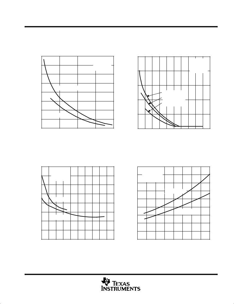
TLC271, TLC271A, TLC271B
LinCMOS PROGRAMMABLE LOW-POWER
OPERATIONAL AMPLIFIERS
SLOS090C ± NOVEMBER 1987 ± REVISED AUGUST 1997
TYPICAL CHARACTERISTICS (HIGH-BIAS MODE)²
|
|
LOW-LEVEL OUTPUT VOLTAGE |
|
||
|
|
|
vs |
|
|
|
|
COMMON-MODE INPUT VOLTAGE |
|
||
|
700 |
|
|
VDD = 5 V |
|
|
|
|
|
|
|
mV |
650 |
|
|
IOL = 5 mA |
|
|
|
TA = 25°C |
|
||
|
|
|
|
||
± |
|
|
|
|
|
Voltage |
600 |
|
|
|
|
|
|
|
|
|
|
Output |
550 |
VÎÎÎÎ= ± 100 mV |
|
|
|
500 |
|
|
|||
|
|
ID |
|
|
|
Level |
450 |
|
|
|
|
Low- |
400 |
|
|
|
|
± |
|
|
|
|
|
ÁÁOL |
|
VID = ± 1 V |
|
|
|
VOL |
350 |
|
|
|
|
|
|
|
|
|
|
|
300 |
|
|
|
4 |
|
0 |
1 |
2 |
3 |
|
|
|
VIC ± Common-Mode Input Voltage ± V |
|
||
Figure 10
LOW-LEVEL OUTPUT VOLTAGE vs
COMMON-MODE INPUT VOLTAGE
|
500 |
|
|
|
|
|
|
|
|
|
|
|
|
|
|
|
|
|
|
|
VDD = 10 V |
|
|
mV |
|
|
|
|
|
|
|
|
IOL = 5 mA |
|
|
450 |
|
|
|
|
|
|
|
TA = 25°C |
|
||
± |
|
|
|
|
|
|
|
|
|||
Voltage |
|
|
|
|
|
|
|
|
|
|
|
400 |
|
|
|
|
|
|
|
|
|
|
|
Output |
|
|
|
|
|
|
|
|
|
|
|
|
|
|
|
VID = ± 100 mV |
|
|
|
|
|||
-Level |
350 |
|
|
|
VID = ± 1 V |
|
|
|
|
|
|
|
|
|
VID = ± 2.5 V |
|
|
|
|
||||
|
|
|
|
|
|
|
|
||||
Á±LowOL |
300 |
|
|
|
|
|
|
|
|
|
|
VOL |
|
|
|
|
|
|
|
|
|
|
|
Á |
|
|
|
|
|
|
|
|
|
|
|
|
250 |
1 |
2 |
3 |
4 |
5 |
6 |
7 |
8 |
9 |
10 |
|
0 |
||||||||||
|
|
VIC ± Common-Mode Input Voltage ± V |
|
|
|||||||
Figure 11
|
LOW-LEVEL OUTPUT VOLTAGE |
|
|
vs |
|
|
DIFFERENTIAL INPUT VOLTAGE |
|
|
800 |
|
|
IOL = 5 mA |
|
|
VIC = VID/2 |
|
mV± |
700 |
|
TA = 25°C |
||
|
||
Voltage |
600 |
|
500 |
||
Output |
ÎÎÎV = 5 V |
|
|
DD |
|
Level- |
400 |
|
300 |
||
|
||
Low |
VDD = 10 V |
|
200 |
||
ÁÁ±OL |
100 |
|
VOL |
||
|
0 |
|
|
0 ± 1 ± 2 ± 3 ± 4 ± 5 ± 6 ± 7 ± 8 ± 9 ± 10 |
|
|
VID ± Differential Input Voltage ± V |
Figure 12
LOW-LEVEL OUTPUT VOLTAGE vs
FREE-AIR TEMPERATURE
|
900 |
|
± mV |
800 |
|
700 |
||
Voltage |
||
600 |
||
|
||
Output |
500 |
|
400 |
||
-Level |
||
300 |
||
Low |
||
200 |
||
Á±OL |
||
|
||
VOL |
|
Á 100
IOL = 5 mA VID = ± 1 V VIC = 0.5 V
ÎÎÎV = 5 V
DD
VÎÎÎ= 10 V
DD
0
± 75 ± 50 ± 25 0 25 50 75 100 125 TA ± Free-Air Temperature ± °C
Figure 13
² Data at high and low temperatures are applicable only within the rated operating free-air temperature ranges of the various devices.
POST OFFICE BOX 655303 •DALLAS, TEXAS 75265 |
15 |
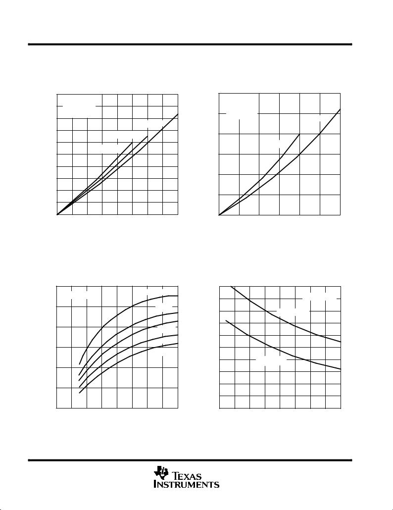
TLC271, TLC271A, TLC271B
LinCMOS PROGRAMMABLE LOW-POWER
OPERATIONAL AMPLIFIERS
SLOS090C ± NOVEMBER 1987 ± REVISED AUGUST 1997
TYPICAL CHARACTERISTICS (HIGH-BIAS MODE)²
|
|
|
LOW-LEVEL OUTPUT VOLTAGE |
|
|||||
|
|
|
|
|
vs |
|
|
|
|
|
|
LOW-LEVEL OUTPUT CURRENT |
|
||||||
|
1 |
VID = ± 1 V |
|
|
|
|
|
|
|
|
|
|
|
|
|
|
|
||
mV± |
0.9 |
VIC = 0.5 V |
|
|
|
|
|
|
|
0.8 |
TA = 25°C |
|
|
|
|
|
|
||
|
|
|
|
|
|
|
|
||
Voltage |
0.7 |
|
|
|
|
|
VDD = 5 V |
|
|
|
|
|
ÎÎÎÎV = 4 V |
|
|
||||
|
|
|
|
|
|
||||
|
|
|
|
|
|
|
|||
|
|
|
|
|
DD |
|
|
|
|
Output |
0.6 |
|
|
VDD = 3 V |
|
|
|
|
|
0.5 |
|
|
|
|
|
|
|||
|
|
|
|
|
|
|
|||
Level- |
|
|
|
|
|
|
|
|
|
0.4 |
|
|
|
|
|
|
|
|
|
Á±LowOL |
|
|
|
|
|
|
|
|
|
0.2 |
|
|
|
|
|
|
|
|
|
|
0.3 |
|
|
|
|
|
|
|
|
VOL |
0.1 |
|
|
|
|
|
|
|
|
|
|
|
|
|
|
|
|
|
|
|
0 |
|
|
|
|
|
|
|
8 |
|
0 |
1 |
2 |
3 |
4 |
5 |
6 |
7 |
|
|
|
IOL ± Low-Level Output Current ± mA |
|
||||||
Figure 14
|
|
LOW-LEVEL OUTPUT VOLTAGE |
|
||||
|
|
|
|
vs |
|
|
|
|
|
LOW-LEVEL OUTPUT CURRENT |
|
||||
|
3 |
VID = ±1 V |
|
|
|
|
|
|
|
|
|
|
|
|
|
mV |
|
VIC = 0.5 V |
|
|
|
|
|
2.5 |
TA = 25°C |
|
|
VDD = 16 V |
|
||
± |
|
|
|
|
|
||
Voltage |
2 |
|
|
|
|
|
|
Output |
1.5 |
|
VDD = 10 V |
|
|
|
|
|
|
|
|
|
|
||
-Level |
1 |
|
|
|
|
|
|
± Low |
|
|
|
|
|
|
|
|
|
|
|
|
|
|
|
ÁÁOL |
0.5 |
|
|
|
|
|
|
VOL |
|
|
|
|
|
|
|
|
0 |
|
|
|
|
|
|
|
0 |
5 |
10 |
15 |
20 |
25 |
30 |
|
|
IOL ± Low-Level Output Current ± mA |
|
||||
Figure 15
|
|
|
|
|
LARGE-SIGNAL |
|
|
|
||
|
|
|
DIFFERENTIAL VOLTAGE AMPLIFICATION |
|||||||
|
|
|
|
|
|
vs |
|
|
|
|
|
|
|
|
|
SUPPLY VOLTAGE |
|
|
|||
|
|
60 |
ÎÎ |
|
|
|
T |
= ± 55°C |
|
|
|
|
|
|
|
|
|
||||
|
|
|
RL = 10 kΩ |
|
|
|
A |
|
|
|
DifferentialSignal-Large |
Amplification± V/mV |
50 |
|
|
|
|
|
|
Î0°C |
|
|
|
|
|
|
|
|
|
|||
40 |
|
|
|
|
|
|
ÎÎ25°C |
|||
|
|
|
|
|
|
|
|
|||
|
|
|
|
|
|
|
|
|
85°C |
|
|
|
30 |
|
|
|
|
|
|
125°C |
|
VD Voltage |
|
|
|
|
|
|
|
|
||
20 |
|
|
|
|
|
|
|
|
||
± |
|
|
|
|
|
|
|
|
|
|
|
|
|
|
|
|
|
|
|
|
|
ÁVDA |
|
|
|
|
|
|
|
|
|
|
|
|
10 |
|
|
|
|
|
|
|
|
|
|
0 |
|
|
|
|
|
|
|
|
|
|
0 |
2 |
4 |
6 |
8 |
10 |
12 |
14 |
16 |
|
|
|
|
VDD ± Supply Voltage ± V |
|
|
||||
Figure 16
LARGE-SIGNAL
DIFFERENTIAL VOLTAGE AMPLIFICATION vs
FREE-AIR TEMPERATURE
|
|
50 |
|
|
|
|
|
|
|
|
|
|
45 |
|
|
|
|
|
RL = 10 kΩ |
|
|
DifferentialSignal-Large |
V/mV±Amplification |
40 |
|
|
|
VDD = 10 V |
|
|
||
|
|
|
|
|
|
|
||||
|
|
35 |
|
|
|
|
|
|
|
|
|
|
30 |
|
|
|
|
|
|
|
|
|
|
25 |
|
|
|
|
|
|
|
|
ÁVDA |
Voltage |
20 |
|
|
VDD = 5 V |
|
|
|
|
|
10 |
|
|
|
|
|
|
|
|
||
± |
|
15 |
|
|
|
|
|
|
|
|
VD |
|
|
|
|
|
|
|
|
|
|
|
|
|
|
|
|
|
|
|
|
|
|
|
5 |
|
|
|
|
|
|
|
|
|
|
0 |
|
|
|
|
|
|
|
|
|
|
± 75 |
± 50 |
± 25 |
0 |
25 |
50 |
75 |
100 |
125 |
|
|
|
|
TA ± Free-Air Temperature ± °C |
|
|
||||
Figure 17
² Data at high and low temperatures are applicable only within the rated operating free-air temperature ranges of the various devices.
16 |
POST OFFICE BOX 655303 •DALLAS, TEXAS 75265 |

TLC271, TLC271A, TLC271B
LinCMOS PROGRAMMABLE LOW-POWER
OPERATIONAL AMPLIFIERS
SLOS090C ± NOVEMBER 1987 ± REVISED AUGUST 1997
TYPICAL CHARACTERISTICS (HIGH-BIAS MODE)²
INPUT BIAS CURRENT AND INPUT OFFSET |
COMMON-MODE INPUT VOLTAGE |
CURRENT |
(POSITIVE LIMIT) |
vs |
vs |
FREE-AIR TEMPERATURE |
SUPPLY VOLTAGE |
|
10000 |
ÁÁÁV = 10 V |
|
|
|
|
16 |
|
|
|
|
|
|
|
|
|
|
DD |
|
|
|
|
|
|
|
VIC = 5 V |
|
|
|
±V |
14 |
|
|
ÁÁÁ |
|
|
|
||
|
|
See Note A |
|
|
|
± Common-Mode Input Voltage |
|
and |
1000 |
|
|
|
|
|
|
|
|
|
IIB |
|
12 |
||
|
|
|
|
|
|||
Bias |
|
|
|
|
|
||
100 |
|
|
|
|
10 |
||
Input |
|
|
|
|
|
||
|
|
|
|
IIO |
8 |
||
± |
|
|
|
|
|
||
|
|
|
|
|
|
||
IO |
|
|
|
|
|
|
|
IO |
10 |
|
|
|
|
6 |
|
and |
CurrentsInputOffsetnA± |
|
|
|
|
||
|
|
|
|
|
|||
IB |
|
|
|
|
|
||
IIB |
|
|
|
|
4 |
||
|
1 |
|
|
|
|
IC |
|
|
|
|
|
|
|
|
|
|
|
|
|
|
|
V |
2 |
|
|
|
|
|
|
|
|
|
0.1 |
|
|
|
|
|
0 |
|
25 |
45 |
65 |
85 |
105 |
125 |
|
|
|
TA ± Free-Air Temperature ± °C |
|
|
|||
NOTE A: The typical values of input bias current and input offset current below 5 pA were determined mathematically.
TA = 25°C
0 |
2 |
4 |
6 |
8 |
10 |
12 |
14 |
16 |
|
|
VDD ± Supply Voltage ± V |
|
|
||||
Figure 18
SUPPLY CURRENT
|
|
|
|
|
vs |
|
|
|
|
|
|
|
SUPPLY VOLTAGE |
|
|
||||
|
2.5 |
|
|
|
|
|
|
|
|
|
|
ÎÎÎÎV = V /2 |
|
|
|
|
|
|
|
|
|
O |
DD |
|
|
|
|
|
|
|
|
No Load |
|
|
|
|
|
|
|
|
2 |
ÎÎÎÎ |
|
|
|
TA =± 55°C |
|
||
± mA |
|
|
|
|
|
|
|||
|
|
|
|
|
|
|
|
|
|
Current |
1.5 |
|
|
|
|
|
|
Î0°C |
|
|
|
|
|
|
|
|
25°C |
|
|
Supply |
|
|
|
|
|
|
|
|
|
1 |
|
|
|
|
|
|
70°C |
|
|
|
|
|
|
|
|
|
|
||
± |
|
|
|
|
|
|
|
|
|
|
|
|
|
|
|
|
|
|
|
ÁDD |
|
|
|
|
|
|
|
125°C |
|
IDD |
|
|
|
|
|
|
|
|
|
Á 0.5 |
|
|
|
|
|
|
|
|
|
|
0 |
|
|
|
|
|
|
|
16 |
|
0 |
2 |
4 |
6 |
8 |
10 |
12 |
14 |
|
|
|
|
VDD ± Supply Voltage ± V |
|
|
||||
Figure 20
Figure 19
SUPPLY CURRENT vs
FREE-AIR TEMPERATURE
|
2 |
|
|
|
|
|
|
|
|
|
|
ÎÎÎV = V /2 |
|
|
|
|
|
|
|
|
|
O |
DD |
|
|
|
|
|
|
|
|
No Load |
|
|
|
|
|
|
|
|
|
ÎÎÎ |
|
|
|
|
|
|
|
± mA |
1.5 |
|
|
|
|
|
|
|
|
|
|
|
|
|
|
|
|
|
|
Current |
1 |
|
|
|
|
VDD = 10 V |
|
|
|
|
|
|
|
|
|
|
|
||
± Supply |
|
|
|
|
|
|
|
|
|
|
|
VDD = 5 V |
|
|
|
|
|
||
ÁDD |
0.5 |
|
|
|
|
|
|
||
|
|
|
|
|
|
|
|
||
DDI |
|
|
|
|
|
|
|
|
|
|
0 |
|
|
|
|
|
|
|
|
|
± 75 |
± 50 |
± 25 |
0 |
25 |
50 |
75 |
100 |
125 |
|
|
|
TA ± Free-Air Temperature ± °C |
|
|
||||
Figure 21
² Data at high and low temperatures are applicable only within the rated operating free-air temperature ranges of the various devices.
POST OFFICE BOX 655303 •DALLAS, TEXAS 75265 |
17 |

TLC271, TLC271A, TLC271B
LinCMOS PROGRAMMABLE LOW-POWER
OPERATIONAL AMPLIFIERS
SLOS090C ± NOVEMBER 1987 ± REVISED AUGUST 1997
TYPICAL CHARACTERISTICS (HIGH-BIAS MODE)²
|
|
|
|
SLEW RATE |
|
|
|
|
|
|
|
SLEW RATE |
|
|
|
||||
|
|
|
|
|
vs |
|
|
|
|
|
|
|
|
|
vs |
|
|
|
|
|
|
|
|
SUPPLY VOLTAGE |
|
|
|
|
|
|
FREE-AIR TEMPERATURE |
|
|
||||||
|
8 |
AV = 1 |
|
|
|
|
|
|
|
|
8 |
|
|
|
|
|
AV = 1 |
|
|
|
|
|
|
|
|
|
|
|
|
|
|
|
|
|
|
|
|
||
|
7 |
VI(PP) = 1 V |
|
|
|
|
|
|
7 |
|
|
VDD = 10 V |
|
RL = 10 kΩ |
|
||||
|
RL = 10 kΩ |
|
|
|
|
|
|
|
|
|
|
CL = 20 pF |
|
||||||
|
|
CL = 20 pF |
|
|
|
|
|
|
|
|
|
|
VI(PP) = 5.5 V |
See Figure 99 |
|||||
V/ us |
6 |
TA = 25°C |
|
|
|
|
|
|
V/ us |
6 |
|
|
|
|
|
|
|
|
|
|
See Figure 98 |
|
|
|
|
|
|
|
|
|
|
|
VDD = 10 V |
|
|||||
5 |
|
|
|
|
|
|
|
|
5 |
|
|
|
|
|
|
||||
± |
|
|
|
|
|
|
|
|
± |
|
|
|
|
|
VI(PP) = 1 V |
||||
Rate |
|
|
|
|
|
|
|
|
|
Rate |
|
|
|
|
|
|
|||
4 |
|
|
|
|
|
|
|
|
4 |
|
|
|
|
|
|
|
|
||
± Slew |
|
|
|
|
|
|
|
|
± Slew |
|
|
|
|
|
|
|
|
||
3 |
|
|
|
|
|
|
|
|
3 |
|
|
|
|
|
|
|
|
||
SR |
2 |
|
|
|
|
|
|
|
|
SR |
2 |
|
VDD = 5 V |
|
|
|
|
|
|
|
|
|
|
|
|
|
|
|
|
|
|
|
|
|
|
||||
|
|
|
|
|
|
|
|
|
|
|
|
|
VI(PP) = 1 V |
|
|
|
|
|
|
|
1 |
|
|
|
|
|
|
|
|
|
1 |
|
|
|
|
VDD = 5 V |
|
|
|
|
|
|
|
|
|
|
|
|
|
|
|
|
|
|
|
VI(PP) = 2.5 V |
|
||
|
0 |
|
|
|
|
|
|
|
|
|
0 |
|
|
|
|
|
|
|
|
|
0 |
2 |
4 |
6 |
8 |
10 |
12 |
14 |
16 |
|
± 75 |
± 50 |
± 25 |
0 |
25 |
50 |
75 |
100 |
125 |
|
|
|
VDD ± Supply Voltage ± V |
|
|
|
|
|
T ± Free-Air Temperature ± °C |
|
|
||||||||
|
|
|
|
|
|
|
|
|
|
|
|
|
A |
|
|
|
|
|
|
|
|
|
|
Figure 22 |
|
|
|
|
|
|
|
|
Figure 23 |
|
|
|
|
||
|
|
|
BIAS-SELECT CURRENT |
|
|
|
||||
|
|
|
|
|
vs |
|
|
|
|
|
|
|
|
|
SUPPLY VOLTAGE |
|
|
|
|
||
|
± 3 |
|
|
|
|
|
|
|
V |
10 |
|
|
|
|
|
|
|
|
± |
||
|
|
|
|
|
|
|
TA |
= 25°C |
|
|
|
± 2.7 |
|
|
|
|
|
Voltage |
9 |
||
|
|
|
|
|
|
VI(SEL) = 0 |
||||
|
|
|
|
|
|
|
||||
|
|
|
|
|
|
|
|
|
||
±uaA |
± 2.4 |
|
|
|
|
|
|
|
Output |
8 |
± 2.1 |
|
|
|
|
|
|
|
7 |
||
Current |
|
|
|
|
|
|
|
Peak-to |
||
± 1.5 |
|
|
|
|
|
|
|
5 |
||
Select-Bias |
± 1.8 |
|
|
|
|
|
|
|
PeakMaximum- |
6 |
± 1.2 |
|
|
|
|
|
|
|
4 |
||
|
|
|
|
|
|
|
|
|
||
|
± 0.9 |
|
|
|
|
|
|
|
|
3 |
|
± 0.6 |
|
|
|
|
|
|
|
|
2 |
|
|
|
|
|
|
|
|
|
± |
1 |
|
± 0.3 |
|
|
|
|
|
|
|
O(PP) |
|
|
|
|
|
|
|
|
|
|
||
|
0 |
2 |
4 |
6 |
8 |
10 |
12 |
14 |
V |
0 |
|
0 |
16 |
10 |
|||||||
|
|
|
VDD ± Supply Voltage ± V |
|
|
|
||||
Figure 24
MAXIMUM PEAK-TO-PEAK OUTPUT
|
VOLTAGE |
|
|
vs |
|
FREQUENCY |
|
|
VDD = 10 V |
|
|
|
TA = 125°C |
|
|
TA = 25°C |
|
|
TA = 55°C |
|
VDD = 5 V |
|
|
RL = 10 kΩ |
|
|
See Figure 98 |
|
|
100 |
1000 |
10000 |
f ± Frequency ± kHz |
|
|
Figure 25
² Data at high and low temperatures are applicable only within the rated operating free-air temperature ranges of the various devices.
18 |
POST OFFICE BOX 655303 •DALLAS, TEXAS 75265 |

TLC271, TLC271A, TLC271B
LinCMOS PROGRAMMABLE LOW-POWER
OPERATIONAL AMPLIFIERS
SLOS090C ± NOVEMBER 1987 ± REVISED AUGUST 1997
TYPICAL CHARACTERISTICS (HIGH-BIAS MODE)²
UNITY-GAIN BANDWIDTH vs
FREE-AIR TEMPERATURE
|
3 |
|
|
|
|
|
VDD = 5 V |
|
|
|
|
|
|
|
|
|
|
||
|
|
|
|
|
|
|
VI = 10 mV |
|
|
MHz |
|
|
|
|
|
|
CL = 20 pF |
|
|
|
|
|
|
|
|
See Figure 100 |
|
||
2.5 |
|
|
|
|
|
|
|
|
|
Bandwidth ± |
|
|
|
|
|
|
|
|
|
2 |
|
|
|
|
|
|
|
|
|
± Unity-Gain |
|
|
|
|
|
|
|
|
|
1.5 |
|
|
|
|
|
|
|
|
|
1 |
|
|
|
|
|
|
|
|
|
1B |
|
|
|
|
|
|
|
|
|
|
1 |
|
|
|
|
|
|
|
|
|
± 75 |
± 50 |
± 25 |
0 |
25 |
50 |
75 |
100 |
125 |
|
|
|
TA ± Free-Air Temperature ± °C |
|
|
||||
UNITY-GAIN BANDWIDTH
|
|
|
|
|
vs |
|
|
|
|
|
|
|
|
SUPPLY VOLTAGE |
|
|
|
||
|
2.5 |
VI = 10 mV |
|
|
|
|
|
|
|
|
|
|
|
|
|
|
|
||
|
|
CL = 20 pF |
|
|
|
|
|
|
|
± MHz |
|
TA = 25°C |
|
|
|
|
|
|
|
|
See Figure 100 |
|
|
|
|
|
|||
|
|
|
|
|
|
|
|
|
|
-Gain Bandwidth |
2 |
|
|
|
|
|
|
|
|
|
|
|
|
|
|
|
|
|
|
± Unity |
1.5 |
|
|
|
|
|
|
|
|
|
|
|
|
|
|
|
|
|
|
1 |
|
|
|
|
|
|
|
|
|
1B |
|
|
|
|
|
|
|
|
|
|
1 |
|
|
|
|
|
|
|
|
|
0 |
2 |
4 |
6 |
8 |
10 |
12 |
14 |
16 |
|
|
|
VDD ± Supply Voltage ± V |
|
|
||||
Figure 26 |
Figure 27 |
LARGE-SIGNAL DIFFERENTIAL VOLTAGE AMPLIFICATION AND PHASE SHIFT
vs
|
|
|
|
FREQUENCY |
|
|
|
||
|
|
107 |
VDD = 5 V |
|
|
|
|
|
|
|
|
|
|
|
|
|
|
|
|
|
|
6 |
RL = 10 kΩ |
|
|
|
|
|
|
|
|
10 |
TA = 25°C |
|
|
|
|
|
|
± Large-Signal Differential |
|
|
|
|
|
|
|
|
|
Voltage Amplification |
105 |
|
|
|
|
|
0° |
|
|
104 |
|
|
|
|
|
30° |
Phase Shift |
||
103 |
|
|
AVD |
|
|
|
|||
|
|
|
|
|
60° |
||||
102 |
|
|
|
|
|
90° |
|||
|
Phase Shift |
|
|
|
|||||
VD |
|
101 |
|
|
|
|
|
120° |
|
VDA |
|
|
|
|
|
|
|
|
|
|
|
1 |
|
|
|
|
|
150° |
|
|
|
0.1 |
100 |
1 k |
10 k |
100 k |
1 M |
180° |
|
|
|
10 |
10 M |
|
|||||
|
|
|
|
f ± Frequency ± Hz |
|
|
|
||
Figure 28
² Data at high and low temperatures are applicable only within the rated operating free-air temperature ranges of the various devices.
POST OFFICE BOX 655303 •DALLAS, TEXAS 75265 |
19 |

TLC271, TLC271A, TLC271B
LinCMOS PROGRAMMABLE LOW-POWER
OPERATIONAL AMPLIFIERS
SLOS090C ± NOVEMBER 1987 ± REVISED AUGUST 1997
TYPICAL CHARACTERISTICS (HIGH-BIAS MODE)²
LARGE-SCALE DIFFERENTIAL VOLTAGE AMPLIFICATION AND PHASE SHIFT
vs
|
|
|
|
FREQUENCY |
|
|
|
||
|
|
107 |
VDD = 10 V |
|
|
|
|
|
|
|
|
106 |
RL = 10 kΩ |
|
|
|
|
|
|
|
|
TA = 25°C |
|
|
|
|
|
|
|
± Large-Signal Differential |
|
|
|
|
|
|
|
|
|
Voltage Amplification |
105 |
|
|
|
|
|
0° |
|
|
104 |
|
|
|
|
|
30° |
Phase Shift |
||
103 |
|
|
AVD |
|
|
|
|||
|
|
|
|
|
60° |
||||
102 |
|
|
|
|
|
90° |
|||
|
Phase Shift |
|
|
|
|||||
VD |
|
101 |
|
|
|
|
|
120° |
|
VDA |
|
|
|
|
|
|
|
|
|
|
|
1 |
|
|
|
|
|
150° |
|
|
|
0.1 |
100 |
1 k |
10 k |
100 k |
1 M |
180° |
|
|
|
10 |
10 M |
|
|||||
|
|
|
|
f ± Frequency ± Hz |
|
|
|
||
Figure 29
PHASE MARGIN |
PHASE MARGIN |
|
|
|
|
|
vs |
|
|
|
|
|
|
|
|
|
vs |
|
|
|
|
|
|
|
|
SUPPLY VOLTAGE |
|
|
|
|
|
|
FREE-AIR TEMPERATURE |
|
|
||||||
|
53° |
|
|
|
|
|
|
|
|
|
50° |
|
|
|
|
|
|
|
|
|
52° |
|
|
|
|
|
|
|
|
|
|
|
|
|
|
|
VDD = 5 V |
|
|
|
|
|
|
|
|
|
|
|
|
|
|
|
|
|
|
VI = 10 mV |
|
||
|
|
|
|
|
|
|
|
|
|
|
|
|
|
|
|
|
|
||
|
51° |
|
|
|
|
|
|
|
|
|
48° |
|
|
|
|
|
CL = 20 pF |
|
|
Margin |
|
|
|
|
|
|
|
|
Margin |
|
|
|
|
|
|
See Figure 100 |
|||
50° |
|
|
|
|
|
|
|
|
46° |
|
|
|
|
|
|
|
|
||
|
|
|
|
|
|
|
|
|
|
|
|
|
|
|
|
|
|
||
Phase± |
|
|
|
|
|
|
|
|
|
Phase± |
|
|
|
|
|
|
|
|
|
49° |
|
|
|
|
|
|
|
|
44° |
|
|
|
|
|
|
|
|
||
|
|
|
|
|
|
|
|
|
|
|
|
|
|
|
|
|
|
|
|
m |
48° |
|
|
|
|
|
|
|
|
m |
|
|
|
|
|
|
|
|
|
|
|
|
|
|
|
|
|
|
|
|
|
|
|
|
|
|
|
||
mφ |
|
|
|
|
|
VI = 10 mV |
|
|
mφ |
|
|
|
|
|
|
|
|
|
|
|
47° |
|
|
|
|
|
|
|
|
|
|
|
|
|
|
|
|
||
|
|
|
|
|
|
CL = 20 pF |
|
|
|
42° |
|
|
|
|
|
|
|
|
|
|
46° |
|
|
|
|
TA = 25°C |
|
|
|
|
|
|
|
|
|
|
|
|
|
|
|
|
|
|
See Figure 100 |
|
|
|
|
|
|
|
|
|
|
|
|||
|
|
|
|
|
|
|
|
|
|
|
|
|
|
|
|
|
|||
|
45° |
|
|
|
|
|
|
|
16 |
|
40° |
|
|
|
|
|
|
|
|
|
0 |
2 |
4 |
6 |
8 |
10 |
12 |
14 |
|
± 75 |
± 50 |
± 25 |
0 |
25 |
50 |
75 |
100 |
125 |
|
|
|
|
VDD ± Supply Voltage ± V |
|
|
|
|
|
TA ± Free-Air Temperature ± °C |
|
|
||||||||
Figure 30 |
Figure 31 |
² Data at high and low temperatures are applicable only within the rated operating free-air temperature ranges of the various devices.
20 |
POST OFFICE BOX 655303 •DALLAS, TEXAS 75265 |
TLC271, TLC271A, TLC271B
LinCMOS PROGRAMMABLE LOW-POWER
OPERATIONAL AMPLIFIERS
SLOS090C ± NOVEMBER 1987 ± REVISED AUGUST 1997
TYPICAL CHARACTERISTICS (HIGH-BIAS MODE)²
PHASE MARGIN |
EQUIVALENT NOISE VOLTAGE |
|
|
|
|
vs |
|
|
|
|
|
vs |
|
|
|
|
CAPACITIVE LOAD |
|
|
|
|
FREQUENCY |
|
||
|
50° |
|
|
|
|
|
|
400 |
|
|
|
|
|
|
|
|
VDD = 5 mV |
|
Hz |
|
|
VDD = 5 V |
|
|
45° |
|
|
|
|
nV/Hz± |
350 |
|
|
||
|
|
|
|
TA = 25°C |
|
|
TA = 25°C |
|
|||
|
|
|
|
|
VI = 10 mV |
|
|
|
|
RS = 20 Ω |
|
MarginPhase |
|
|
|
|
See Figure 100 |
VoltageNoise |
300 |
|
See Figure 99 |
|
|
|
|
|
|
|
|
|
|
|
|||
|
|
|
|
|
|
|
|
|
|
|
|
|
40° |
|
|
|
|
|
|
250 |
|
|
|
|
|
|
|
|
|
|
|
|
|
|
|
|
|
|
|
|
|
|
EquivalentInput |
200 |
|
|
|
φm |
35° |
|
|
|
|
|
|
|
|
|
|
± |
|
|
|
|
|
|
150 |
|
|
|
|
m |
|
|
|
|
|
|
|
|
|
|
|
|
|
|
|
|
|
|
|
|
|
|
|
|
30° |
|
|
|
|
|
|
100 |
|
|
|
|
|
|
|
|
|
|
|
|
|
|
|
|
|
|
|
|
|
|
± |
50 |
|
|
|
|
|
|
|
|
|
|
n |
|
|
|
|
|
25° |
|
|
|
|
|
VN |
0 |
|
|
|
|
|
|
|
|
|
|
|
|
|
||
|
0 |
20 |
40 |
60 |
80 |
100 |
|
1 |
10 |
100 |
1000 |
|
|
|
CL ± Capacitive Load ± pF |
|
|
|
f ± Frequency ± Hz |
|
|||
Figure 32 |
Figure 33 |
² Data at high and low temperatures are applicable only within the rated operating free-air temperature ranges of the various devices.
POST OFFICE BOX 655303 •DALLAS, TEXAS 75265 |
21 |

TLC271, TLC271A, TLC271B
LinCMOS PROGRAMMABLE LOW-POWER
OPERATIONAL AMPLIFIERS
SLOS090C ± NOVEMBER 1987 ± REVISED AUGUST 1997
MEDIUM-BIAS MODE
electrical characteristics at specified free-air temperature (unless otherwise noted)
|
|
|
|
|
TLC271C, TLC271AC, TLC271BC |
|
|
||||||
|
|
|
|
T ² |
|
|
|
|
|
|
|
|
|
|
PARAMETER |
TEST CONDITIONS |
V |
DD |
= 5 V |
|
V |
DD |
= 10 V |
|
UNIT |
||
|
|
|
|
A |
|
|
|
|
|
|
|
||
|
|
|
|
|
MIN |
TYP |
MAX |
MIN |
|
TYP |
MAX |
|
|
|
|
|
|
|
|
|
|
|
|
|
|
|
|
|
|
TLC271C |
|
25°C |
|
|
1.1 |
10 |
|
|
1.1 |
10 |
|
|
|
VO = 1.4 V, |
Full range |
|
|
|
12 |
|
|
|
12 |
|
|
|
|
|
|
|
|
|
|
|
|
||||
|
|
|
|
|
|
|
|
|
|
|
|
|
|
|
|
|
25°C |
|
|
0.9 |
5 |
|
|
0.9 |
5 |
|
|
VIO |
Input offset voltage |
TLC271AC |
VIC = 0 |
|
|
|
|
mV |
|||||
RS = 50 Ω, |
Full range |
|
|
|
6.5 |
|
|
|
6.5 |
||||
|
|
|
RI = 100 kΩ |
|
|
|
|
|
|
|
|
|
|
|
|
TLC271BC |
25°C |
|
0.25 |
2 |
|
|
0.26 |
2 |
|
||
|
|
|
Full range |
|
|
|
3 |
|
|
|
3 |
|
|
|
|
|
|
|
|
|
|
|
|
|
|||
|
|
|
|
|
|
|
|
|
|
|
|
|
|
αVIO |
Average temperature coefficient |
|
25°C to |
|
|
1.7 |
|
|
|
2.1 |
|
µV/°C |
|
of input offset voltage |
|
70°C |
|
|
|
|
|
|
|||||
|
|
|
|
|
|
|
|
|
|
|
|||
|
|
|
|
|
|
|
|
|
|
|
|
|
|
IIO |
Input offset current (see Note 4) |
VO = VDD /2, |
25°C |
|
|
0.1 |
|
|
|
0.1 |
|
pA |
|
VIC = VDD /2 |
70°C |
|
|
7 |
300 |
|
|
7 |
300 |
||||
|
|
|
|
|
|
|
|
||||||
IIB |
Input bias current (see Note 4) |
VO = VDD /2, |
25°C |
|
|
0.6 |
|
|
|
0.7 |
|
pA |
|
VIC = VDD /2 |
70°C |
|
|
40 |
600 |
|
|
50 |
600 |
||||
|
|
|
|
|
|
|
|
||||||
|
|
|
|
|
± 0.2 |
± 0.3 |
|
± 0.2 |
|
±0.3 |
|
|
|
|
|
|
|
25°C |
to |
|
to |
|
to |
|
to |
|
V |
VICR |
Common-mode input |
|
|
4 |
|
4.2 |
|
9 |
|
9.2 |
|
|
|
voltage range (see Note 5) |
|
|
± 0.2 |
|
|
|
± 0.2 |
|
|
|
|
||
|
|
|
|
|
|
|
|
|
|
||||
|
|
|
|
Full range |
to |
|
|
|
to |
|
|
|
V |
|
|
|
|
|
3.5 |
|
|
|
8.5 |
|
|
|
|
|
|
|
|
|
|
|
|
|
|
|
|
|
|
|
|
|
VID = 100 mV, |
25°C |
3.2 |
|
3.9 |
|
8 |
|
8.7 |
|
|
|
|
|
|
|
|
|
|
|
|
|
|
|
|
VOH |
High-level output voltage |
0°C |
3 |
|
3.9 |
|
7.8 |
|
8.7 |
|
V |
||
RL = 100 kΩ |
|
|
|
|
|||||||||
|
|
|
70°C |
3 |
|
4 |
|
7.8 |
|
8.7 |
|
|
|
|
|
|
|
|
|
|
|
|
|||||
|
|
|
|
|
|
|
|
|
|
|
|
|
|
|
|
|
VID = ±100 mV, |
25°C |
|
|
0 |
50 |
|
|
0 |
50 |
|
VOL |
Low-level output voltage |
0°C |
|
|
0 |
50 |
|
|
0 |
50 |
mV |
||
IOL = 0 |
|
|
|
|
|||||||||
|
|
|
70°C |
|
|
0 |
50 |
|
|
0 |
50 |
|
|
|
|
|
|
|
|
|
|
|
|||||
|
|
|
|
|
|
|
|
|
|
|
|
|
|
|
Large-signal differential |
RL = 100 kΩ, |
25°C |
25 |
|
170 |
|
25 |
|
275 |
|
|
|
|
|
|
|
|
|
|
|
|
|
|
|||
AVD |
0°C |
15 |
|
200 |
|
15 |
|
320 |
|
V/mV |
|||
voltage amplification |
See Note 6 |
|
|
|
|
||||||||
|
70°C |
15 |
|
140 |
|
15 |
|
230 |
|
|
|||
|
|
|
|
|
|
|
|
|
|||||
|
|
|
|
25°C |
65 |
|
91 |
|
65 |
|
94 |
|
|
|
|
|
|
|
|
|
|
|
|
|
|
|
|
CMRR |
Common-mode rejection ratio |
VIC = VICRmin |
0°C |
60 |
|
91 |
|
60 |
|
94 |
|
dB |
|
|
|
|
|
70°C |
60 |
|
92 |
|
60 |
|
94 |
|
|
|
|
|
|
|
|
|
|
|
|
|
|
|
|
|
Supply-voltage rejection ratio |
VDD = 5 V to 10 V |
25°C |
70 |
|
93 |
|
70 |
|
93 |
|
|
|
kSVR |
0°C |
60 |
|
92 |
|
60 |
|
92 |
|
dB |
|||
( VDD / VIO) |
VO = 1.4 V |
|
|
|
|
||||||||
|
70°C |
60 |
|
94 |
|
60 |
|
94 |
|
|
|||
|
|
|
|
|
|
|
|
|
|||||
II(SEL) |
Input current (BIAS SELECT) |
VI(SEL) = VDD /2 |
25°C |
|
± 130 |
|
|
± 160 |
|
nA |
|||
|
|
|
VO = VDD /2, |
25°C |
|
|
105 |
280 |
|
|
143 |
300 |
|
IDD |
Supply current |
VIC = VDD /2, |
0°C |
|
|
125 |
320 |
|
|
173 |
400 |
µA |
|
|
|
|
No load |
70°C |
|
|
85 |
220 |
|
|
110 |
280 |
|
|
|
|
|
|
|
|
|
|
|||||
|
|
|
|
|
|
|
|
|
|
|
|
|
|
² Full range is 0°C to 70°C.
NOTES: 4. The typical values of input bias current and input offset current below 5 pA were determined mathematically.
5.This range also applies to each input individually.
6.At VDD = 5 V, VO = 0.25 V to 2 V; at VDD = 10 V, VO = 1 V to 6 V.
22 |
POST OFFICE BOX 655303 •DALLAS, TEXAS 75265 |
TLC271, TLC271A, TLC271B
LinCMOS PROGRAMMABLE LOW-POWER
OPERATIONAL AMPLIFIERS
SLOS090C ± NOVEMBER 1987 ± REVISED AUGUST 1997
MEDIUM-BIAS MODE
electrical characteristics at specified free-air temperature (unless otherwise noted)
|
|
|
TEST |
|
|
TLC271I, TLC271AI, TLC271BI |
|
|
|||||
|
|
|
T ² |
|
|
|
|
|
|
|
|
|
|
|
PARAMETER |
V |
DD |
= 5 V |
|
V |
DD |
= 10 V |
|
UNIT |
|||
|
|
|
|
||||||||||
|
|
|
CONDITIONS |
A |
|
|
|
|
|
|
|
||
|
|
|
|
MIN |
TYP |
MAX |
MIN |
|
TYP |
MAX |
|
||
|
|
|
|
|
|
|
|||||||
|
|
|
|
|
|
|
|
|
|
|
|
|
|
|
|
TLC271I |
|
25°C |
|
|
1.1 |
10 |
|
|
1.1 |
10 |
|
|
|
VO = 1.4 V, |
Full range |
|
|
|
13 |
|
|
|
13 |
|
|
|
|
|
|
|
|
|
|
|
|
||||
|
|
|
|
|
|
|
|
|
|
|
|
|
|
|
|
|
25°C |
|
|
0.9 |
5 |
|
|
0.9 |
5 |
|
|
VIO |
Input offset voltage |
TLC271AI |
VIC = 0 V, |
|
|
|
|
mV |
|||||
RS = 50 Ω, |
Full range |
|
|
|
7 |
|
|
|
7 |
||||
|
|
|
RL = 100 kΩ |
|
|
|
|
|
|
|
|
|
|
|
|
TLC271BI |
25°C |
|
0.25 |
2 |
|
|
0.26 |
2 |
|
||
|
|
|
Full range |
|
|
|
3.5 |
|
|
|
3.5 |
|
|
|
|
|
|
|
|
|
|
|
|
|
|||
|
|
|
|
|
|
|
|
|
|
|
|
|
|
αVIO |
Average temperature coefficient |
|
25°C to |
|
|
1.7 |
|
|
|
2.1 |
|
µV/°C |
|
of input offset voltage |
|
85°C |
|
|
|
|
|
|
|||||
|
|
|
|
|
|
|
|
|
|
|
|||
|
|
|
|
|
|
|
|
|
|
|
|
|
|
IIO |
Input offset current (see Note 4) |
VO = VDD /2, |
25°C |
|
|
0.1 |
|
|
|
0.1 |
|
pA |
|
VIC = VDD /2 |
85°C |
|
|
24 |
1000 |
|
|
26 |
1000 |
||||
|
|
|
|
|
|
|
|
||||||
IIB |
Input bias current (see Note 4) |
VO = VDD /2, |
25°C |
|
|
0.6 |
|
|
|
0.7 |
|
pA |
|
VIC = VDD /2 |
85°C |
|
|
200 |
2000 |
|
|
220 |
2000 |
||||
|
|
|
|
|
|
|
|
||||||
|
|
|
|
|
± 0.2 |
± 0.3 |
|
± 0.2 |
± 0.3 |
|
|
||
|
|
|
|
25°C |
to |
|
to |
|
to |
|
to |
|
V |
VICR |
Common-mode input |
|
|
4 |
|
4.2 |
|
9 |
|
9.2 |
|
|
|
voltage range (see Note 5) |
|
|
± 0.2 |
|
|
|
± 0.2 |
|
|
|
|
||
|
|
|
|
|
|
|
|
|
|
||||
|
|
|
|
Full range |
to |
|
|
|
to |
|
|
|
V |
|
|
|
|
|
3.5 |
|
|
|
8.5 |
|
|
|
|
|
|
|
|
|
|
|
|
|
|
|
|
|
|
|
|
|
VID = 100 mV, |
25°C |
3.2 |
|
3.9 |
|
8 |
|
8.7 |
|
|
|
|
|
|
|
|
|
|
|
|
|
|
|
|
VOH |
High-level output voltage |
± 40°C |
3 |
|
3.9 |
|
7.8 |
|
8.7 |
|
V |
||
RL = 100 kΩ |
|
|
|
|
|||||||||
|
|
|
85°C |
3 |
|
4 |
|
7.8 |
|
8.7 |
|
|
|
|
|
|
|
|
|
|
|
|
|||||
|
|
|
|
|
|
|
|
|
|
|
|
|
|
|
|
|
VID = ±100 mV, |
25°C |
|
|
0 |
50 |
|
|
0 |
50 |
|
VOL |
Low-level output voltage |
± 40°C |
|
|
0 |
50 |
|
|
0 |
50 |
mV |
||
IOL = 0 |
|
|
|
|
|||||||||
|
|
|
85°C |
|
|
0 |
50 |
|
|
0 |
50 |
|
|
|
|
|
|
|
|
|
|
|
|||||
|
|
|
|
|
|
|
|
|
|
|
|
|
|
|
Large-signal differential |
RL = 100 kΩ, |
25°C |
25 |
|
170 |
|
25 |
|
275 |
|
|
|
|
|
|
|
|
|
|
|
|
|
|
|||
AVD |
± 40°C |
15 |
|
270 |
|
15 |
|
390 |
|
V/mV |
|||
voltage amplification |
See Note 6 |
|
|
|
|
||||||||
|
85°C |
15 |
|
130 |
|
15 |
|
220 |
|
|
|||
|
|
|
|
|
|
|
|
|
|||||
|
|
|
|
25°C |
65 |
|
91 |
|
65 |
|
94 |
|
|
|
|
|
|
|
|
|
|
|
|
|
|
|
|
CMRR |
Common-mode rejection ratio |
VIC = VICRmin |
± 40°C |
60 |
|
90 |
|
60 |
|
93 |
|
dB |
|
|
|
|
|
85°C |
60 |
|
90 |
|
60 |
|
94 |
|
|
|
|
|
|
|
|
|
|
|
|
|
|
|
|
|
Supply-voltage rejection ratio |
VDD = 5 V to 10 V |
25°C |
70 |
|
93 |
|
70 |
|
93 |
|
|
|
kSVR |
± 40°C |
60 |
|
91 |
|
60 |
|
91 |
|
dB |
|||
( VDD / VIO) |
VO = 1.4 V |
|
|
|
|
||||||||
|
85°C |
60 |
|
94 |
|
60 |
|
94 |
|
|
|||
|
|
|
|
|
|
|
|
|
|||||
II(SEL) |
Input current (BIAS SELECT) |
VI(SEL) = VDD /2 |
25°C |
|
± 130 |
|
|
± 160 |
|
nA |
|||
|
|
|
VO = VDD /2, |
25°C |
|
|
105 |
280 |
|
|
143 |
300 |
|
IDD |
Supply current |
VIC = VDD /2, |
± 40°C |
|
|
158 |
400 |
|
|
225 |
450 |
µA |
|
|
|
|
No load |
85°C |
|
|
80 |
200 |
|
|
103 |
260 |
|
|
|
|
|
|
|
|
|
|
|||||
|
|
|
|
|
|
|
|
|
|
|
|
|
|
² Full range is ± 40°C to 85°C.
NOTES: 4. The typical values of input bias current and input offset current below 5 pA were determined mathematically.
5.This range also applies to each input individually.
6.At VDD = 5 V, VO = 0.25 V to 2 V; at VDD = 10 V, VO = 1 V to 6 V.
POST OFFICE BOX 655303 •DALLAS, TEXAS 75265 |
23 |
 Loading...