


Texas Instruments TL3472IDR, TL3472CP, TL3472ID, TL3472CDR, TL3472CD Datasheet
...
TL3472
HIGH-SLEW-RATE, SINGLE-SUPPLY OPERATIONAL AMPLIFIER
SLOS200E ± OCTOBER 1997 ± REVISED FEBRUARY 2000
D Wide Gain-Bandwidth Product . . . 4 MHz |
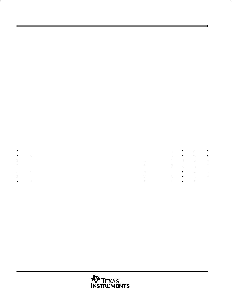
D OR P PACKAGE |
|||||
D High Slew Rate . . . 13 V/ s |
|
|
(TOP VIEW) |
|
|
|
|
|
|
|
|
|
|
D Fast Settling Time . . . 1.1 s to 0.1% |
1OUT |
|
1 |
8 |
|
VCC+ |
|
|
|||||
|
1IN± |
|
|
|
|
|
D Wide-Range Single-Supply |
|
2 |
7 |
|
2OUT |
|
Operation . . . 4 V to 36 V |
1IN+ |
|
3 |
6 |
|
2IN± |
|
|
|||||
D Wide Input Common-Mode Range Includes |
VCC±/GND |
|
4 |
5 |
|
2IN+ |
|
|
|||||
|
|
|
|
|
||
Ground (VCC±) |
|
|
|
|
|
|
|
|
|
|
|
|
|
D D
Low Total Harmonic Distortion . . . 0.02%
Large-Capacitance Drive
Capability . . . 10,000 pF
DOutput Short-Circuit Protection
description
Quality, low-cost, bipolar fabrication with innovative design concepts are employed for the TL3472 operational amplifier. This device offers 4 MHz of gain-bandwidth product, 13-V/ s slew rate, and fast settling time, without the use of JFET device technology. Although the TL3472 can be operated from split supplies, it is particularly suited for single-supply operation because the common-mode input voltage range includes ground potential (VCC±). With a Darlington transistor input stage, this device exhibits high input resistance, low input offset voltage, and high gain. The all-npn output stage, characterized by no dead-band crossover distortion and large output voltage swing, provides high-capacitance drive capability, excellent phase and gain margins, low open-loop high-frequency output impedance, and symmetrical source/sink ac frequency response. This low-cost amplifier is an alternative to the MC33072 and the MC34072 operational amplifiers.
The TL3472C is characterized for operation from 0°C to 70°C. The TL3472I is characterized for operation from ±40°C to 105°C.
AVAILABLE OPTIONS
|
PACKAGED DEVICES |
||
|
|
|
|
TA |
SMALL |
PLASTIC |
|
OUTLINE |
DUAL-IN-LINE |
||
|
|||
|
(D) |
(P) |
|
|
|
|
|
0°C to 70°C |
TL3472CD |
TL3472CP |
|
|
|
|
|
±40°C to 105°C |
TL3472ID |
TL3472IP |
|
|
|
|
|
D package is available taped and reeled. Add the suffix
R to device type (e.g., TL3472CDR).
Please be aware that an important notice concerning availability, standard warranty, and use in critical applications of Texas Instruments semiconductor products and disclaimers thereto appears at the end of this data sheet.
PRODUCTION DATA information is current as of publication date. Products conform to specifications per the terms of Texas Instruments standard warranty. Production processing does not necessarily include testing of all parameters.
Copyright 2000, Texas Instruments Incorporated
POST OFFICE BOX 655303 •DALLAS, TEXAS 75265 |
1 |
TL3472
HIGH-SLEW-RATE, SINGLE-SUPPLY OPERATIONAL AMPLIFIER
SLOS200E ± OCTOBER 1997 ± REVISED FEBRUARY 2000
absolute maximum ratings over operating free-air temperature range (unless otherwise noted)²
Supply voltage (see Note 1): VCC+ . . . . . . . . . . . . . . . . . . . . . . . . . . . . . . . . . . . . . . . . . . . . . . . . . |
. . . . . . . . . 18 V |
VCC± . . . . . . . . . . . . . . . . . . . . . . . . . . . . . . . . . . . . . . . . . . . . . . . . . |
. . . . . . . . ±18 V |
Differential input voltage, VID (see Note 2) . . . . . . . . . . . . . . . . . . . . . . . . . . . . . . . . . . . . . . . . . . . |
. . . . . . . . ±36 V |
Input voltage, VI (any input) . . . . . . . . . . . . . . . . . . . . . . . . . . . . . . . . . . . . . . . . . . . . . . . . . . . . . . . . |
. . . . . . . . VCC± |
Input current, II (each input) . . . . . . . . . . . . . . . . . . . . . . . . . . . . . . . . . . . . . . . . . . . . . . . . . . . . . . . . |
. . . . . . . ±1 mA |
Output current, IO . . . . . . . . . . . . . . . . . . . . . . . . . . . . . . . . . . . . . . . . . . . . . . . . . . . . . . . . . . . . . . . . . |
. . . . . . ±80 mA |
Total current into VCC+ . . . . . . . . . . . . . . . . . . . . . . . . . . . . . . . . . . . . . . . . . . . . . . . . . . . . . . . . . . . . |
. . . . . . . 80 mA |
Total current out of VCC± . . . . . . . . . . . . . . . . . . . . . . . . . . . . . . . . . . . . . . . . . . . . . . . . . . . . . . . . . . . |
. . . . . . . 80 mA |
Duration of short-circuit current at (or below) 25°C (see Note 3) . . . . . . . . . . . . . . . . . . . . . . . . . |
. . . . . Unlimited |
Package thermal impedance, θJA (see Notes 4 and 5): D package . . . . . . . . . . . . . . . . . . . . . . |
. . . . . . 97°C/W |
P package . . . . . . . . . . . . . . . . . . . . . . |
. . . . . . 85°C/W |
Lead temperature 1.6 mm (1/16 inch) from case for 10 seconds . . . . . . . . . . . . . . . . . . . . . . . . |
. . . . . . . 260°C |
Storage temperature range, Tstg . . . . . . . . . . . . . . . . . . . . . . . . . . . . . . . . . . . . . . . . . . . . . . . . . . . |
±65°C to 150°C |
² Stresses beyond those listed under ªabsolute maximum ratingsº may cause permanent damage to the device. These are stress ratings only, and functional operation of the device at these or any other conditions beyond those indicated under ªrecommended operating conditionsº is not implied. Exposure to absolute-maximum-rated conditions for extended periods may affect device reliability.
NOTES: 1. All voltage values, except differential voltages, are with respect to the midpoint between VCC+ and VCC±.
2.Differential voltages are at the noninverting input with respect to the inverting input. Excessive input current can flow when the input is less than VCC± ± 0.3 V.
3.The output can be shorted to either supply. Temperature and/or supply voltages must be limited to ensure that the maximum dissipation rating is not exceeded.
4.Maximum power dissipation is a function of TJ(max), θJA, and TA. The maximum allowable power dissipation at any allowable ambient temperature is PD = (TJ(max) ± TA)/θJA. Operating at the absolute maximum TJ of 150°C can impact reliability.
5.The package thermal impedance is calculated in accordance with JESD 51.
recommended operating conditions
|
|
|
|
MIN |
MAX |
UNIT |
|
|
|
|
|
|
|
|
|
VCC± |
Supply voltage |
|
4 |
36 |
V |
||
VIC |
Common-mode input voltage |
VCC = 5 V |
0 |
2.8 |
V |
||
VCC± = |
±15 V |
±15 |
12.8 |
||||
|
|
|
|||||
TA |
Operating free-air temperature |
TL3472C |
0 |
70 |
°C |
||
|
|
|
|
||||
TL3472I |
|
±40 |
105 |
||||
|
|
|
|
||||
|
|
|
|
|
|
|
|
2 |
POST OFFICE BOX 655303 •DALLAS, TEXAS 75265 |
 Loading...