


TLE2027AIP
Texas Instruments TLE2027AIP, TLE2027AID, TLE2027ACP, TLE2027ACD, TLE2037AMD Datasheet
...
TLE2027, TLE2037, TLE2027A, TLE2037A, TLE2027Y, TLE2037Y
EXCALIBUR LOW-NOISE HIGH-SPEED
PRECISION OPERATIONAL AMPLIFIERS
SLOS192 – FEBRUARY 1997
1
POST OFFICE BOX 655303 • DALLAS, TEXAS 75265
D
Outstanding Combination of dc Precision
and AC Performance:
Unity-Gain Bandwidth...15 MHz Typ
V
n
3.3 nV/√Hz at f = 10 Hz Typ,. . . .
2.5 nV/√Hz at f = 1 kHz Typ
V
IO
25 µV Max. . . .
A
VD
45 V/µV Typ With RL = 2 kΩ,. . .
19 V/µV Typ With RL = 600 Ω
D
Available in Standard-Pinout Small-Outline
Package
D
Output Features Saturation Recovery
Circuitry
D
Macromodels and Statistical information
description
The TLE20x7 and TLE20x7A contain innovative
circuit design expertise and high-quality process
control techniques to produce a level of ac
performance and dc precision previously unavailable in single operational amplifiers. Manufactured using Texas Instruments state-of-the-art
Excalibur process, these devices allow upgrades
to systems that use lower-precision devices.
In the area of dc precision, the TLE20x7 and
TLE20x7A offer maximum offset voltages of
100 µV and 25 µV, respectively, common-mode
rejection ratio of 131 dB (typ), supply voltage
rejection ratio of 144 dB (typ), and dc gain of
45 V/µV (typ).
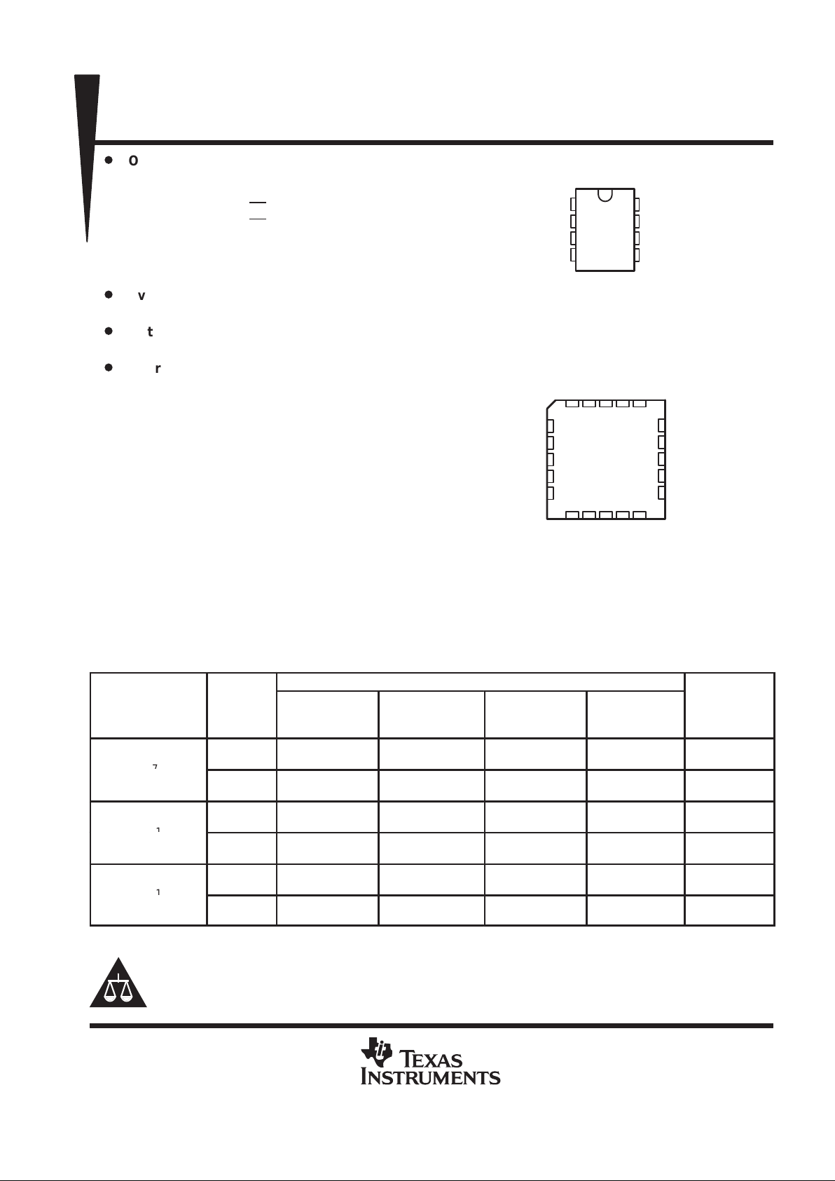
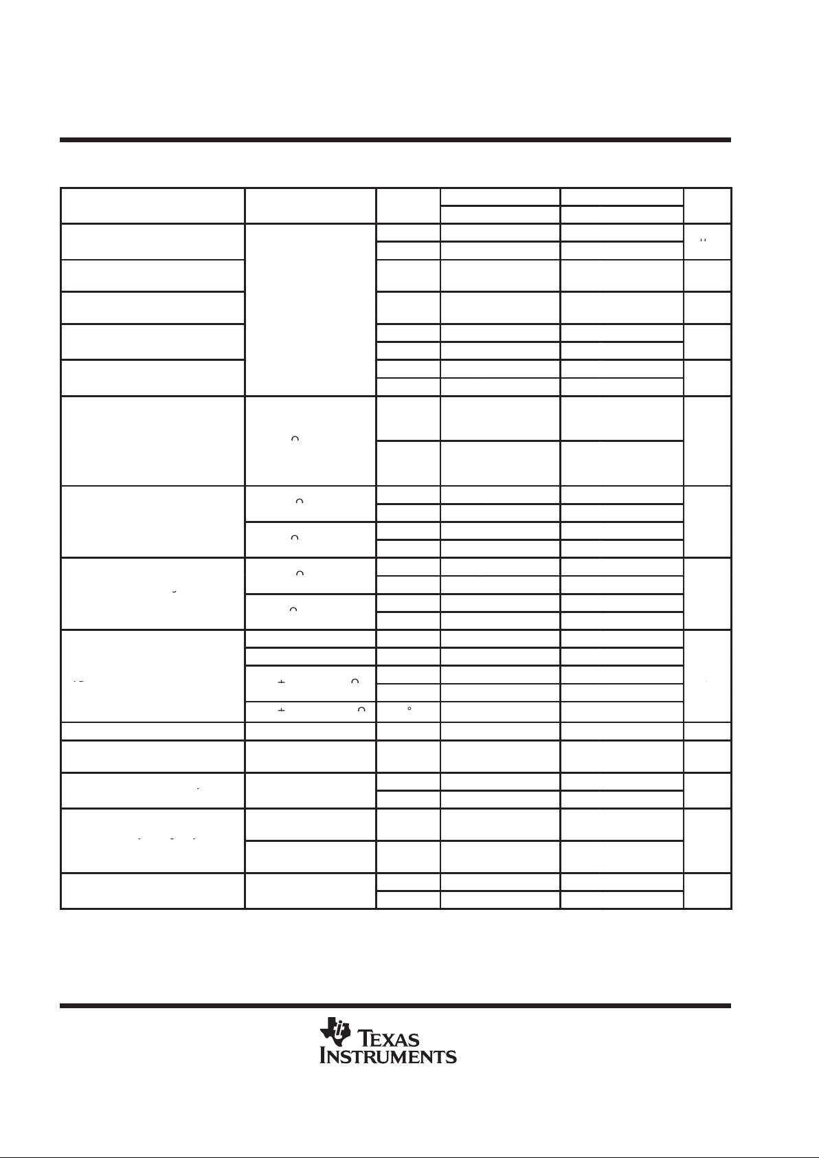
AVAILABLE OPTIONS
PACKAGED DEVICES
T
A
VIOmax AT
25
°C
SMALL
OUTLINE
†
(D)
CHIP
CARRIER
(FK)
CERAMIC
DIP
(JG)
PLASTIC
DIP
(P)
CHIP
FORM
‡
(Y)
25 µV
TLE2027ACD
TLE2037ACD
—
—
—
—
TLE2027ACP
TLE2037ACP
TLE2027Y
TLE2037Y
0°C to 70°C
100 µV
TLE2027CD
TLE2037CD
—
—
—
—
TLE2027CP
TLE2037CP
TLE2027Y
TLE2037Y
25 µV
TLE2027AID
TLE2037AID
—
—
—
—
TLE2027AIP
TLE2037AIP
—
–
40°C to 105°C
100 µV
TLE2027ID
TLE2037ID
—
—
—
—
TLE2027IP
TLE2037IP
—
25 µV
TLE2027AMD
TLE2037AMD
TLE2027AMFK
TLE2037AMFK
TLE2027AMJG
TLE2037AMJG
TLE2027AMP
TLE2037AMP
—
–
55 C to 125 C
100 µV
TLE2027MD
TLE2037MD
TLE2027MFK
TLE2037MFK
TLE2027MJG
TLE2037MJG
TLE2027MP
TLE2037MP
—
†
The D packages are available taped and reeled. Add R suffix to device type (e.g., TLE2027ACDR).
‡
Chip forms are tested at 25°C only.
Copyright 1997, Texas Instruments Incorporated
PRODUCTION DATA information is current as of publication date.
Products conform to specifications per the terms of Texas Instruments
standard warranty. Production processing does not necessarily include
testing of all parameters.
Please be aware that an important notice concerning availability, standard warranty, and use in critical applications of
Texas Instruments semiconductor products and disclaimers thereto appears at the end of this data sheet.
1
2
3
4
8
7
6
5
OFFSET N1
IN –
IN +
V
CC –
OFFSET N2
V
CC +
OUT
NC
D, JG, OR P PACKAGE
(TOP VIEW)
3 2 1 20 19
910111213
4
5
6
7
8
18
17
16
15
14
NC
V
CC+
NC
OUT
NC
NC
IN–
NC
IN+
NC
FK PACKAGE
(TOP VIEW)
NC
OFFSET N1
NCNCNC
NC
NC
NC
OFFSET N2
CC –
V

TLE2027, TLE2037, TLE2027A, TLE2037A, TLE2027Y, TLE2037Y
EXCALIBUR LOW-NOISE HIGH-SPEED
PRECISION OPERATIONAL AMPLIFIERS
SLOS192 – FEBRUARY 1997
2
POST OFFICE BOX 655303 • DALLAS, TEXAS 75265
description (continued)
The ac performance of the TLE2027 and TLE2037 is highlighted by a typical unity-gain bandwidth specification
of 15 MHz, 55° of phase margin, and noise voltage specifications of 3.3 nV/√Hz
and 2.5 nV/√Hz at frequencies
of 10 Hz and 1 kHz respectively . The TLE2037 and TLE2037A have been decompensated for faster slew rate
(–7.5 V/µs, typical) and wider bandwidth (50 MHz). To ensure stability, the TLE2037 and TLE2037A should be
operated with a closed-loop gain of 5 or greater.
Both the TLE20x7 and TLE20x7A are available in a wide variety of packages, including the industry-standard
8-pin small-outline version for high-density system applications. The C-suffix devices are characterized for
operation from 0°C to 70°C. The I-suffix devices are characterized for operation from – 40°C to 105°C. The
M-suffix devices are characterized for operation over the full military temperature range of –55°C to 125°C.
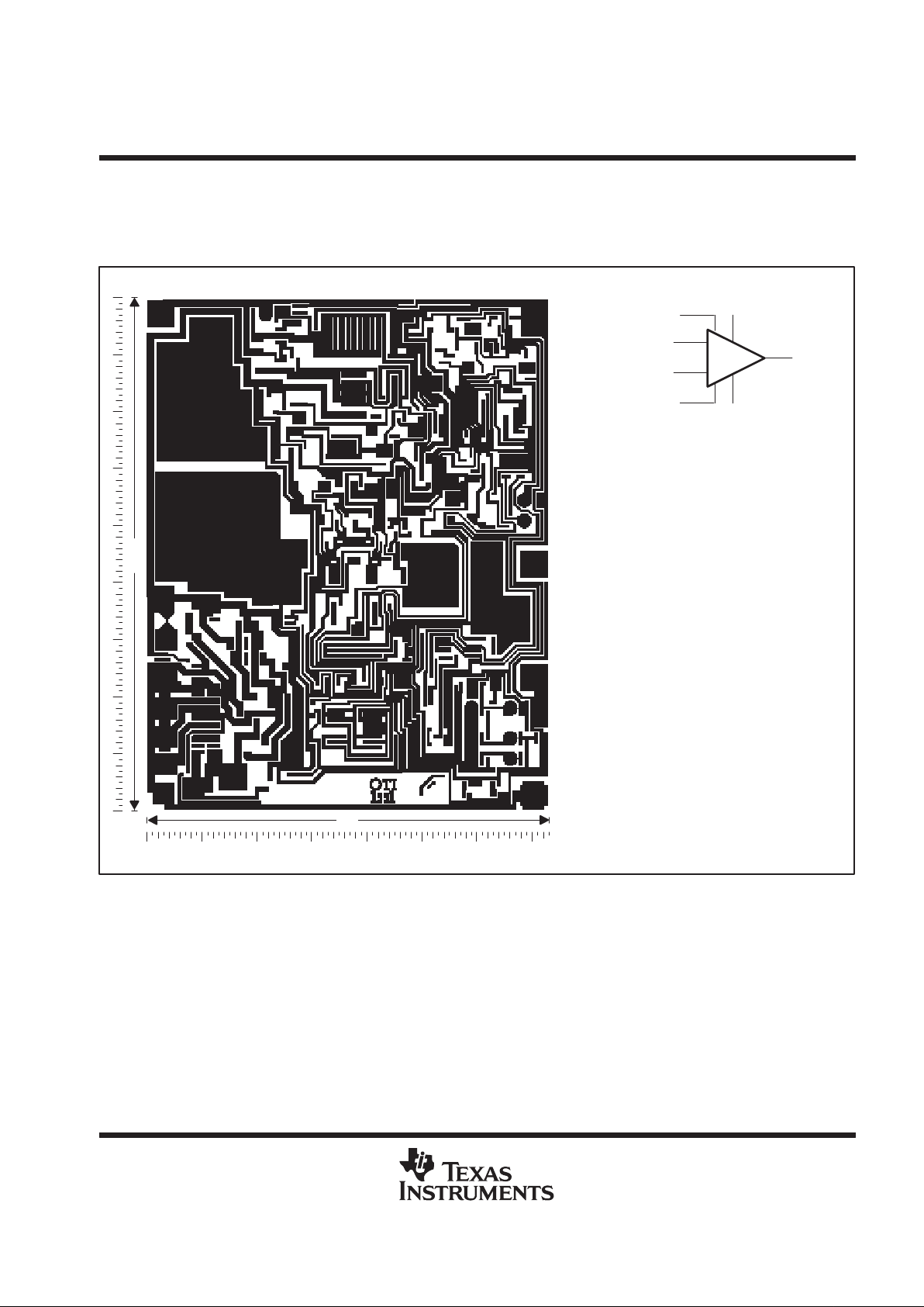
symbol
OUT
OFFSET N2
IN –
IN +
OFFSET N1
–
+
TLE2027, TLE2037, TLE2027A, TLE2037A, TLE2027Y, TLE2037Y
EXCALIBUR LOW-NOISE HIGH-SPEED
PRECISION OPERATIONAL AMPLIFIERS
SLOS192 – FEBRUARY 1997
3
POST OFFICE BOX 655303 • DALLAS, TEXAS 75265
TLE202xY chip information
This chip, when properly assembled, displays characteristics similar to the TLE202xC. Thermal compression
or ultrasonic bonding may be used on the doped-aluminum bonding pads. The chip may be mounted with
conductive epoxy or a gold-silicon preform.
BONDING PAD ASSIGNMENTS
CHIP THICKNESS: 15 MILS TYPICAL
BONDING PADS: 4 × 4 MILS MINIMUM
TJmax = 150°C
TOLERANCES ARE ±10%.
ALL DIMENSIONS ARE IN MILS.
PIN (4) IS INTERNALLY CONNECTED
TO BACKSIDE OF CHIP.
(1) (2) (3)
(4)
(5)
(6)
(7)(8)
90
73
(1)
(2)
(3)
(4)
(6)
(7)
(8)
+
–
OUT
IN+
IN–
V
CC+
V
CC–
OFFSET N1
OFFSET N2
(1)
(3)
(2)
(8)
(7)
(4)
(6)
TLE2027, TLE2037, TLE2027A, TLE2037A, TLE2027Y, TLE2037Y
SLOS192 – FEBRUARY 1997
Template Release Date: 7–11–94
EXCALIBUR LOW-NOISE HIGH-SPEED
PRECISION OPERATIONAL AMPLIFIERS
4
POST OFFICE BOX 655303 DALLAS, TEXAS 75265
•
equivalent schematic
IN –
IN +
R24 R26
Q57
Q56
Q55
Q60
OUT
Q62
Q59
Q61
Q58
R25
Q48
Q54
Q53
Q52
Q49
Q50
R23
R22
R21
R20
Q46
Q42
R19
Q47
Q44
Q43
Q40
Q45
Q41
Q39
Q38
Q37
Q35
R15
Q36
R16
R17
C4
C3
R13
Q34
Q33
Q32
R9
Q27
Q30
R8 R11
Q25 Q28
C2
Q31
Q26 Q29
R18R14R12R10R7
Q19
C1
Q24Q23
Q20
R6
R3
Q21
Q22
Q16
Q15
Q18
R5
R4
Q13
Q14
Q17
R2
R1
OFFSET N2
OFFSET N1
Q12
Q10
Q9
Q11
Q8
Q7
Q5
Q6
Q4
Q1
Q3
Q2
Q51
CC
V
CC+
V
–
ACTUAL DEVICE COMPONENT COUNT
COMPONENT TLE2027 TLE2037
Transistors 61 61
Resistors 26 26
epiFET 1 1
Capacitors 4 4
TLE2027, TLE2037, TLE2027A, TLE2037A, TLE2027Y, TLE2037Y
EXCALIBUR LOW-NOISE HIGH-SPEED
PRECISION OPERATIONAL AMPLIFIERS
SLOS192 – FEBRUARY 1997
6–5
POST OFFICE BOX 655303 • DALLAS, TEXAS 75265
absolute maximum ratings over operating free-air temperature range (unless otherwise noted)
†
Supply voltage, V
CC+
(see Note 1) 19 V. . . . . . . . . . . . . . . . . . . . . . . . . . . . . . . . . . . . . . . . . . . . . . . . . . . . . . . . .
Supply voltage, V
CC–
– 19 V. . . . . . . . . . . . . . . . . . . . . . . . . . . . . . . . . . . . . . . . . . . . . . . . . . . . . . . . . . . . . . . . . . . .
Differential input voltage, V
ID
(see Note 2) ±1.2 V. . . . . . . . . . . . . . . . . . . . . . . . . . . . . . . . . . . . . . . . . . . . . . . . . .
Input voltage range, V
I
(any input) V
CC±
. . . . . . . . . . . . . . . . . . . . . . . . . . . . . . . . . . . . . . . . . . . . . . . . . . . . . . . . .
Input current, I
I
(each Input) ±1 mA. . . . . . . . . . . . . . . . . . . . . . . . . . . . . . . . . . . . . . . . . . . . . . . . . . . . . . . . . . . . . .
Output current, I
O
± 50 mA. . . . . . . . . . . . . . . . . . . . . . . . . . . . . . . . . . . . . . . . . . . . . . . . . . . . . . . . . . . . . . . . . . . . .
Total current into V
CC+
50 mA. . . . . . . . . . . . . . . . . . . . . . . . . . . . . . . . . . . . . . . . . . . . . . . . . . . . . . . . . . . . . . . . . . .
Total current out of V
CC–
50 mA. . . . . . . . . . . . . . . . . . . . . . . . . . . . . . . . . . . . . . . . . . . . . . . . . . . . . . . . . . . . . . . . .
Duration of short-circuit current at (or below) 25°C (see Note 3) unlimited. . . . . . . . . . . . . . . . . . . . . . . . . . . .
Continuous total power dissipation See Dissipation Rating Table. . . . . . . . . . . . . . . . . . . . . . . . . . . . . . . . . . . . .
Operating free-air temperature range, T
A
: C suffix 0°C to 70°C. . . . . . . . . . . . . . . . . . . . . . . . . . . . . . . . . . . . . .
I suffix – 40°C to 105°C . . . . . . . . . . . . . . . . . . . . . . . . . . . . . . . . . .
M suffix – 55°C to 125°C. . . . . . . . . . . . . . . . . . . . . . . . . . . . . . . . . .
Storage temperature range, T
stg
–65°C to 150°C. . . . . . . . . . . . . . . . . . . . . . . . . . . . . . . . . . . . . . . . . . . . . . . . . .
Case temperature for 60 seconds, T
C
: FK package 260°C. . . . . . . . . . . . . . . . . . . . . . . . . . . . . . . . . . . . . . . . . .
Lead temperature 1,6 mm (1/16 inch) from case for 10 seconds: D or P package 260°C. . . . . . . . . . . . . . . .
Lead temperature 1,6 mm (1/16 inch) from case for 60 seconds: JG package 300°C. . . . . . . . . . . . . . . . . . .
†
Stresses beyond those listed under “absolute maximum ratings” may cause permanent damage to the device. These are stress ratings only, and
functional operation of the device at these or any other conditions beyond those indicated under “recommended operating conditions” is not
implied. Exposure to absolute-maximum-rated conditions for extended periods may affect device reliability.
NOTES: 1. All voltage values, except differential voltages, are with respect to the midpoint between V
CC +
and V
CC –
.
2. Differential voltages are at IN+ with respect to IN–. Excessive current flows if a differential input voltage in excess of approximately
±1.2 V is applied between the inputs unless some limiting resistance is used.
3. The output may be shorted to either supply. Temperature and/or supply voltages must be limited to ensure that the maximum
dissipation rating is not exceeded.
DISSIPATION RATING TABLE
PACKAGE
TA ≤ 25°C
POWER RATING
DERATING FACTOR
ABOVE TA = 25°C
TA = 70°C
POWER RATING
TA = 105°C
POWER RATING
TA = 125°C
POWER RATING
D 725 mW 5.8 mW/°C 464 mW 261 mW 145 mW
FK 1375 mW 11.0 mW/°C 880 mW 495 mW 275 mW
JG 1050 mW 8.4 mW/°C 672 mW 378 mW 210 mW
P 1000 mW 8.0 mW/°C 640 mW 360 mW 200 mW
recommended operating conditions
C SUFFIX I SUFFIX M SUFFIX
MIN MAX MIN MAX MIN MAX
UNIT
Supply voltage, V
CC±
±4 ± 19 ±4 ±19 ±4 ±19 V
p
TA = 25°C –11 11 –11 11 –11 11
Common-mode input voltage, V
IC
TA = Full range
‡
–10.5 10.5 –10.4 10.4 –10.2 10.2
V
Operating free-air temperature, T
A
0 70 –40 105 –55 125 °C
‡
Full range is 0°C to 70°C for C-suffix devices, –40°C to 105°C for I-suffix devices, and –55°C to 125°C for M-suffix devices.
TLE2027, TLE2037, TLE2027A, TLE2037A, TLE2027Y, TLE2037Y
EXCALIBUR LOW-NOISE HIGH-SPEED
PRECISION OPERATIONAL AMPLIFIERS
SLOS192 – FEBRUARY 1997
6–6
POST OFFICE BOX 655303 • DALLAS, TEXAS 75265
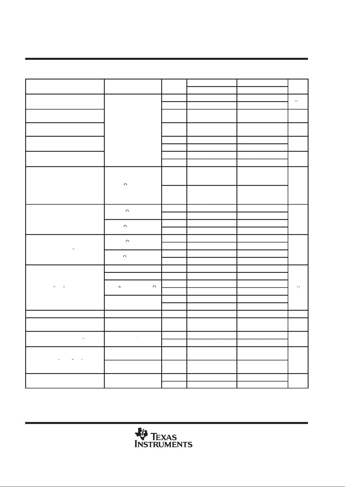
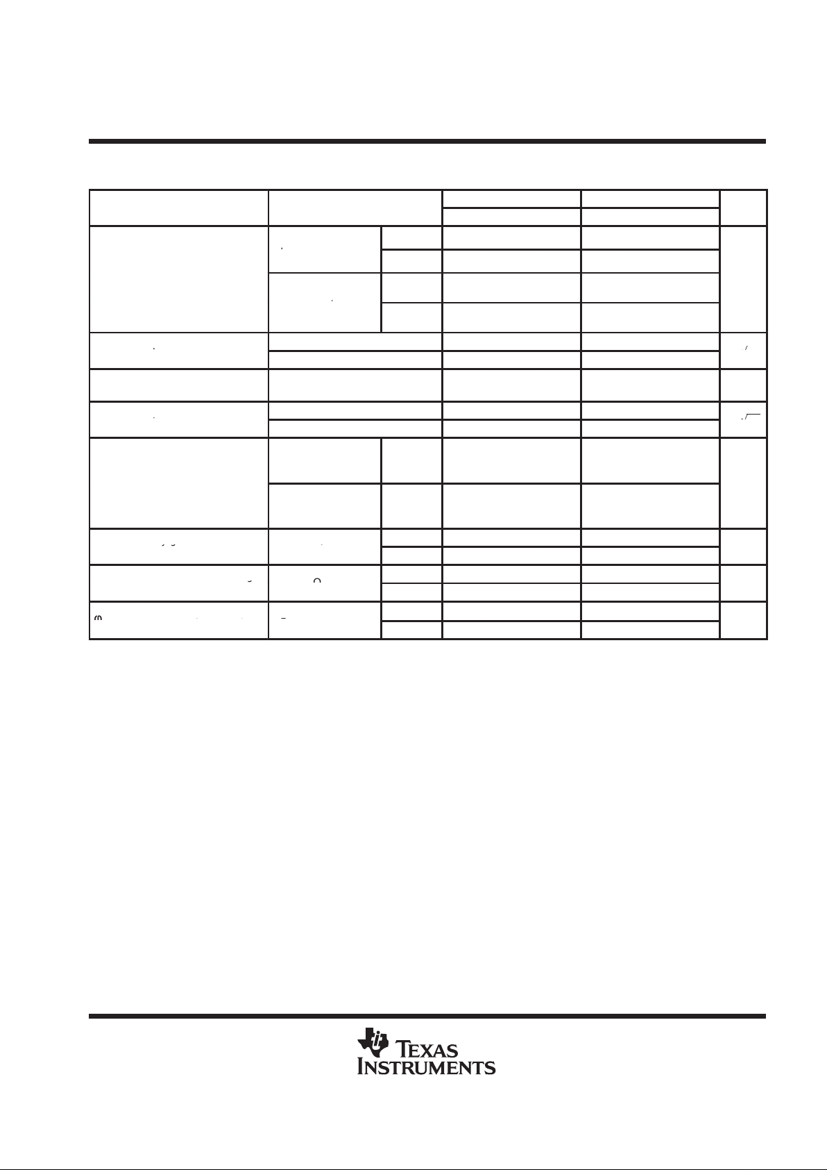
TLE20x7C electrical characteristics at specified free-air temperature, V
CC
±
= ±15 V (unless
otherwise noted)
TLE20x7C TLE20x7AC
PARAMETER
TEST CONDITIONS
T
A
†
MIN TYP MAX MIN TYP MAX
UNIT
p
25°C 20 100 10 25
VIOInput offset voltage
Full range 145 70
µ
V
α
VIO
T emperature coef ficient of
input offset voltage
Full range 0.4 1 0.2 1 µV/°C
Input offset voltage
long-term drift (see Note 4)
VIC = 0, RS = 50 Ω
25°C 0.006 1 0.006 1 µV/mo
p
25°C 6 90 6 90
IIOInput offset current
Full range 150 150
nA
p
25°C 15 90 15 90
IIBInput bias current
Full range 150 150
nA
Common-mode input
25°C
–11
to
11
–13
to
13
–11
to
11
–13
to
13
V
ICR
voltage range
R
S
= 50
Ω
Full range
–10.5
to
10.5
–10.5
to
10.5
V
25°C 10.5 12.9 10.5 12.9
Maximum positive peak
R
L
=
600 Ω
Full range 10 10
V
OM +
output voltage swing
25°C 12
13.2
12 13.2
V R
L
=
2 kΩ
Full range 11 11
25°C –10.5 –13 –10.5 –13
Maximum negative peak
R
L
=
600 Ω
Full range –10 –10
V
OM –
g
output voltage swing
25°C –12 –13.5 –12 –13.5
V
R
L
= 2
kΩ
Full range –11 –11
VO = ±11 V, RL = 2 kΩ 25°C 5 45 10 45
VO = ±10 V, RL = 2 kΩ Full range 2 4
Large-signal differential
25°C 3.5 38 8 38
A
VD
gg
voltage amplification
V
O
=
±10 V, R
L
= 1
kΩ
Full range 1 2.5
V/µV
V
= ±10 V ,
25°C 2 19 5 19
O
,
RL = 600 Ω
Full range 0.5 2
C
i
Input capacitance 25°C 8 8 pF
z
o
Open-loop output
impedance
IO = 0 25°C 50 50
Ω
Common-mode rejection V
= V
min,
25°C 100 131 117 131
CMRR
j
ratio
IC ICR
,
RS = 50 Ω
Full range 98 114
dB
Supply-voltage rejection
V
CC±
= ±4 V to ±18 V,
RS = 50 Ω
25°C 94 144 110 144
k
SVR
ygj
ratio (∆V
CC
±
/∆V
IO
)
V
CC±
= ±4 V to ±18 V,
RS = 50 Ω
Full range 92 106
dB
pp
25°C 3.8 5.3 3.8 5.3
ICCSupply current
V
O
= 0,
No load
Full range 5.6 5.6
mA
†
Full range is 0°C to 70°C.
NOTE 4: Typical values are based on the input offset voltage shift observed through 168 hours of operating life test at TA = 150°C extrapolated
to TA = 25°C using the Arrhenius equation and assuming an activation energy of 0.96 eV .
TLE2027, TLE2037, TLE2027A, TLE2037A, TLE2027Y, TLE2037Y
EXCALIBUR LOW-NOISE HIGH-SPEED
PRECISION OPERATIONAL AMPLIFIERS
SLOS192 – FEBRUARY 1997
6–7
POST OFFICE BOX 655303 • DALLAS, TEXAS 75265
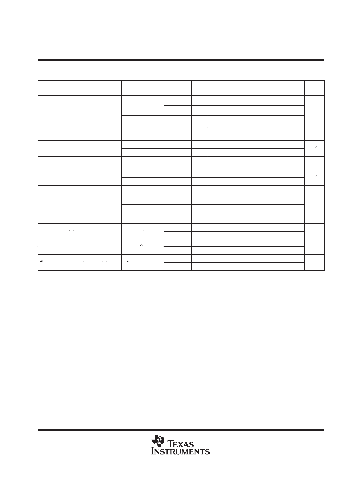
TLE20x7C operating characteristics at specified free-air temperature, V
CC ±
= ±15 V, TA = 25°C
(unless otherwise specified)
TLE20x7C TLE20x7AC
PARAMETER
TEST CONDITIONS
MIN TYP MAX MIN TYP MAX
UNIT
RL = 2 kΩ,
p
TLE2027 1.7 2.8 1.7 2.8
C
L
=
100 pF
,
See Figure 1
TLE2037 6 7.5 6 7.5
SR Slew rate at unity gain
RL = 2 kΩ,
C
= 100 pF,
TLE2027 1.2 1.2
V/µs
L
,
TA = 0°C to 70°C,
See Figure 1
TLE2037 5 5
Equivalent input noise volt-
RS = 20 Ω, f = 10 Hz 3.3 8 3.3 4.5
V
n
q
age (see Figure 2)
RS = 20 Ω, f = 1 kHz
2.5 4.5 2.5 3.8
n
V/√H
z
V
N(PP)
Peak-to-peak equivalent input noise voltage
f = 0.1 Hz to 10 Hz 50 250 50 130 nV
Equivalent input noise cur-
f = 10 Hz 1.5 4 1.5 4
I
n
q
rent
f = 1 kHz
0.4 0.6 0.4 0.6
p
A/√H
z
VO = +10 V ,
AVD = 1,
See Note 5
TLE2027 <0.002% <0.002%
THD
Total harmonic distortion
VO = +10 V ,
AVD = 5,
See Note 5
TLE2037 <0.002% <0.002%
Unity-gain bandwidth R
= 2 kΩ,
TLE2027 7 13 9 13
B
1
yg
(see Figure 3)
L
,
CL = 100 pF
TLE2037 35 50 35 50
MH
z
Maximum output-swing
TLE2027 30 30
B
OM
g
bandwidth
R
L
= 2
kΩ
TLE2037 80 80
kH
z
Phase margin at unity gain RL = 2 kΩ,
TLE2027 55° 55°
φ
m
gyg
(see Figure 3)
L
CL = 100 pF
TLE2037 50° 50°
NOTE 5: Measured distortion of the source used in the analysis was 0.002%.
TLE2027, TLE2037, TLE2027A, TLE2037A, TLE2027Y, TLE2037Y
EXCALIBUR LOW-NOISE HIGH-SPEED
PRECISION OPERATIONAL AMPLIFIERS
SLOS192 – FEBRUARY 1997
6–8
POST OFFICE BOX 655303 • DALLAS, TEXAS 75265
TLE20x7I electrical characteristics at specified free-air temperature, V
CC±
= ±15 V (unless
otherwise noted)
TLE20x7I TLE20x7AI
PARAMETER
TEST CONDITIONS
T
A
†
MIN TYP MAX MIN TYP MAX
UNIT
p
25°C 20 100 10 25
VIOInput offset voltage
Full range 180 105
µ
V
α
VIO
T emperature coef ficient of
input offset voltage
Full range 0.4 1 0.2 1 µV/°C
Input offset voltage
long-term drift (see Note 4)
VIC = 0, RS = 50 Ω
25°C 0.006 1 0.006 1 µV/mo
p
25°C 6 90 6 90
IIOInput offset current
Full range 150 150
nA
p
25°C 15 90 15 90
IIBInput bias current
Full range 150 150
nA
Common-mode input
25°C
–11
to
11
–13
to
13
–11
to
11
–13
to
13
V
ICR
voltage range
R
S
= 50
Ω
Full range
–10.4
to
10.4
–10.4
to
10.4
V
25°C 10.5 12.9 10.5 12.9
Maximum positive peak
R
L
=
600 Ω
Full range 10 10
V
OM +
output voltage swing
25°C 12
13.2
12 13.2
V R
L
=
2 kΩ
Full range 11 11
25°C –10.5 –13 –10.5 –13
Maximum negative peak
R
L
=
600 Ω
Full range –10 –10
V
OM –
g
output voltage swing
25°C –12 –13.5 –12 –13.5
V
R
L
= 2
kΩ
Full range –11 –11
VO = ±11 V, RL = 2 kΩ 25°C 5 45 10 45
VO = ±10 V, RL = 2 kΩ Full range 2 3.5
Large-signal differential
25°C 3.5 38 8 38
A
VD
gg
voltage amplification
V
O
=
±10 V, R
L
= 1
kΩ
Full range 1 2.2
V/µV
25°C 2 19 5 19
V
O
=
±10 V, R
L
=
600 Ω
Full range 0.5 1.1
C
i
Input capacitance 25°C 8 8 pF
z
o
Open-loop output
impedance
IO = 0 25°C 50 50
Ω
Common-mode rejection V
= V
min,
25°C 100 131 117 131
CMRR
j
ratio
IC ICR
,
RS = 50 Ω
Full range 96 113
dB
Supply-voltage rejection
V
CC±
= ±4 V to ±18 V,
RS = 50 Ω
25°C 94 144 110 144
k
SVR
ygj
ratio (∆V
CC
±
/∆VIO)
V
CC±
= ±4 V to ±18 V,
RS = 50 Ω
Full range 90 105
dB
pp
25°C 3.8 5.3 3.8 5.3
ICCSupply current
V
O
= 0,
No load
Full range 5.6 5.6
mA
†
Full range is – 40°C to 105°C.
NOTE 4: Typical values are based on the input offset voltage shift observed through 168 hours of operating life test at TA = 150°C extrapolated
to TA = 25°C using the Arrhenius equation and assuming an activation energy of 0.96 eV .
TLE2027, TLE2037, TLE2027A, TLE2037A, TLE2027Y, TLE2037Y
EXCALIBUR LOW-NOISE HIGH-SPEED
PRECISION OPERATIONAL AMPLIFIERS
SLOS192 – FEBRUARY 1997
6–9
POST OFFICE BOX 655303 • DALLAS, TEXAS 75265
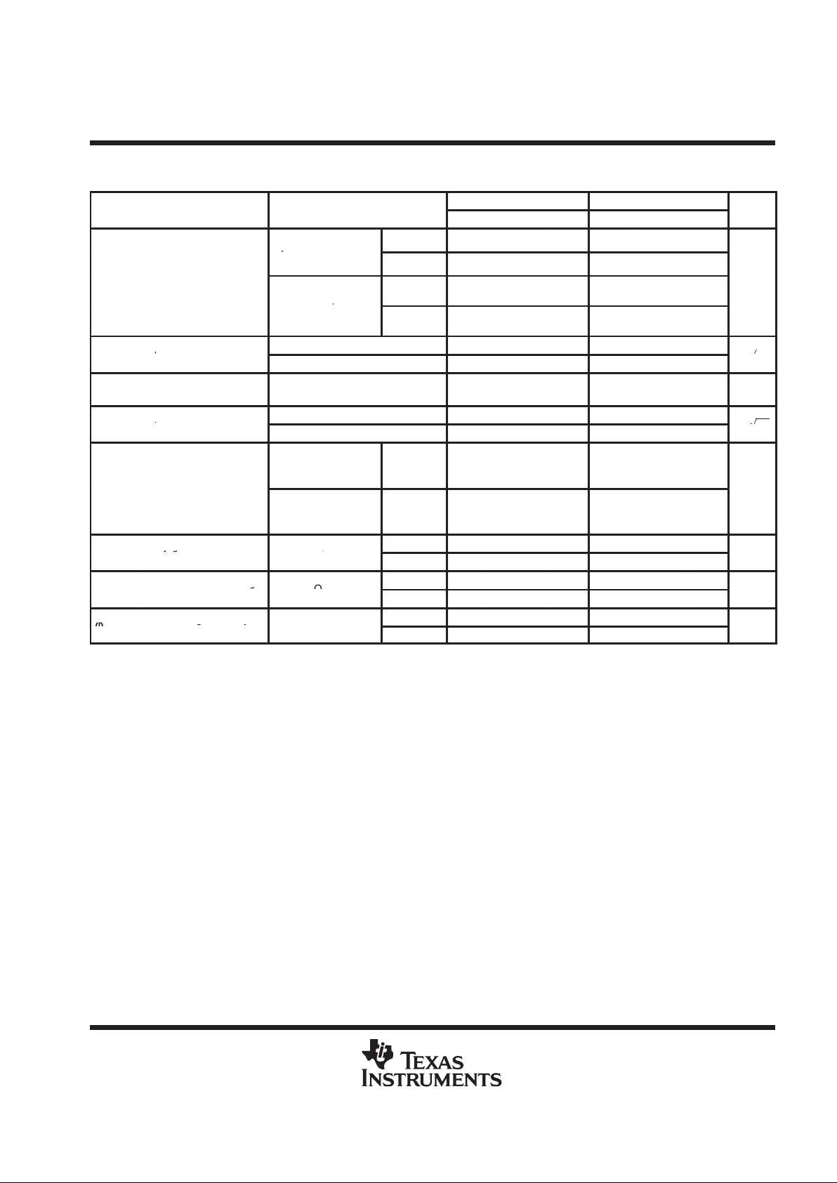
TLE20x7I operating characteristics at specified free-air temperature, V
CC ±
= ±15 V, TA = 25°C
(unless otherwise specified)
TLE20x7I TLE20x7AI
PARAMETER
TEST CONDITIONS
MIN TYP MAX MIN TYP MAX
UNIT
RL = 2 kΩ,
p
TLE2027 1.7 2.8 1.7 2.8
C
L
=
100 pF
,
See Figure 1
TLE2037 6 7.5 6 7.5
SR Slew rate at unity gain
RL = 2 kΩ,
C
= 100 pF,
TLE2027 1.1 1.1
V/µs
L
,
TA = –40°C to 85°C,
See Figure 1
TLE2037 4.7 4.7
Equivalent input noise
RS = 20 Ω, f = 10 Hz 3.3 8 3.3 4.5
V
n
q
voltage (see Figure 2)
RS = 20 Ω, f = 1 kHz
2.5 4.5 2.5 3.8
n
V/√H
z
V
N(PP)
Peak-to-peak equivalent
input noise voltage
f = 0.1 Hz to 10 Hz 50 250 50 130 nV
Equivalent input noise
f = 10 Hz 1.5 4 1.5 4
I
n
q
current
f = 1 kHz
0.4 0.6 0.4 0.6
p
A/√H
z
VO = +10 V ,
AVD = 1,
See Note 5
TLE2027 < 0.002% < 0.002%
THD
Total harmonic distortion
VO = +10 V ,
AVD = 5,
See Note 5
TLE2037 < 0.002% < 0.002%
Unity-gain bandwidth R
= 2 kΩ,
TLE2027 7 13 9 13
B
1
yg
(see Figure 3)
L
,
CL = 100 pF
TLE2037 35 50 35 50
MH
z
Maximum output-swing
TLE2027 30 30
B
OM
g
bandwidth
R
L
= 2
kΩ
TLE2037 80 80
kH
z
Phase margin at unity R
= 2 kΩ,
TLE2027 55° 55°
φ
m
gy
gain (see Figure 3)
L
,
CL = 100 pF
TLE2037 50° 50°
NOTE 5: Measured distortion of the source used in the analysis was 0.002%.
TLE2027, TLE2037, TLE2027A, TLE2037A, TLE2027Y, TLE2037Y
EXCALIBUR LOW-NOISE HIGH-SPEED
PRECISION OPERATIONAL AMPLIFIERS
SLOS192 – FEBRUARY 1997
6–10
POST OFFICE BOX 655303 • DALLAS, TEXAS 75265
TLE20x7M electrical characteristics at specified free-air temperature, V
CC
±
= ±15 V (unless
otherwise noted)
TLE20x7M TLE20x7AM
PARAMETER
TEST CONDITIONS
T
A
†
MIN TYP MAX MIN TYP MAX
UNIT
p
25°C 20 100 10 25
VIOInput offset voltage
Full range 200 105
µ
V
α
VIO
T emperature coef ficient of
input offset voltage
Full range 0.4 1* 0.2 1* µV/°C
Input offset voltage
long-term drift (see Note 4)
VIC = 0, RS = 50 Ω
25°C 0.006 1* 0.006 1* µV/mo
p
25°C 6 90 6 90
IIOInput offset current
Full range 150 150
nA
p
25°C 15 90 15 90
IIBInput bias current
Full range 150 150
nA
Common-mode input
25°C
–11
to
11
–13
to
13
–11
to
11
–13
to
13
V
ICR
voltage range
R
S
= 50
Ω
Full range
–10.3
to
10.3
–10.4
to
10.4
V
25°C 10.5 12.9 10.5 12.9
Maximum positive peak
R
L
=
600 Ω
Full range 10 10
V
OM +
output voltage swing
25°C 12 13.2 12 13.2
V R
L
=
2 kΩ
Full range 11 11
25°C –10.5 –13 –10.5 –13
Maximum negative peak
R
L
=
600 Ω
Full range –10 –10
V
OM –
g
output voltage swing
25°C –12 –13.5 –12 –13.5
V
R
L
= 2
kΩ
Full range –11 –11
VO = ±11 V, RL = 2 kΩ 25°C 5 45 10 45
VO = ±10 V, RL = 2 kΩ Full range 2.5 3.5
A
VD
Large-signal differential
p
25°C 3.5 38 8 38
V/µV
VD
voltage am lification
V
O
=
±10 V, R
L
= 1
kΩ
Full range 1.8 2.2
µ
V
O
=
±10 V, R
L
=
600 Ω
25°C219519
Ci
Input capacitance 25°C 8 8 pF
z
o
Open-loop output
impedance
IO = 0 25°C 50 50
Ω
Common-mode rejection V
= V
min,
25°C 100 131 117 131
CMRR
j
ratio
IC ICR
,
RS = 50 Ω
Full range 96 113
dB
Supply-voltage rejection
V
CC±
= ±4 V to ±18 V,
RS = 50 Ω
25°C 94 144 110 144
k
SVR
ygj
ratio (∆V
CC
±
/∆V
IO
)
V
CC±
= ±4 V to ±18 V,
RS = 50 Ω
Full range 90 105
dB
pp
25°C 3.8 5.3 3.8 5.3
ICCSupply current
V
O
= 0, No
load
Full range 5.6 5.6
mA
* On products compliant to MIL-PRF-38535, this parameter is not production tested.
†
Full range is – 55°C to 125°C.
NOTE 4: Typical values are based on the input offset voltage shift observed through 168 hours of operating life test at TA = 150°C extrapolated
to TA = 25°C using the Arrhenius equation and assuming an activation energy of 0.96 eV .
TLE2027, TLE2037, TLE2027A, TLE2037A, TLE2027Y, TLE2037Y
EXCALIBUR LOW-NOISE HIGH-SPEED
PRECISION OPERATIONAL AMPLIFIERS
SLOS192 – FEBRUARY 1997
6–11
POST OFFICE BOX 655303 • DALLAS, TEXAS 75265
TLE20x7M operating characteristics at specified free-air temperature, V
CC ±
= ±15 V, TA = 25°C
(unless otherwise specified)
TLE20x7M TLE20x7AM
PARAMETER
TEST CONDITIONS
MIN TYP MAX MIN TYP MAX
UNIT
RL = 2 kΩ,
p
TLE2027 1.7 2.8 1.7 2.8
C
L
=
100 pF
,
See Figure 1
TLE2037 6* 7.5 6* 7.5
SR Slew rate at unity gain
RL = 2 kΩ,
C
= 100 pF,
TLE2027 1 1
V/µs
L
,
TA = –55°C to 125°C,
See Figure 1
TLE2037 4.4* 4.4*
Equivalent input noise
RS = 20 Ω, f = 10 Hz 3.3 8* 3.3 4.5*
V
n
q
voltage (see Figure 2)
RS = 20 Ω, f = 1 kHz
2.5 4.5* 2.5 3.8*
n
V/√H
z
V
N(PP)
Peak-to-peak equivalent
input noise voltage
f = 0.1 Hz to 10 Hz 50 250* 50 130* nV
Equivalent input noise
f = 10 Hz 1.5 4* 1.5 4*
I
n
q
current
f = 1 kHz
0.4 0.6* 0.4 0.6*
p
A/√H
z
VO = +10 V ,
AVD = 1,
See Note 5
TLE2027 <0.002% < 0.002%
THD
Total harmonic distortion
VO = +10 V ,
AVD = 5,
See Note 5
TLE2037 <0.002% < 0.002%
Unity-gain bandwidth R
= 2 kΩ,
TLE2027 7* 13 9* 13
B
1
yg
(see Figure 3)
L
,
CL = 100 pF
TLE2037 35 50 35 50
MH
z
Maximum output-swing
TLE2027 30 30
B
OM
g
bandwidth
R
L
= 2
kΩ
TLE2037 80 80
kH
z
Phase margin at unity RL = 2 kΩ,
TLE2027 55° 55°
φ
m
gy
gain (see Figure 3)
L
CL = 100 pF
TLE2037 50° 50°
* On products compliant to MIL-PRF-38535, this parameter is not production tested.
NOTE 5: Measured distortion of the source used in the analysis was 0.002%.
 Loading...