


|
|
DUAL MICROPOWER LinCMOS |
|
|
|
TLC193, TLC393 |
||||
|
|
VOLTAGE COMPARATOR |
||||||||
|
|
|
SLCS115D ± DECEMBER 1986 ± REVISED JANUARY 1999 |
|||||||
|
|
|
|
|
|
|
|
|
|
|
D |
μ |
W Typ at 5 V |
D, JG, P, OR PW PACKAGE |
|||||||
|
Very Low Power . . . 110 |
|
|
(TOP VIEW) |
|
|
||||
D Fast Response Time . . . tPLH = 2.5 μs Typ |
|
|
|
|
||||||
|
|
|
|
|
|
|
|
|||
|
With 5-mV Overdrive |
|
1OUT |
|
1 |
8 |
|
|
VDD |
|
|
|
|
|
|
||||||
D |
Single Supply Operation: |
|
|
|
|
|||||
|
1IN ± |
|
|
|
|
|
||||
|
|
2 |
7 |
|
|
2OUT |
||||
|
TLC393C . . . 3 V to 16 V |
|
|
|
||||||
|
1IN + |
|
3 |
6 |
|
|
2IN ± |
|||
|
|
|
|
|||||||
|
TLC393I . . . 3 V to 16 V |
|
|
|
||||||
|
GND |
|
4 |
5 |
|
|
2IN + |
|||
|
|
|
|
|||||||
|
TLC393Q . . . 4 V to 16 V |
|
|
|
||||||
|
|
|
|
|
|
|
|
|
||
|
|
|
|
|
|
|
|
|
||
|
TLC393M . . . 4 V to 16 V |
|
|
|
|
|
|
|
|
|
|
TLC193M . . . 4 V to 16 V |
|
FK PACKAGE |
|
|
|||||
D |
On-Chip ESD Protection |
|
|
|
(TOP VIEW) |
|
|
|||
description
The TLC193 and TLC393 consist of dual independent micropower voltage comparators designed to operate from a single supply. They are functionally similar to the LM393 but uses one-twentieth the power for similar response times. The open-drain MOS output stage interfaces to a variety of loads and supplies. For a similar device with a push-pull output configuration (see the TLC3702 data sheet).
|
NC |
1OUT |
NC |
DD |
NC |
|
|
V |
|
||||
NC |
3 |
2 |
1 |
20 19 |
|
|
4 |
|
|
|
18 |
NC |
|
1IN ± |
5 |
|
|
|
17 |
|
NC |
6 |
|
|
|
16 |
2OUT |
1IN + |
7 |
|
|
|
15 |
NC |
NC |
8 |
|
|
|
14 |
2IN ± |
|
9 |
10 11 12 13 |
NC |
|||
|
|
|
|
|
|
|
|
NC |
GND |
NC |
2IN+ |
NC |
|
Texas Instruments LinCMOS process offers superior analog performance to standard CMOS processes. Along with the standard CMOS advantages of low power without sacrificing speed, high input impedance, and low bias currents, the LinCMOS process offers extremely stable input offset voltages, even with differential input stresses of several volts. This characteristic makes it possible to build reliable CMOS comparators.
NC ± No internal connection
symbol (each comparator)
IN +
OUT
IN ±
The TLC393C is characterized for operation over the commercial temperature range of TA = 0°C to 70°C. The TLC393I is characterized for operation over the extended industrial temperature range of TA = ±40°C to 85°C. The TLC393Q is characterized for operation over the full automotive temperature range of TA = ±40°C to 125°C. The TLC193M and TLC393M are characterized for operation over the full military temperature range of TA = ±55°C to 125°C.
Please be aware that an important notice concerning availability, standard warranty, and use in critical applications of Texas Instruments semiconductor products and disclaimers thereto appears at the end of this data sheet.
LinCMOS is a trademark of Texas Instruments Incorporated.
PRODUCTION DATA information is current as of publication date. Products conform to specifications per the terms of Texas Instruments standard warranty. Production processing does not necessarily include testing of all parameters.
Copyright 1999, Texas Instruments Incorporated
POST OFFICE BOX 655303 •DALLAS, TEXAS 75265 |
1 |
TLC193, TLC393
DUAL MICROPOWER LinCMOS VOLTAGE COMPARATOR
SLCS115D ± DECEMBER 1986 ± REVISED JANUARY 1999
AVAILABLE OPTIONS
|
VIOmax |
|
|
PACKAGES |
|
|
|
TA |
|
|
|
|
|
||
SMALL OUTLINE |
CHIP CARRIER |
CERAMIC DIP |
PLASTIC DIP |
TSSOP |
|||
at 25°C |
|||||||
|
(D) |
(FK) |
(JG) |
(P) |
(PW) |
||
|
|
||||||
|
|
|
|
|
|
|
|
0°C to 70°C |
5 mV |
TLC393CD |
Ð |
Ð |
TLC393CP |
TLC393CPWLE |
|
|
|
|
|
|
|
|
|
± 40°C to 85°C |
5 mV |
TLC393ID |
Ð |
Ð |
TLC393IP |
TLC393IPWLE |
|
|
|
|
|
|
|
|
|
± 40°C to 125°C |
5 mV |
TLC393QD |
Ð |
Ð |
Ð |
Ð |
|
|
|
|
|
|
|
|
|
± 55°C to 125°C |
5 mV |
TLC393MD |
TLC193MFK |
TLC193MJG |
TLC393MP |
Ð |
|
|
|
|
|
|
|
|
² The D package is available taped and reeled. Add the suffix R to the device type (e.g., TLC393CDR).
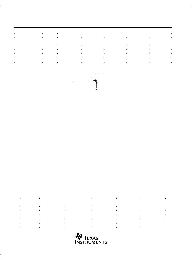
schematic
OUT
OPEN-DRAIN CMOS OUTPUT
absolute maximum ratings over operating free-air temperature range (unless otherwise noted)²
Supply voltage range, VDD (see Note 1) . . . . . . . . . . . . . . . . . . . . . . . . . . . . . . . . . |
. . . . . . . . . . . |
. ± 0.3 V to 18 V |
Differential input voltage, VID (see Note 2) . . . . . . . . . . . . . . . . . . . . . . . . . . . . . . . |
. . . . . . . . . . . . |
. . . . . . . . ±18 V |
Input voltage range, VI . . . . . . . . . . . . . . . . . . . . . . . . . . . . . . . . . . . . . . . . . . . . . . . . . |
. . . . . . . . . . . . |
± 0.3 V to VDD |
Output voltage range, VO . . . . . . . . . . . . . . . . . . . . . . . . . . . . . . . . . . . . . . . . . . . . . . |
. . . . . . . . . . . . |
± 0.3 V to 16 V |
Input current, II . . . . . . . . . . . . . . . . . . . . . . . . . . . . . . . . . . . . . . . . . . . . . . . . . . . . . . . |
. . . . . . . . . . . . |
. . . . . . . ±5 mA |
Output current, IO (each output) . . . . . . . . . . . . . . . . . . . . . . . . . . . . . . . . . . . . . . . . |
. . . . . . . . . . . . |
. . . . . . . 20 mA |
Total supply current into VDD . . . . . . . . . . . . . . . . . . . . . . . . . . . . . . . . . . . . . . . . . . . |
. . . . . . . . . . . . |
. . . . . . . 40 mA |
Total current out of GND . . . . . . . . . . . . . . . . . . . . . . . . . . . . . . . . . . . . . . . . . . . . . . . |
. . . . . . . . . . . . |
. . . . . . . 40 mA |
Continuous total power dissipation . . . . . . . . . . . . . . . . . . . . . . . . . . . . . . . . . . . . . |
See Dissipation Rating Table |
|
Operating free-air temperature range: TLC393C . . . . . . . . . . . . . . . . . . . . . . . . . |
. . . . . . . . . . . . |
. . 0°C to 70°C |
TLC393I . . . . . . . . . . . . . . . . . . . . . . . . . . |
. . . . . . . . . . . . |
± 40°C to 85°C |
TLC393Q . . . . . . . . . . . . . . . . . . . . . . . . . |
. . . . . . . . . . |
± 40°C to 125°C |
TLC393M . . . . . . . . . . . . . . . . . . . . . . . . . |
. . . . . . . . . . |
± 55°C to 125°C |
TLC193M . . . . . . . . . . . . . . . . . . . . . . . . . |
. . . . . . . . . . |
± 55°C to 125°C |
Storage temperature range . . . . . . . . . . . . . . . . . . . . . . . . . . . . . . . . . . . . . . . . . . . . . |
. . . . . . . . . . |
± 65°C to 150°C |
Case temperature for 60 seconds: FK package . . . . . . . . . . . . . . . . . . . . . . . . . . . |
. . . . . . . . . . . . |
. . . . . . . 260°C |
Lead temperature 1,6 mm (1/16 inch) from case for 10 seconds: D or P package . . . . . . . . . . |
. . . . . . . 260°C |
|
Lead temperature 1,6 mm (1/16 inch) from case for 60 seconds: JG package . |
. . . . . . . . . . . . |
. . . . . . . 300°C |
²Stresses beyond those listed under ªabsolute maximum ratingsº may cause permanent damage to the device. These are stress ratings only, and functional operation of the device at these or any other conditions beyond those indicated under ªrecommended operating conditionsº is not
implied. Exposure to absolute-maximum-rated conditions for extended periods may affect device reliability. NOTES: 1. All voltage values, except differential voltages, are with respect to network ground.
2. Differential voltages are at IN+ with respect to IN ±.
DISSIPATION RATING TABLE
|
PACKAGE |
TA ≤ 25°C |
DERATING FACTOR |
TA = 70°C |
TA = 85°C |
TA = 125°C |
|
|
POWER RATING |
ABOVE TA = 25°C |
POWER RATING |
POWER RATING |
POWER RATING |
|
|
|
|
|
|||||
|
D |
725 mW |
5.8 mW/°C |
464 mW |
377 mW |
145 mW |
|
|
|
|
|
|
|
|
|
|
FK |
1375 mW |
11.0 mW/°C |
880 mW |
715 mW |
275 mW |
|
|
|
|
|
|
|
|
|
|
JG |
1050 mW |
8.4 mW/°C |
672 mW |
546 mW |
210 mW |
|
|
|
|
|
|
|
|
|
|
P |
1000 mW |
8.0 mW/°C |
640 mW |
520 mW |
Ð |
|
|
|
|
|
|
|
|
|
|
PW |
525 mW |
4.2 mW/°C |
336 mW |
273 mW |
Ð |
|
|
|
|
|
|
|
|
|
|
|
|
|
|
|
|
|
|
|
|
|
|
|
|
|
2 |
POST OFFICE BOX 655303 •DALLAS, TEXAS 75265 |

TLC193, TLC393
DUAL MICROPOWER LinCMOS VOLTAGE COMPARATOR
SLCS115D ± DECEMBER 1986 ± REVISED JANUARY 1999
recommended operating conditions
|
|
TLC393C |
UNIT |
|
|
|
|
|
|
|
MIN |
NOM |
MAX |
|
|
|
|||
|
|
|
|
|
Supply voltage, VDD |
3 |
5 |
16 |
V |
Common-mode input voltage, VIC |
±0.2 |
|
VDD ± 1.5 |
V |
Low-level output current, IOL |
|
|
20 |
mA |
Operating free-air temperature, TA |
0 |
|
70 |
°C |
electrical characteristics at specified operating free-air temperature, VDD = 5 V (unless otherwise noted)
|
PARAMETER |
TEST CONDITIONS² |
TA |
TLC393C |
|
UNIT |
||||
|
|
|
|
|||||||
|
MIN |
TYP |
MAX |
|||||||
|
|
|
|
|
|
|
|
|||
|
|
|
|
|
|
|
|
|
|
|
|
|
V |
= V |
ICR |
min, |
° |
|
1.4 |
5 |
|
VIO |
Input offset voltage |
IC |
|
|
25 C |
|
mV |
|||
VDD = 5 V to 10 V, |
|
|
|
|
||||||
0°C to 70°C |
|
|
6.5 |
|||||||
|
|
See Note 3 |
|
|
|
|
||||
|
|
|
|
|
|
|
|
|
|
|
IIO |
Input offset current |
VIC = 2.5 V |
|
25°C |
|
1 |
|
pA |
||
|
|
|
|
|
|
|||||
|
70°C |
|
|
0.3 |
nA |
|||||
|
|
|
|
|
|
|
|
|||
|
|
|
|
|
|
|
|
|
|
|
IIB |
Input bias current |
VIC = 2.5 V |
|
25°C |
|
5 |
|
pA |
||
|
|
|
|
|
|
|||||
|
70°C |
|
|
0.6 |
nA |
|||||
|
|
|
|
|
|
|
|
|||
|
|
|
|
|
|
|
|
|
|
|
VICR |
Common-mode input voltage range |
|
|
|
|
25°C |
0 to VDD ± 1 |
|
|
V |
|
|
|
|
0°C to 70°C |
0 to VDD ± 1.5 |
|
|
|||
|
|
|
|
|
|
|
|
|
||
|
|
|
|
|
|
25°C |
|
84 |
|
|
|
|
|
|
|
|
|
|
|||
CMMR |
Common-mode rejection ratio |
VIC = VICRmin |
70°C |
|
84 |
|
dB |
|||
|
|
|
|
|
|
0°C |
|
84 |
|
|
|
|
|
|
|
|
|
|
|
|
|
|
|
|
|
|
|
25°C |
|
85 |
|
|
|
|
|
|
|
|
|
|
|||
kSVR |
Supply-voltage rejection ratio |
VDD = 5 V to 10 V |
70°C |
|
85 |
|
dB |
|||
|
|
|
|
|
|
0°C |
|
85 |
|
|
|
|
|
|
|
|
|
|
|
|
|
VOL |
Low-level output voltage |
VID = ±1 V, |
IOL = 6 mA |
25°C |
|
300 |
400 |
mV |
||
|
|
|
|
|||||||
70°C |
|
|
650 |
|||||||
|
|
|
|
|
|
|
|
|
||
|
|
|
|
|
|
|
|
|
|
|
IOH |
High-level output current |
VID = 1 V, |
VO = 5 V |
25°C |
|
0.8 |
40 |
nA |
||
|
|
|
|
|
||||||
70°C |
|
|
1 |
μA |
||||||
|
|
|
|
|
|
|
|
|||
|
|
|
|
|
|
|
|
|
|
|
IDD |
Supply current (both comparators) |
Outputs low, No load |
25°C |
|
22 |
40 |
μA |
|||
|
|
|
|
|||||||
0°C to 70°C |
|
|
50 |
|||||||
|
|
|
|
|
|
|
|
|
||
|
|
|
|
|
|
|
|
|
|
|
² All characteristics are measured with zero common-mode voltage unless otherwise noted.
NOTE 3: The offset voltage limits given are the maximum values required to drive the output up to 4.5 V or down to 0.3 V.
POST OFFICE BOX 655303 •DALLAS, TEXAS 75265 |
3 |
TLC193, TLC393
DUAL MICROPOWER LinCMOS VOLTAGE COMPARATOR
SLCS115D ± DECEMBER 1986 ± REVISED JANUARY 1999
recommended operating conditions
|
|
TLC393I |
UNIT |
|
|
|
|
|
|
|
MIN |
NOM |
MAX |
|
|
|
|||
|
|
|
|
|
Supply voltage, VDD |
3 |
5 |
16 |
V |
Common-mode input voltage, VIC |
± 0.2 |
|
VDD ± 1.5 |
V |
Low-level output current, IOL |
|
|
20 |
mA |
Operating free-air temperature, TA |
± 40 |
|
85 |
°C |
electrical characteristics at specified operating free-air temperature, VDD = 5 V (unless otherwise noted)
|
PARAMETER |
TEST CONDITIONS² |
TA |
TLC393I |
|
UNIT |
||||
|
|
|
|
|||||||
|
MIN |
TYP |
MAX |
|||||||
|
|
|
|
|
|
|
|
|||
|
|
|
|
|
|
|
|
|
|
|
|
|
V |
= V |
ICR |
min, |
° |
|
1.4 |
5 |
|
VIO |
Input offset voltage |
IC |
|
|
25 C |
|
mV |
|||
VDD = 5 V to 10 V, |
|
|
|
|
||||||
±40°C to 85°C |
|
|
7 |
|||||||
|
|
See Note 3 |
|
|
|
|
||||
|
|
|
|
|
|
|
|
|
|
|
IIO |
Input offset current |
VIC = 2.5 V |
|
25°C |
|
1 |
|
pA |
||
|
|
|
|
|
|
|||||
|
85°C |
|
|
1 |
nA |
|||||
|
|
|
|
|
|
|
|
|||
|
|
|
|
|
|
|
|
|
|
|
IIB |
Input bias current |
VIC = 2.5 V |
|
25°C |
|
5 |
|
pA |
||
|
|
|
|
|
|
|||||
|
85°C |
|
|
2 |
nA |
|||||
|
|
|
|
|
|
|
|
|||
|
|
|
|
|
|
|
|
|
|
|
VICR |
Common-mode input voltage range |
|
|
|
|
25°C |
0 to VDD ± 1 |
|
|
V |
|
|
|
|
±40°C to 85°C |
0 to VDD ± 1.5 |
|
|
|||
|
|
|
|
|
|
|
|
|
||
|
|
|
|
|
|
25°C |
|
84 |
|
|
|
|
|
|
|
|
|
|
|||
CMMR |
Common-mode rejection ratio |
VIC = VICRmin |
85°C |
|
84 |
|
dB |
|||
|
|
|
|
|
|
± 40°C |
|
84 |
|
|
|
|
|
|
|
|
|
|
|
|
|
|
|
|
|
|
|
25°C |
|
85 |
|
|
|
|
|
|
|
|
|
|
|||
kSVR |
Supply-voltage rejection ratio |
VDD = 5 V to 10 V |
85°C |
|
85 |
|
dB |
|||
|
|
|
|
|
|
± 40°C |
|
84 |
|
|
|
|
|
|
|
|
|
|
|
|
|
VOL |
Low-level output voltage |
VID = ±1 V, |
IOL = 6 mA |
25°C |
|
300 |
400 |
mV |
||
|
|
|
|
|||||||
85°C |
|
|
700 |
|||||||
|
|
|
|
|
|
|
|
|
||
|
|
|
|
|
|
|
|
|
|
|
IOH |
High-level output current |
VID = 1 V, |
VO = 5 V |
25°C |
|
0.8 |
40 |
nA |
||
|
|
|
|
|
||||||
85°C |
|
|
1 |
μA |
||||||
|
|
|
|
|
|
|
|
|||
|
|
|
|
|
|
|
|
|
|
|
IDD |
Supply current (both comparators) |
Outputs low, No load |
25°C |
|
22 |
40 |
μA |
|||
|
|
|
|
|||||||
±40°C to 85°C |
|
|
65 |
|||||||
|
|
|
|
|
|
|
|
|
||
|
|
|
|
|
|
|
|
|
|
|
² All characteristics are measured with zero common-mode voltage unless otherwise noted.
NOTE 3: The offset voltage limits given are the maximum values required to drive the output up to 4.5 V or down to 0.3 V.
4 |
POST OFFICE BOX 655303 •DALLAS, TEXAS 75265 |

TLC193, TLC393
DUAL MICROPOWER LinCMOS VOLTAGE COMPARATOR
SLCS115D ± DECEMBER 1986 ± REVISED JANUARY 1999
recommended operating conditions
|
|
TLC393Q |
UNIT |
|
|
|
|
|
|
|
MIN |
NOM |
MAX |
|
|
|
|||
|
|
|
|
|
Supply voltage, VDD |
4 |
5 |
16 |
V |
Common-mode input voltage, VIC |
0 |
|
VDD ± 1.5 |
V |
Low-level output current, IOL |
|
|
20 |
mA |
Operating free-air temperature, TA |
±40 |
|
125 |
°C |
electrical characteristics at specified operating free-air temperature, VDD = 5 V (unless otherwise noted)
|
PARAMETER |
TEST CONDITIONS² |
TA |
TLC393Q |
|
UNIT |
||||
|
|
|
|
|||||||
|
MIN |
TYP |
MAX |
|||||||
|
|
|
|
|
|
|
|
|||
|
|
|
|
|
|
|
|
|
|
|
|
|
V |
= V |
ICR |
min, |
° |
|
1.4 |
5 |
|
VIO |
Input offset voltage |
IC |
|
|
25 C |
|
mV |
|||
VDD = 5 V to 10 V, |
|
|
|
|
||||||
±40°C to 125°C |
|
|
10 |
|||||||
|
|
See Note 4 |
|
|
|
|
||||
|
|
|
|
|
|
|
|
|
|
|
IIO |
Input offset current |
VIC = 2.5 V |
|
25°C |
|
1 |
|
pA |
||
|
|
|
|
|
|
|||||
|
125°C |
|
|
15 |
nA |
|||||
|
|
|
|
|
|
|
|
|||
|
|
|
|
|
|
|
|
|
|
|
IIB |
Input bias current |
VIC = 2.5 V |
|
25°C |
|
5 |
|
pA |
||
|
|
|
|
|
|
|||||
|
125°C |
|
|
30 |
nA |
|||||
|
|
|
|
|
|
|
|
|||
|
|
|
|
|
|
|
|
|
|
|
VICR |
Common-mode input voltage range |
|
|
|
|
25°C |
0 to VDD ± 1 |
|
|
V |
|
|
|
|
±40°C to 125°C |
0 to VDD ± 1.5 |
|
|
|||
|
|
|
|
|
|
|
|
|
||
|
|
|
|
|
|
25°C |
|
84 |
|
|
|
|
|
|
|
|
|
|
|||
CMMR |
Common-mode rejection ratio |
VIC = VICRmin |
125°C |
|
84 |
|
dB |
|||
|
|
|
|
|
|
±40°C |
|
84 |
|
|
|
|
|
|
|
|
|
|
|
|
|
|
|
|
|
|
|
25°C |
|
85 |
|
|
|
|
|
|
|
|
|
|
|||
kSVR |
Supply-voltage rejection ratio |
VDD = 5 V to 10 V |
125°C |
|
84 |
|
dB |
|||
|
|
|
|
|
|
±40°C |
|
84 |
|
|
|
|
|
|
|
|
|
|
|
|
|
VOL |
Low-level output voltage |
VID = ±1 V, |
IOL = 6 mA |
25°C |
|
300 |
400 |
mV |
||
|
|
|
|
|||||||
125°C |
|
|
800 |
|||||||
|
|
|
|
|
|
|
|
|
||
|
|
|
|
|
|
|
|
|
|
|
IOH |
High-level output current |
VID = 1 V, |
VO = 5 V |
25°C |
|
0.8 |
40 |
nA |
||
|
|
|
|
|
||||||
125°C |
|
|
1 |
μA |
||||||
|
|
|
|
|
|
|
|
|||
|
|
|
|
|
|
|
|
|
|
|
IDD |
Supply current (both comparators) |
Outputs low, No load |
25°C |
|
22 |
40 |
μA |
|||
|
|
|
|
|||||||
±40°C to 125°C |
|
|
90 |
|||||||
|
|
|
|
|
|
|
|
|
||
|
|
|
|
|
|
|
|
|
|
|
² All characteristics are measured with zero common-mode voltage unless otherwise noted.
NOTE 4: The offset voltage limits given are the maximum values required to drive the output up to 4.5 V or down to 0.3 V (with a 2.5-kΩ load to VDD).
POST OFFICE BOX 655303 •DALLAS, TEXAS 75265 |
5 |
TLC193, TLC393
DUAL MICROPOWER LinCMOS VOLTAGE COMPARATOR
SLCS115D ± DECEMBER 1986 ± REVISED JANUARY 1999
recommended operating conditions
|
TLC193M, TLC393M |
UNIT |
||
|
|
|
|
|
|
MIN |
NOM |
MAX |
|
|
|
|||
|
|
|
|
|
Supply voltage, VDD |
4 |
5 |
16 |
V |
Common-mode input voltage, VIC |
0 |
|
VDD ± 1.5 |
V |
Low-level output current, IOL |
|
|
20 |
mA |
Operating free-air temperature, TA |
±55 |
|
125 |
°C |
electrical characteristics at specified operating free-air temperature, VDD = 5 V (unless otherwise noted)
|
PARAMETER |
TEST CONDITIONS² |
TA |
TLC193M, TLC393M |
|
UNIT |
||||
|
|
|
|
|||||||
|
MIN |
TYP |
MAX |
|||||||
|
|
|
|
|
|
|
|
|||
|
|
|
|
|
|
|
|
|
|
|
|
|
V |
= V |
ICR |
min, |
° |
|
1.4 |
5 |
|
VIO |
Input offset voltage |
IC |
|
|
25 C |
|
mV |
|||
VDD = 5 V to 10 V, |
|
|
|
|
||||||
±55°C to 125°C |
|
|
10 |
|||||||
|
|
See Note 4 |
|
|
|
|
||||
|
|
|
|
|
|
|
|
|
|
|
IIO |
Input offset current |
VIC = 2.5 V |
|
25°C |
|
1 |
|
pA |
||
|
|
|
|
|
|
|||||
|
125°C |
|
|
15 |
nA |
|||||
|
|
|
|
|
|
|
|
|||
|
|
|
|
|
|
|
|
|
|
|
IIB |
Input bias current |
VIC = 2.5 V |
|
25°C |
|
5 |
|
pA |
||
|
|
|
|
|
|
|||||
|
125°C |
|
|
30 |
nA |
|||||
|
|
|
|
|
|
|
|
|||
|
|
|
|
|
|
|
|
|
|
|
VICR |
Common-mode input voltage range |
|
|
|
|
25°C |
0 to VDD ± 1 |
|
|
V |
|
|
|
|
±55°C to 125°C |
0 to VDD ± 1.5 |
|
|
|||
|
|
|
|
|
|
|
|
|
||
|
|
|
|
|
|
25°C |
|
84 |
|
|
|
|
|
|
|
|
|
|
|||
CMMR |
Common-mode rejection ratio |
VIC = VICRmin |
125°C |
|
84 |
|
dB |
|||
|
|
|
|
|
|
±55°C |
|
84 |
|
|
|
|
|
|
|
|
|
|
|
|
|
|
|
|
|
|
|
25°C |
|
85 |
|
|
|
|
|
|
|
|
|
|
|||
kSVR |
Supply-voltage rejection ratio |
VDD = 5 V to 10 V |
125°C |
|
84 |
|
dB |
|||
|
|
|
|
|
|
±55°C |
|
84 |
|
|
|
|
|
|
|
|
|
|
|
|
|
VOL |
Low-level output voltage |
VID = ±1 V, |
IOL = 6 mA |
25°C |
|
300 |
400 |
mV |
||
|
|
|
|
|||||||
125°C |
|
|
800 |
|||||||
|
|
|
|
|
|
|
|
|
||
|
|
|
|
|
|
|
|
|
|
|
IOH |
High-level output current |
VID = 1 V, |
VO = 5 V |
25°C |
|
0.8 |
40 |
nA |
||
|
|
|
|
|
||||||
125°C |
|
|
1 |
μA |
||||||
|
|
|
|
|
|
|
|
|||
|
|
|
|
|
|
|
|
|
|
|
IDD |
Supply current (both comparators) |
Outputs low, No load |
25°C |
|
22 |
40 |
μA |
|||
|
|
|
|
|||||||
±55°C to 125°C |
|
|
90 |
|||||||
|
|
|
|
|
|
|
|
|
||
|
|
|
|
|
|
|
|
|
|
|
² All characteristics are measured with zero common-mode voltage unless otherwise noted.
NOTE 4: The offset voltage limits given are the maximum values required to drive the output up to 4.5 V or down to 0.3 V (with a 2.5-kΩ load to VDD).
6 |
POST OFFICE BOX 655303 •DALLAS, TEXAS 75265 |

TLC193, TLC393
DUAL MICROPOWER LinCMOS VOLTAGE COMPARATOR
SLCS115D ± DECEMBER 1986 ± REVISED JANUARY 1999
switching characteristics, VDD = 5 V, TA = 25°C (see Figure 3)
|
|
|
|
|
|
TLC393C, TLC393I |
|
||
|
PARAMETER |
|
TEST CONDITIONS |
|
TLC393Q, TLC193M, |
UNIT |
|||
|
|
|
|
TLC393M |
|
||||
|
|
|
|
|
|
|
|
|
|
|
|
|
|
|
|
|
|
|
|
|
|
|
|
|
|
MIN |
TYP |
MAX |
|
|
|
|
|
|
|
|
|
|
|
|
|
|
|
Overdrive = |
2 mV |
|
4.5 |
|
|
|
|
|
|
|
|
|
|
|
|
|
|
f = 10 kHz, |
Overdrive = |
5 mV |
|
2.5 |
|
|
|
tPLH |
Propagation delay time, low-to-high-level output |
|
|
|
|
|
μs |
||
Overdrive = |
10 mV |
|
1.7 |
|
|||||
CL |
= 15 pF |
|
|
||||||
|
|
Overdrive = |
20 mV |
|
1.2 |
|
|
||
|
|
|
|
|
|
|
|||
|
|
|
|
|
|
|
|
|
|
|
|
|
|
Overdrive = |
40 mV |
|
1.1 |
|
|
|
|
|
|
|
|
|
|
|
|
|
|
VI = 1.4-V step at IN + |
|
|
1.1 |
|
|
||
|
|
|
|
Overdrive = |
2 mV |
|
3.6 |
|
|
|
|
|
|
|
|
|
|
|
|
|
|
f = 10 kHz, |
Overdrive = |
5 mV |
|
2.1 |
|
|
|
tPHL |
Propagation delay time, high-to-low-level output |
|
|
|
|
|
μs |
||
Overdrive = |
10 mV |
|
1.3 |
|
|||||
CL |
= 15 pF |
|
|
||||||
|
|
Overdrive = |
20 mV |
|
0.85 |
|
|
||
|
|
|
|
|
|
|
|||
|
|
|
|
|
|
|
|
|
|
|
|
|
|
Overdrive = |
40 mV |
|
0.55 |
|
|
|
|
|
|
|
|
|
|
|
|
|
|
VI = 1.4-V step at IN + |
|
|
0.10 |
|
|
||
tf |
Fall time, output |
f = 10 kHz, |
Overdrive = |
50 mV |
|
22 |
|
ns |
|
CL |
= 15 pF |
|
|
||||||
|
|
|
|
|
|
|
|
||
PARAMETER MEASUREMENT INFORMATION
The TLC393 contains a digital output stage which, if held in the linear region of the transfer curve, can cause damage to the device. Conventional operational amplifier/comparator testing incorporates the use of a servo loop that is designed to force the device output to a level within this linear region. Since the servo-loop method of testing cannot be used, the following alternatives for testing parameters such as input offset voltage, common-mode rejection ratio, etc., are suggested.
To verify that the input offset voltage falls within the limits specified, the limit value is applied to the input as shown in Figure 1(a). With the noninverting input positive with respect to the inverting input, the output should be high. With the input polarity reversed, the output should be low.
A similar test can be made to verify the input offset voltage at the common-mode extremes. The supply voltages can be slewed as shown in Figure 1(b) for the VICR test, rather than changing the input voltages, to provide greater accuracy.
|
5 V |
|
|
1 V |
|
|
+ |
5.1 kΩ |
|
+ |
5.1 kΩ |
|
|
|
|
||
Applied VIO |
± |
|
Applied VIO |
± |
|
Limit |
|
VO |
Limit |
|
VO |
|
|
|
|
||
|
|
|
|
± 4 V |
|
|
(a) VIO WITH VIC = 0 V |
|
|
(b) VIO WITH VIC = 4 V |
|
Figure 1. Method for Verifying That Input Offset Voltage Is Within Specified Limits
POST OFFICE BOX 655303 •DALLAS, TEXAS 75265 |
7 |
 Loading...