Texas Instruments TLC5540IPWR, TLC5540IPW, TLC5540INSR, TLC5540INSLE, TLC5540INS Datasheet
...
TLC5540 8-BIT HIGH-SPEED ANALOG-TO-DIGITAL CONVERTER
SLAS105C ± JANUARY 1995 ± REVISED MAY 1999
features |
|
|
|
|
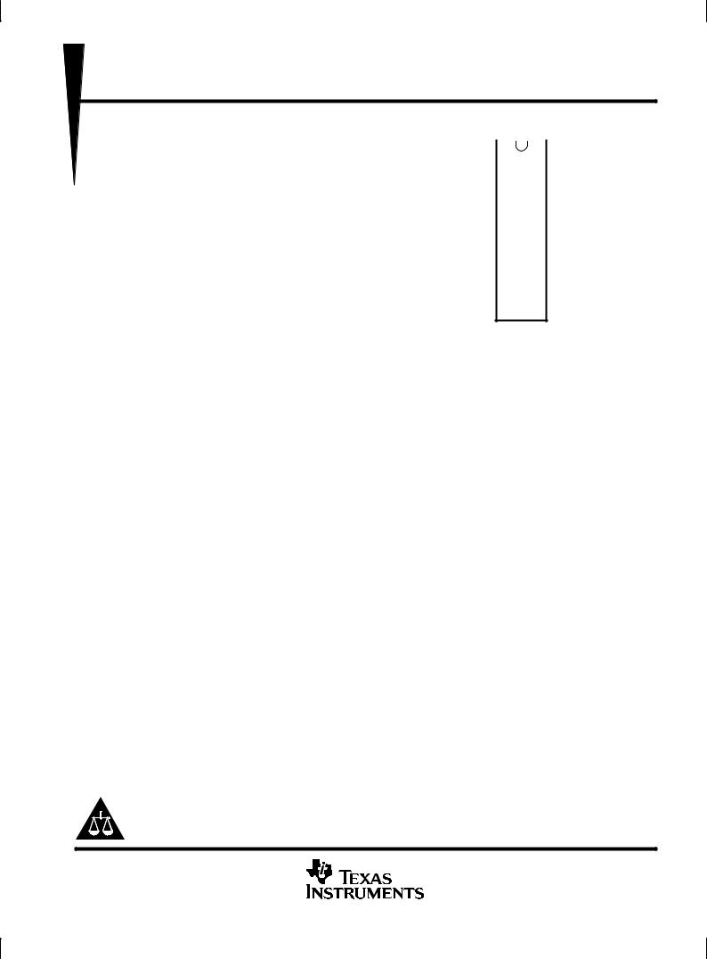
PW OR NS PACKAGE |
|||||||||
D |
8-Bit Resolution |
|
|
|
|
|
|
|
(TOP VIEW) |
|
||||
|
|
|
|
|
|
|
|
|
|
DGND |
||||
|
|
|
|
|
|
|
|
|
|
|
|
|
|
|
D |
Differential Linearity Error |
|
|
OE |
|
|
1 |
24 |
|
|||||
|
|
|
|
|
||||||||||
|
|
± |
|
± |
|
° |
DGND |
|
2 |
23 |
|
REFB |
||
|
± |
|
0.3 LSB Typ, |
|
1 LSB Max (25 C) |
|
|
|
|
|
|
|
|
|
|
± ± 1 LSB Max |
|
|
|
D1(LSB) |
|
3 |
22 |
|
REFBS |
||||
D |
Integral Linearity Error |
|
|
D2 |
|
4 |
21 |
|
AGND |
|||||
|
± ± 0.6 LSB, ± 0.75 LSB Max (25°C) |
|
D3 |
|
5 |
20 |
|
AGND |
||||||
|
± ± 1 LSB Max |
|
|
|
|
D4 |
|
6 |
19 |
|
ANALOG IN |
|||
D Maximum Conversion Rate of |
|
|
D5 |
|
7 |
18 |
|
VDDA |
||||||
|
|
D6 |
|
8 |
17 |
|
REFT |
|||||||
|
40 Megasamples Per Second (MSPS) Max |
|
|
|
||||||||||
|
|
D7 |
|
|
|
|
REFTS |
|||||||
|
|
|
9 |
16 |
|
|||||||||
D Internal Sample and Hold Function |
|
|
|
|||||||||||
D8(MSB) |
|
10 |
15 |
|
VDDA |
|||||||||
|
|
|||||||||||||
D 5-V Single Supply Operation |
|
|
|
|||||||||||
|
VDDD |
|
11 |
14 |
|
VDDA |
||||||||
D Low Power Consumption . . . 85 mW Typ |
CLK |
|
12 |
13 |
|
VDDD |
||||||||
|
|
|||||||||||||
DAnalog Input Bandwidth . . . ≥ 75 MHz Typ
DInternal Reference Voltage Generators
applications |
AVAILABLE OPTIONS |
||||
|
|
|
|||
TA |
PACKAGE |
||||
|
|
||||
D |
Quadrature Amplitude Modulation (QAM) |
TSSOP (PW) |
SOP (NS) |
||
|
and Quadrature Phase Shift Keying (QPSK) |
|
|
|
|
|
± 0°C to 70°C |
TLC5540CPW |
TLC5540CNSLE |
||
|
Demodulators |
||||
|
± 40°C to 85°C |
TLC5540IPW |
TLC5540INSLE |
||
D |
Digital Television |
|
|
|
|
|
|
|
|||
D Charge-Coupled Device (CCD) Scanners |
|
|
|
||
D |
Video Conferencing |
|
|
|
|
D Digital Set-Top Box |
|
|
|
||
D |
Digital Down Converters |
|
|
|
|
D High-Speed Digital Signal Processor |
|
|
|
||
|
Front End |
|
|
|
|
description
The TLC5540 is a high-speed, 8-bit analog-to-digital converter (ADC) that converts at sampling rates up to 40 megasamples per second (MSPS). Using a semiflash architecture and CMOS process, the TLC5540 is able to convert at high speeds while still maintaining low power consumption and cost. The analog input bandwidth of 75 MHz (typ) makes this device an excellent choice for undersampling applications. Internal resistors are provided to generate 2-V full-scale reference voltages from a 5-V supply, thereby reducing external components. The digital outputs can be placed in a high impedance mode. The TLC5540 requires only a single 5-V supply for operation.
Please be aware that an important notice concerning availability, standard warranty, and use in critical applications of Texas Instruments semiconductor products and disclaimers thereto appears at the end of this data sheet.
PRODUCTION DATA information is current as of publication date. Products conform to specifications per the terms of Texas Instruments standard warranty. Production processing does not necessarily include testing of all parameters.
Copyright 1999, Texas Instruments Incorporated
POST OFFICE BOX 655303 •DALLAS, TEXAS 75265 |
1 |
TLC5540
8-BIT HIGH-SPEED ANALOG-TO-DIGITAL CONVERTER
SLAS105C ± JANUARY 1995 ± REVISED MAY 1999
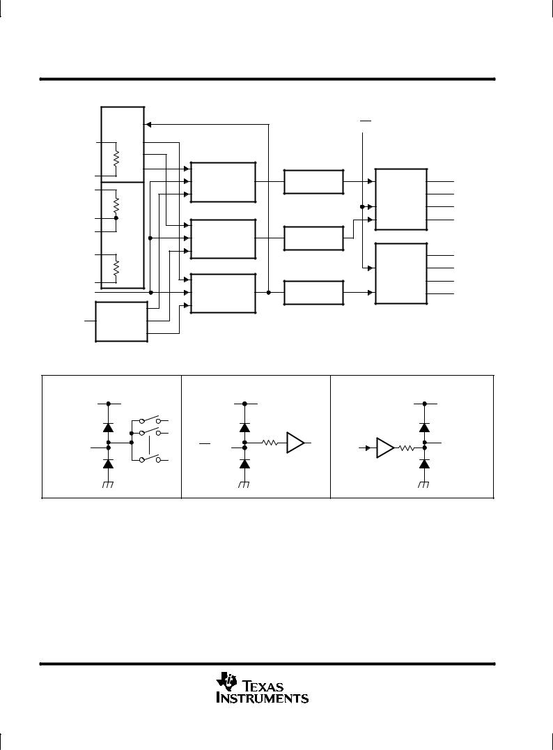
functional block diagram
|
Resistor |
|
|
Reference |
|
|
Divider |
|
REFB |
|
|
|
270 Ω |
|
|
NOM |
|
REFT |
Lower Sampling |
|
Comparators |
||
REFBS |
||
(4 Bit) |
||
|
80 Ω |
|
AGND |
NOM |
|
|
||
AGND |
Lower Sampling |
|
|
Comparators |
|
VDDA |
(4 Bit) |
|
|
||
|
320 Ω |
|
REFTS |
NOM |
|
Upper Sampling |
||
ANALOG IN |
Comparators |
|
|
(4 Bit) |
|
CLK |
Clock |
|
Generator |
||
|
OE |
|
|
Lower Encoder |
D1(LSB) |
|
(4 Bit) |
||
D2 |
||
Lower Data |
||
Latch |
D3 |
|
|
||
|
D4 |
|
Lower Encoder |
|
|
(4 Bit) |
|
|
|
D5 |
|
Upper Data |
D6 |
|
Latch |
D7 |
|
Upper Encoder |
||
D8(MSB) |
||
(4 Bit) |
||
|
schematics of inputs and outputs |
|
|
EQUIVALENT OF ANALOG INPUT |
EQUIVALENT OF EACH DIGITAL INPUT |
EQUIVALENT OF EACH DIGITAL OUTPUT |
VDDA |
VDDD |
VDDD |
ANALOG IN |
OE, CLK |
D1 ± D8 |
|
||
AGND |
DGND |
DGND |
2 |
POST OFFICE BOX 655303 •DALLAS, TEXAS 75265 |
|
|
|
|
|
|
|
|
|
TLC5540 |
|
|
|
|
|
|
8-BIT HIGH-SPEED ANALOG-TO-DIGITAL CONVERTER |
|||||
|
|
|
|
|
|
|
|
|
SLAS105C ± JANUARY 1995 ± REVISED MAY 1999 |
|
|
|
|
|
|
|
|
|
|
|
|
|
|
|
|
|
Terminal Functions |
|||||
|
|
|
|
|
|
|
|
|
|
|
|
|
TERMINAL |
I/O |
|
|
DESCRIPTION |
|
|||
|
NAME |
NO. |
|
|
|
|||||
|
|
|
|
|
|
|
|
|||
|
|
|
|
|
|
|
|
|
|
|
|
AGND |
20, 21 |
|
Analog ground |
|
|||||
|
|
|
|
|
|
|
|
|
|
|
|
ANALOG IN |
19 |
I |
Analog input |
|
|||||
|
|
|
|
|
|
|
|
|
|
|
|
CLK |
12 |
I |
Clock input |
|
|||||
|
|
|
|
|
|
|
|
|
|
|
|
DGND |
2, 24 |
|
Digital ground |
|
|||||
|
|
|
|
|
|
|
|
|
|
|
|
D1 ± D8 |
3 ± 10 |
O |
Digital data out. D1:LSB, D8:MSB |
|
|||||
|
|
|
|
|
|
|
|
|
|
|
|
|
|
1 |
I |
Output enable. When |
|
= L, data is enabled. When |
|
= H, D1±D8 is high impedance. |
|
|
OE |
|
OE |
OE |
|
|||||
|
|
|
|
|
|
|||||
|
VDDA |
14, 15, 18 |
|
Analog VDD |
|
|||||
|
VDDD |
11, 13 |
|
Digital VDD |
|
|||||
|
REFB |
23 |
I |
ADC reference voltage in (bottom) |
|
|||||
|
|
|
|
|
|
|||||
|
REFBS |
22 |
|
Reference voltage (bottom). When using the internal voltage divider to generate a nominal 2-V reference, |
|
|||||
|
|
|
|
|
the REFBS terminal is shorted to the REFB terminal and the REFTS terminal is shorted to the REFT terminal |
|
||||
|
|
|
|
|
(see Figure 13 and Figure 14). |
|
||||
|
|
|
|
|
|
|||||
|
REFT |
17 |
I |
Reference voltage in (top) |
|
|||||
|
|
|
|
|
|
|||||
|
REFTS |
16 |
|
Reference voltage (top). When using the internal voltage divider to generate a nominal 2-V reference, the |
|
|||||
|
|
|
|
|
REFTS terminal is shorted to the REFT terminal and the REFBS terminal is shorted to the REFB terminal |
|
||||
|
|
|
|
|
(see Figure 13 and Figure 14). |
|
||||
|
|
|
|
|
|
|
|
|
|
|
absolute maximum ratings over operating free-air temperature range (unless otherwise noted)²
Supply voltage, VDDA, VDDD . . . . . . . . . . . . . . . . . . . . . . . . . . . . . . . . . . . . . . . . . . . . . . . . . . . . . . |
. . . . . . . . . . . 7 V |
Reference voltage input range, VI(REFT), VI(REFB), VI(REFBS), VI(REFTS) . . . . . . . . . . . . . . . |
AGND to VDDA |
Analog input voltage range, VI(ANLG) . . . . . . . . . . . . . . . . . . . . . . . . . . . . . . . . . . . . . . . . . . . . . . . |
AGND to VDDA |
Digital input voltage range, VI(DGTL) . . . . . . . . . . . . . . . . . . . . . . . . . . . . . . . . . . . . . . . . . . . . . . . . |
DGND to VDDD |
Digital output voltage range, VO(DGTL) . . . . . . . . . . . . . . . . . . . . . . . . . . . . . . . . . . . . . . . . . . . . . |
DGND to VDDD |
Operating free-air temperature range, TA: TLC5540C . . . . . . . . . . . . . . . . . . . . . . . . . . . . . . . . . |
. . 0°C to 70°C |
TLC5540I . . . . . . . . . . . . . . . . . . . . . . . . . . . . . . . . . |
±40°C to 85°C |
Storage temperature range, Tstg . . . . . . . . . . . . . . . . . . . . . . . . . . . . . . . . . . . . . . . . . . . . . . . . . . . |
±55°C to 150°C |
²Stresses beyond those listed under ªabsolute maximum ratingsº may cause permanent damage to the device. These are stress ratings only, and functional operation of the device at these or any other conditions beyond those indicated under ªrecommended operating conditionsº is not implied. Exposure to absolute-maximum-rated conditions for extended periods may affect device reliability.
POST OFFICE BOX 655303 •DALLAS, TEXAS 75265 |
3 |

TLC5540
8-BIT HIGH-SPEED ANALOG-TO-DIGITAL CONVERTER
SLAS105C ± JANUARY 1995 ± REVISED MAY 1999
recommended operating conditions
|
|
|
MIN |
NOM |
MAX |
UNIT |
|
|
|
|
|
|
|
|
|
VDDA ± AGND |
4.75 |
5 |
5.25 |
V |
Supply voltage |
|
VDDD ± AGND |
4.75 |
5 |
5.25 |
|
|
|
|||||
|
|
AGND ± DGND |
± 100 |
0 |
100 |
mV |
|
|
|
|
|
|
|
Reference input voltage (top), VI(REFT) |
|
VI(REFB)+1.8 |
VI(REFB)+2 |
VDDA |
V |
|
Reference input voltage (bottom), VI(REFB) |
|
0 |
0.6 |
VI(REFT)±1.8 |
V |
|
Analog input voltage range, VI(ANLG) (see Note 1) |
VI(REFB) |
|
VI(REFT) |
V |
||
Full scale voltage, VI(REFT) ± VI(REFB) |
|
1.8 |
|
5 |
V |
|
High-level input voltage, VIH |
|
4 |
|
|
V |
|
Low-level input voltage, VIL |
|
|
|
1 |
V |
|
Pulse duration, clock high, tw(H) |
|
12.5 |
|
|
ns |
|
Pulse duration, clock low, tw(L) |
|
12.5 |
|
|
ns |
|
Operating free-air temperature, TA |
|
TLC5540C |
0 |
|
70 |
°C |
|
|
|
|
|
|
|
|
TLC5540I |
± 40 |
|
85 |
°C |
|
|
|
|
||||
|
|
|
|
|
|
|
NOTE 1: 1.8 V ≤ VI(REFT) ± VI(REFB) < VDD
4 |
POST OFFICE BOX 655303 •DALLAS, TEXAS 75265 |
TLC5540 8-BIT HIGH-SPEED ANALOG-TO-DIGITAL CONVERTER
SLAS105C ± JANUARY 1995 ± REVISED MAY 1999
electrical characteristics at VDD = 5 V, VI(REFT) = 2.6 V, VI(REFB) = 0.6 V, fs = 40 MSPS, TA = 25°C
(unless otherwise noted)
|
PARAMETER |
|
|
TEST CONDITIONS² |
|
MIN |
TYP |
MAX |
UNIT |
|||
EL |
Linearity error, integral |
|
|
|
TA = 25°C |
|
|
± 0.6 |
|
± 1 |
|
|
|
f = 40 MSPS, |
TA = MIN to MAX |
|
|
|
|
± 1 |
|
||||
|
|
|
|
|
|
|
|
|||||
|
|
|
s |
|
|
|
|
|
|
|
LSB |
|
|
|
|
V = 0.6 V to 2.6 V |
° |
|
|
± |
0.3 |
± |
0.75 |
||
ED |
Linearity error, differential |
|
I |
TA = 25 C |
|
|
|
|
|
|||
|
|
|
TA = MIN to MAX |
|
|
|
|
± 1 |
|
|||
|
|
|
|
|
|
|
|
|
|
|||
|
Self bias (1), VRB |
|
Short REFB to REFBS |
See Figure 13 |
|
0.57 |
0.61 |
|
0.65 |
|
||
|
Self bias (1), VRT |
|
Short REFT to REFTS |
|
2.47 |
2.63 |
|
2.80 |
V |
|||
|
|
|
|
|
||||||||
|
Self bias (2), VRB |
|
Short REFB to AGND |
See Figure 14 |
|
|
AGND |
|
|
|||
|
|
|
|
|
|
|
||||||
|
Self bias (2), VRT |
|
Short REFT to REFTS |
|
2.18 |
2.29 |
|
2.4 |
|
|||
|
|
|
|
|
|
|||||||
Iref |
Reference-voltage current |
|
VI(REFT) ± VI(REFB) = 2 V |
|
5.2 |
|
7.5 |
|
12 |
mA |
||
Rref |
Reference-voltage resistor |
|
Between REFT and REFB terminals |
|
165 |
270 |
|
350 |
Ω |
|||
Ci |
Analog input capacitance |
|
VI(ANLG) = 1.5 V + 0.07 Vrms |
|
|
|
4 |
|
|
pF |
||
EZS |
Zero-scale error |
|
VI(REFT) ± VI(REFB) = 2 V |
|
± 18 |
± 43 |
|
± 68 |
mV |
|||
EFS |
Full-scale error |
|
|
± 25 |
|
0 |
|
25 |
||||
|
|
|
|
|
|
|
|
|||||
IIH |
High-level input current |
|
VDD = 5.25 V, |
VIH = VDD |
|
|
|
|
|
5 |
μA |
|
IIL |
Low-level input current |
|
VDD = 5.25 V, |
VIL = 0 |
|
|
|
|
|
5 |
||
|
|
|
|
|
|
|
||||||
IOH |
High-level output current |
|
|
= GND, |
VDD = 4.75 V, |
VOH = VDD ± 0.5 V |
± 1.5 |
|
|
|
|
|
|
OE |
|
|
|
|
mA |
||||||
|
|
|
|
|
|
|
|
|
|
|
|
|
IOL |
Low-level output current |
|
OE = GND, |
VDD = 4.75 V, |
VOL = 0.4 V |
2.5 |
|
|
|
|
||
|
|
|
|
|
|
|||||||
|
High-level |
|
|
|
|
|
|
|
|
|
|
|
IOZH(lkg) |
high-impedance-state |
|
OE |
= VDD, |
VDD = 5.25, |
VOH = VDD |
|
|
|
|
16 |
|
|
output leakage current |
|
|
|
|
|
|
|
|
|
|
μA |
|
|
|
|
|
|
|
|
|
|
|
|
|
|
Low-level |
|
|
|
|
|
|
|
|
|
|
|
|
|
|
|
|
|
|
|
|
|
|
|
|
IOZL(lkg) |
high-impedance-state |
|
OE |
= VDD, |
VDD = 4.75, |
VOL = 0 |
|
|
|
|
16 |
|
|
output leakage current |
|
|
|
|
|
|
|
|
|
|
|
|
|
|
|
|
|
|
|
|
|
|
||
|
|
|
f = 40 MSPS, |
NTSC³ ramp wave input, |
|
|
|
|
|
|
||
IDD |
Supply current |
|
s |
|
|
|
|
17 |
|
27 |
mA |
|
CL 25 pF, |
See Note 2 |
|
|
|
|
|||||||
|
|
|
|
|
|
|
|
|
||||
² Conditions marked MIN or MAX are as stated in recommended operating conditions. ³ National Television System Committee
NOTE 2: Supply current specification does not include Iref.
POST OFFICE BOX 655303 •DALLAS, TEXAS 75265 |
5 |
TLC5540
8-BIT HIGH-SPEED ANALOG-TO-DIGITAL CONVERTER
SLAS105C ± JANUARY 1995 ± REVISED MAY 1999
operating characteristics at VDD = 5 V, VRT = 2.6 V, VRB = 0.6 V, fs = 40 MSPS, TA = 25°C (unless otherwise noted)
|
PARAMETER |
TEST CONDITIONS² |
MIN |
TYP |
MAX |
UNIT |
||
fs |
Maximum conversion rate |
TA = MIN to MAX |
40 |
|
|
MSPS |
||
fs |
Minimum conversion rate |
TA = MIN to MAX |
|
5 |
|
MSPS |
||
BW |
Analog input full-power bandwidth |
At ± 3 dB, |
|
VI(ANLG) = 2 Vpp |
|
75 |
|
MHz |
tpd |
Delay time, digital output |
CL ≤ 10 pF (see Note 3) |
|
9 |
15 |
ns |
||
tPHZ |
Disable time, output high to Hi-Z |
CL ≤ 15 pF, |
|
IOH = ± 4.5 mA |
|
|
20 |
ns |
tPLZ |
Disable time, output low to Hi-Z |
CL ≤ 15 pF, |
|
IOL = 5 mA |
|
|
20 |
ns |
tPZH |
Enable time, Hi-Z to output high |
CL ≤ 15 pF, |
|
IOH = ± 4.5 mA |
|
|
15 |
ns |
tPZL |
Enable time, Hi-Z to output low |
CL ≤ 15 pF, |
|
IOL = 5 mA |
|
|
15 |
ns |
|
Differential gain |
NTSC 40 IRE³ |
modulation wave, |
|
1% |
|
|
|
|
Differential phase |
fs = 14.3 MSPS |
|
0.7 |
|
degrees |
||
tAJ |
Aperture jitter time |
|
|
|
|
30 |
|
ps |
td(s) |
Sampling delay time |
|
|
|
|
4 |
|
ns |
|
|
|
|
fI = 1 MHz |
|
47 |
|
|
|
|
fs = 20 MSPS |
|
fI = 3 MHz |
44 |
47 |
|
|
|
|
|
fI = 6 MHz |
|
46 |
|
|
|
|
|
|
|
|
|
|
||
SNR |
Signal-to-noise ratio |
|
|
fI = 10 MHz |
|
45 |
|
dB |
|
|
|
|
fI = 3 MHz |
|
45.2 |
|
|
|
|
fs = 40 MSPS |
|
fI = 6 MHz |
42 |
44 |
|
|
|
|
|
|
fI = 10 MHz |
|
42 |
|
|
|
|
|
|
fI = 1 MHz |
|
7.64 |
|
|
|
|
fs = 20 MSPS |
|
fI = 3 MHz |
|
7.61 |
|
|
ENOB |
Effective number of bits |
|
fI = 6 MHz |
|
7.47 |
|
Bits |
|
|
|
|
|
|||||
|
|
fI = 10 MHz |
|
7.16 |
|
|||
|
|
|
|
|
|
|
||
|
|
fs = 40 MSPS |
|
fI = 3 MHz |
|
7 |
|
|
|
|
|
fI = 6 MHz |
|
6.8 |
|
|
|
|
|
|
|
|
|
|
||
|
|
|
|
fI = 1 MHz |
|
43 |
|
|
|
|
fs = 20 MSPS |
|
fI = 3 MHz |
35 |
42 |
|
|
THD |
Total harmonic distortion |
|
fI = 6 MHz |
|
41 |
|
dBc |
|
|
|
|
|
|||||
|
|
fI = 10 MHz |
|
38 |
|
|||
|
|
|
|
|
|
|
||
|
|
fs = 40 MSPS |
|
fI = 3 MHz |
|
40 |
|
|
|
|
|
fI = 6 MHz |
|
38 |
|
|
|
|
|
|
|
|
|
|
||
|
Spurious free dynamic range |
fs = 20 MSPS |
|
fI = 3 MHz |
41 |
46 |
|
dBc |
|
fs = 40 MSPS |
|
|
42 |
|
|||
|
|
|
|
|
|
|
||
² Conditions marked MIN or MAX are as stated in recommended operating conditions. ³ Institute of Radio Engineers
NOTE 3: CL includes probe and jig capacitance.
6 |
POST OFFICE BOX 655303 •DALLAS, TEXAS 75265 |
 Loading...