


Texas Instruments TL3016CPWLE, TL3016CPW, TL3016CDR, TL3016CD, TL3016IPWR Datasheet
...TL3016, TL3016Y
ULTRA-FAST LOW-POWER
PRECISION COMPARATORS
|
SLCS130D ± MARCH 1997 ± REVISED MARCH 2000 |
|
|
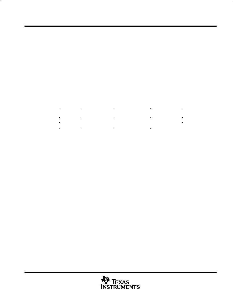
D Ultrafast Operation . . . 7.6 ns (Typ) |
D AND PW PACKAGE |
|
(TOP VIEW) |
DLow Positive Supply Current
|
10.6 mA (Typ) |
|
|
|
|
|
|
|
|
|
|
|
VCC+ |
|
|
1 |
8 |
|
|
Q OUT |
|||
D |
Operates From a Single 5-V Supply or From |
IN + |
|
|
2 |
7 |
|
|
Q OUT |
||
|
a Split ± 5-V Supply |
IN ± |
|
|
3 |
6 |
|
|
GND |
||
D |
Complementary Outputs |
VCC± |
|
|
4 |
5 |
|
|
LATCH ENABLE |
||
DLow Offset Voltage
DNo Minimum Slew Rate Requirement
DOutput Latch Capability
D Functional Replacement to the LT1016 |
|
symbol (each comparator) |
|
|
|
|||||||||||
|
|
|
|
|
|
|
|
|
|
|||||||
description |
|
|
|
|
|
|
|
|
|
IN + |
|
|
|
Q OUT |
|
|
|
|
|
|
|
|
|
|
|
|
|
|
|
|
|
|
|
The TL3016 is an ultrafast comparator designed |
|
|
IN ± |
|
|
|
Q OUT |
|
|
|||||||
to interface directly to TTL logic while operating |
|
|
|
|
|
|
|
|
|
|||||||
from either a single 5-V power supply or dual |
|
|
|
|
|
|
|
|
|
|||||||
± 5-V supplies. It features extremely tight offset |
|
|
|
|
|
|
|
|
|
|||||||
voltage and high gain for precision applications. It |
|
|
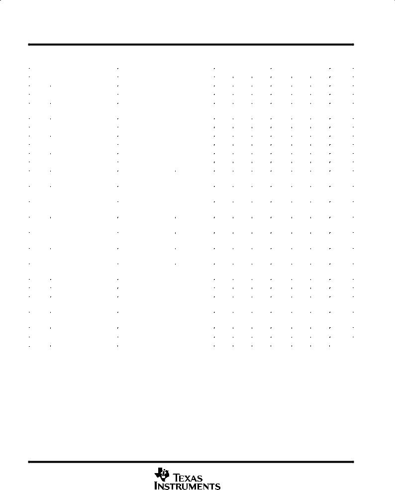
POSITIVE SUPPLY CURRENT |
|
||||||||||||
has complementary outputs that can be latched |
|
|
|
|||||||||||||
|
|
|
|
vs |
|
|
|
|
||||||||
using the LATCH ENABLE terminal. Figure 1 |
|
|
|
|
|
|
|
|
||||||||
|
|
FREE-AIR TEMPERATURE |
|
|
||||||||||||
shows |
the |
positive |
supply |
current |
of |
this |
|
15 |
|
|
|
|
|
|
|
|
comparator. The TL3016 only requires 10.6 mA |
|
|
|
|
|
|
|
|
||||||||
|
14 |
VCC = ± 5 V |
|
|
|
|
|
|||||||||
(typical) to achieve a propagation delay of 7.6 ns. |
|
|
|
|
|
|
||||||||||
mA |
|
|
|
|
|
|
|
|||||||||
The TL3016 is a pin-for-pin functional replace- |
13 |
|
|
|
|
|
|
|
||||||||
± |
|
|
|
|
|
|
|
|||||||||
ment for the LT1016 comparator, offering higher |
|
|
|
|
|
|
|
|
||||||||
Current |
12 |
|
|
|
|
|
|
|
||||||||
speed operation but consuming half the power. |
|
|
|
|
|
|
|
|||||||||
|
|
|
|
|
|
|
|
|||||||||
|
|
|
|
|
|
|
|
|
||||||||
|
|
|
|
|
|
|
|
Supply |
11 |
|
|
|
|
|
|
|
|
|
AVAILABLE OPTIONS |
|
|
|
|
|
|
|
|
|
|
|
|
||
|
|
|
|
|
|
|
|
|
|
|
|
|
|
|
||
|
|
PACKAGED DEVICES |
|
|
|
|
|
10 |
|
|
|
|
|
|
|
|
|
|
|
|
CHIP |
|
|
|
|
|
|
|
|
|
|
||
|
|
(D) |
|
|
|
|
Positive |
8 |
|
|
|
|
|
|
|
|
TA |
|
SMALL |
TSSOP |
|
|
FORM³ |
|
9 |
|
|
|
|
|
|
|
|
|
OUTLINE² |
(PW) |
|
|
(Y) |
|
|
|
|
|
|
|
|
|
|
|
|
|
|
|
|
|
|
|
|
|
|
|
|
|
|
||
0°C to 70°C |
TL3016CD |
TL3016CPWLE |
TL3016Y |
± |
|
|
|
|
|
|
|
|
||||
CC |
7 |
|
|
|
|
|
|
|
||||||||
± 40°C to 85°C |
TL3016ID |
TL3016IPWLE |
|
Ð |
|
|
|
|
|
|
|
|
||||
|
|
|
|
|
|
|
|
|
|
|||||||
|
|
I |
|
|
|
|
|
|
|
|
||||||
² The PW packages are available left-ended taped and reeled only. |
|
6 |
|
|
|
|
|
|
|
|||||||
³ Chip forms are tested at T = 25°C only. |
|
|
|
|
|
5 |
|
|
|
|
|
|
|
|||
|
|
A |
|
|
|
|
|
|
|
|
|
|
|
|
|
|
|
|
|
|
|
|
|
|
|
± 50 |
± 25 |
0 |
25 |
50 |
75 |
100 |
125 |
|
|
|
|
|
|
|
|
|
|
TA ± Free-Air Temperature ± °C |
|
|
||||
|
|
|
|
|
|
|
|
|
|
|
|
Figure 1 |
|
|
|
|
Please be aware that an important notice concerning availability, standard warranty, and use in critical applications of Texas Instruments semiconductor products and disclaimers thereto appears at the end of this data sheet.
PRODUCTION DATA information is current as of publication date. Products conform to specifications per the terms of Texas Instruments standard warranty. Production processing does not necessarily include testing of all parameters.
Copyright 2000, Texas Instruments Incorporated
POST OFFICE BOX 655303 •DALLAS, TEXAS 75265 |
1 |

TL3016, TL3016Y
ULTRA-FAST LOW-POWER
PRECISION COMPARATORS
SLCS130D ± MARCH 1997 ± REVISED MARCH 2000
TL3016Y chip information
This chip displays characteristics similar to the TL3016C. Thermal compression or ultrasonic bonding may be used on the doped-aluminum bonding pads. Chips may be mounted with conductive epoxy or a gold-silicon preform.
BONDING PAD ASSIGNMENTS
|
|
|
|
(1) |
(1) |
|
|
(8) |
|
|
|
|
|
|
|||||
|
|
(1) |
|
|
|
|
|
||
|
|
|
|
|
|
|
|
(7) |
|
|
|
(2) |
|
|
|
|
|
||
|
|
|
|
|
|
|
|
||
55 |
|
|
|
|
|
|
|||
|
|
|
|
|
|
|
|
(6) |
|
|
|
(3) |
|
|
|
|
|
||
|
|
|
|
|
|
|
|
(6) |
|
|
|
(4) |
|
(5) |
(6) |
|
|||
|
|
|
|
|
|
|
|
|
|
|
|
|
|
|
|
|
|
|
|
|
|
|
|
|
|
63 |
|
|
|
VCC+
(5)(1)
LATCH ENABLE
(2)(8)
IN+ |
+ |
|
Q OUT |
IN± |
(3) |
|
Q OUT |
± |
(7) |
||
|
|
|
(4)
(6)
VCC ± GND
CHIP THICKNESS: 10 MILS TYPICAL
BONDING PADS: 4 × 4 MILS MINIMUM
TJ max = 150°C
TOLERANCES ARE ± 10%.
ALL DIMENSIONS ARE IN MILS.
TERMINALS 1 AND 6 CAN BE CONNECTED TO MULTIPLE PADS.
COMPONENT COUNT
Bipolars |
53 |
MOSFETs |
49 |
Resistors |
46 |
Capacitors |
14 |
2 |
POST OFFICE BOX 655303 •DALLAS, TEXAS 75265 |
TL3016, TL3016Y
ULTRA-FAST LOW-POWER
PRECISION COMPARATORS
SLCS130D ± MARCH 1997 ± REVISED MARCH 2000
absolute maximum ratings over operating free-air temperature range (unless otherwise noted)²
Supply voltage, VDD (see Note 1) . . . . . . . . . . . . . . . . . . . . . . . . . . . . . . . . . . . . . . . |
. . . . . . . . . . . . . . . ± 7 V to 7 |
V |
Differential input voltage, VID (see Note 2) . . . . . . . . . . . . . . . . . . . . . . . . . . . . . . . |
. . . . . . . . . . . . . . . . . . . . . . 7 |
V |
Input voltage range, VI . . . . . . . . . . . . . . . . . . . . . . . . . . . . . . . . . . . . . . . . . . . . . . . . . |
. . . . . . . . . . . . . . . . . . . . . . 7 |
V |
Input voltage, VI (LATCH ENABLE) . . . . . . . . . . . . . . . . . . . . . . . . . . . . . . . . . . . . . . |
. . . . . . . . . . . . . . . . . . . . . . 7 |
V |
Output current, IO . . . . . . . . . . . . . . . . . . . . . . . . . . . . . . . . . . . . . . . . . . . . . . . . . . . . . |
. . . . . . . . . . . . . . . . . . ± 20 mA |
|
Continuous total power dissipation . . . . . . . . . . . . . . . . . . . . . . . . . . . . . . . . . . . . . |
See Dissipation Rating Table |
|
Operating free-air temperature range, TA . . . . . . . . . . . . . . . . . . . . . . . . . . . . . . . . |
. . . . . . . . . . . . ±40°C to 85°C |
|
Storage temperature range, Tstg . . . . . . . . . . . . . . . . . . . . . . . . . . . . . . . . . . . . . . . . |
. . . . . . . . . . ± 65°C to 150°C |
|
Lead temperature 1,6 mm (1/16 inch) from case for 10 seconds . . . . . . . . . . . . |
. . . . . . . . . . . . . . . . . . . 260°C |
|
² Stresses beyond those listed under ªabsolute maximum ratingsº may cause permanent damage to the device. These are stress ratings only, and functional operation of the device at these or any other conditions beyond those indicated under ªrecommended operating conditionsº is not implied. Exposure to absolute-maximum-rated conditions for extended periods may affect device reliability.
NOTES: 1. All voltage values, except differential voltages, are with respect to network ground. 2. Differential voltages are at IN+ with respect to IN ±.
DISSIPATION RATING TABLE
PACKAGE |
TA ≤ 25°C |
DERATING FACTOR |
TA = 70°C |
|
POWER RATING |
ABOVE TA = 25°C |
POWER RATING |
||
|
||||
D |
725 mW |
5.8 mW/°C |
464 mW |
|
PW |
525 mW |
4.2 mW/°C |
336 mW |
|
|
|
|
|
POST OFFICE BOX 655303 •DALLAS, TEXAS 75265 |
3 |
TL3016, TL3016Y
ULTRA-FAST LOW-POWER
PRECISION COMPARATORS
SLCS130D ± MARCH 1997 ± REVISED MARCH 2000
electrical characteristics at specified operating free-air temperature, VDD = ±5 V, VLE = 0 (unless otherwise noted)
|
PARAMETER |
|
|
TEST CONDITIONS² |
|
|
TL3016C |
|
|
TL3016I |
|
UNIT |
|
|
|
|
|
|
|
|
|
|
|
||||
|
|
|
|
MIN |
TYP³ |
MAX |
MIN |
TYP³ |
MAX |
||||
|
|
|
|
|
|
|
|
||||||
VIO |
Input offset voltage |
|
TA = 25°C |
|
|
|
0.5 |
3 |
|
0.5 |
3 |
mV |
|
|
TA = full range |
|
|
|
|
3.5 |
|
|
3.5 |
||||
|
|
|
|
|
|
|
|
|
|
||||
αVIO |
Temperature coefficient of |
|
|
|
|
|
|
± 4.8 |
|
|
± 4.5 |
|
µV/°C |
input offset voltage |
|
|
|
|
|
|
|
|
|
||||
|
|
|
|
|
|
|
|
|
|
|
|
|
|
|
|
|
|
|
|
|
|
|
|
|
|
|
|
IIO |
Input offset current |
|
TA = 25°C |
|
|
|
0.1 |
0.6 |
|
0.1 |
0.6 |
µA |
|
|
TA = full range |
|
|
|
|
0.9 |
|
|
1.3 |
||||
|
|
|
|
|
|
|
|
|
|
||||
IIB |
Input bias current |
|
TA = 25°C |
|
|
|
6 |
10 |
|
6 |
10 |
µA |
|
|
TA = full range |
|
|
|
|
10 |
|
|
10 |
||||
|
|
|
|
|
|
|
|
|
|
||||
VICR |
Common-mode input |
|
VDD = ± 5 V |
|
|
± 3.75 |
|
3.5 |
± 3.75 |
|
3.5 |
V |
|
voltage range |
|
VDD = 5 V |
|
|
1.25 |
|
3.5 |
1.25 |
|
3.5 |
|||
|
|
|
|
|
|
|
|||||||
CMRR |
Common-mode rejection |
|
±3.75 ≤ VIC ≤ 3.5 V, |
TA = 25°C |
|
80 |
97 |
|
80 |
97 |
|
dB |
|
ratio |
|
|
|
|
|||||||||
|
|
|
|
|
|
|
|
|
|
|
|
|
|
|
|
|
|
|
|
|
|
|
|
|
|
||
|
|
|
Positive supply: 4.6 V ≤ +VDD ≤ 5.4 V, |
|
60 |
72 |
|
60 |
72 |
|
|
||
|
Supply-voltage rejection |
|
TA = 25°C |
|
|
|
|
|
|||||
kSVR |
|
|
|
|
|
|
|
|
|
dB |
|||
ratio |
|
Negative supply: ± 7 V ≤ ±VDD ≤ ± 2 V, |
|
80 |
100 |
|
80 |
100 |
|
||||
|
|
|
|
|
|
||||||||
|
|
|
TA = 25°C |
|
|
|
|
|
|||||
|
|
|
|
|
|
|
|
|
|
|
|
||
|
|
|
I(sink) = 4 mA, |
V+ ≤ 4.6 V, |
|
|
500 |
600 |
|
500 |
600 |
|
|
|
|
|
TA = 25°C |
|
|
|
|
|
|||||
VOL |
Low-level output voltage |
|
|
|
|
|
|
|
|
|
mV |
||
|
I(sink) = 10 mA, |
V+ ≤ 4.6 V, |
|
|
750 |
|
|
750 |
|
||||
|
|
|
TA = 25°C |
|
|
|
|
|
|
|
|||
|
|
|
|
|
|
|
|
|
|
|
|
||
|
|
|
V+ ≤ 4.6 V, |
IO = 1 mA, |
|
3.6 |
3.9 |
|
3.6 |
3.9 |
|
|
|
|
|
|
TA = 25°C |
|
|
|
|
|
|||||
VOH |
High-level output voltage |
|
|
|
|
|
|
|
|
|
V |
||
|
V+ ≤ 4.6 V, |
IO = 10 mA, |
|
3.4 |
3.7 |
|
3.4 |
3.7 |
|
||||
|
|
|
|
|
|
|
|||||||
|
|
|
TA = 25°C |
|
|
|
|
|
|||||
|
|
|
|
|
|
|
|
|
|
|
|
||
IDD |
Positive supply current |
|
TA = full range |
|
|
|
10.6 |
12.5 |
|
10.6 |
12.5 |
mA |
|
|
|
|
|
|
|
|
|
|
|
||||
Negative supply current |
|
|
|
±1.8 |
±1.3 |
|
±2.4 |
±1.3 |
|
||||
|
|
|
|
|
|
|
|
|
|||||
|
|
|
|
|
|
|
|
|
|
|
|
|
|
VIL |
Low-level input voltage |
|
|
|
|
|
|
|
0.8 |
|
|
0.8 |
V |
(LATCH ENABLE) |
|
|
|
|
|
|
|
|
|
||||
|
|
|
|
|
|
|
|
|
|
|
|
|
|
|
|
|
|
|
|
|
|
|
|
|
|
|
|
VIH |
High-level input voltage |
|
|
|
|
|
2 |
|
|
2 |
|
|
V |
(LATCH ENABLE) |
|
|
|
|
|
|
|
|
|
||||
|
|
|
|
|
|
|
|
|
|
|
|
|
|
|
|
|
|
|
|
|
|
|
|
|
|
|
|
|
Low-level input current |
|
VLE = 0 |
|
|
|
0 |
1 |
|
0 |
1 |
|
|
IIL |
(LATCH ENABLE) |
|
|
|
|
|
|
|
|
|
|
|
A |
|
VLE = 2 V |
|
|
|
24 |
39 |
|
24 |
45 |
||||
|
|
|
|
|
|
|
|||||||
|
|
|
|
|
|
|
|
||||||
² Full range for the TL3016C is T = 0°C to 70°C. Full range for the TL3016I is T |
= ± 40°C to 85°C. |
|
|
|
|
|
|||||||
|
A |
|
= 25°C. |
A |
|
|
|
|
|
|
|
||
³ All typical values are measures with T |
|
|
|
|
|
|
|
|
|
|
|||
|
|
A |
|
|
|
|
|
|
|
|
|
|
|
4 |
POST OFFICE BOX 655303 •DALLAS, TEXAS 75265 |
 Loading...