


Texas Instruments TLC339CN10, TLC339CN, TLC339CDR, TLC339CDBR, TLC339CDB Datasheet
...
|
|
|
TLC139, TLC339, TLC339Q |
||||||
|
LinCMOS MICROPOWER QUAD COMPARATORS |
||||||||
|
|
SLCS119 ± DECEMBER 1986 ± REVISED JANUARY 1991 |
|||||||
|
|
|
|
|
|
|
|
|
|
D |
μ |
D, J OR N PACKAGE |
|||||||
|
Very Low Power . . . 200 W Typ at 5 V |
|
|
(TOP VIEW) |
|
|
|||
D Fast Response Time . . . 2.5 μs Typ With |
|
|
|
|
|||||
|
|
|
|
|
|
|
|
||
|
5-mV Overdrive |
1OUT |
|
1 |
14 |
|
|
3OUT |
|
|
|
|
|
||||||
D |
Single Supply Operation: |
|
|
|
|||||
2OUT |
|
2 |
13 |
|
|
4OUT |
|||
|
|
|
|||||||
|
TLC139M . . . 4 V to 16 V |
|
|
|
|||||
|
VDD |
|
3 |
12 |
|
|
GND |
||
|
|
|
|
||||||
|
TLC339M . . . 4 V to 16 V |
|
|
|
|||||
|
|
|
|
||||||
|
2IN ± |
|
4 |
11 |
|
|
4IN + |
||
|
TLC339C . . . 3 V to 16 V |
|
|
|
|||||
|
2IN + |
|
5 |
10 |
|
|
4IN ± |
||
|
|
|
|
||||||
|
TLC339I . . . 3 V to 16 V |
|
|
|
|||||
|
1IN ± |
|
6 |
9 |
|
|
3IN + |
||
|
|
|
|
||||||
|
High Input Impedance . . . 1012 Ω Typ |
|
|
|
|||||
D |
1IN + |
|
7 |
8 |
|
|
3IN ± |
||
|
|
|
|||||||
D Input Offset Voltage Change at Worst Case |
|
|
|
|
|
|
|
|
|
|
|
|
|
|
|
|
|
||
|
Input at Condition Typically 0.23 μV/Month |
|
FK PACKAGE |
|
|
||||
|
Including the First 30 Days |
|
|
|
|||||
|
|
(TOP VIEW) |
|
|
|||||
|
|
|
|
|
|||||
DOn-Chip ESD Protection
description
The TLC139/TLC339 consists of four independent differential-voltage comparators designed to operate from a single supply. It is functionally similar to the LM139/LM339 family but uses 1/20th the power for similar response times. The open-drain MOS output stage interfaces to a variety of leads and supplies, as well as wired logic functions. For a similar device with a push-pull output configuration, see the TLC3704 data sheet.
|
2OUT |
1OUT |
NC |
3OUT |
3OUT |
|
VDD |
3 |
2 |
1 |
20 19 |
GND |
|
4 |
|
|
|
18 |
||
NC |
5 |
|
|
|
17 |
NC |
2IN ± |
6 |
|
|
|
16 |
4IN + |
NC |
7 |
|
|
|
15 |
NC |
2IN + |
8 |
|
|
|
14 |
4IN ± |
|
9 |
10 11 12 13 |
|
|||
|
1IN ± |
1IN + |
NC |
3IN ± |
3IN + |
|
NC ± No internal connection
The Texas Instruments LinCMOS process offers superior analog performance to standard CMOS processes. Along with the standard CMOS advantages of low power without sacrificing speed, high input impedance, and low bias currents, the LinCMOS process offers extremely stable input offset voltages, even with differential input stresses of several volts. This characteristic makes it possible to build reliable CMOS comparators.
symbol (each comparator)
IN +
OUT
IN ±
AVAILABLE OPTIONS
|
VIOmax |
|
PACKAGE |
|
||
TA |
|
|
|
|
||
SMALL OUTLINE |
CHIP CARRIER |
CERAMIC DIP |
PLASTIC DIP |
|||
AT 25°C |
||||||
|
|
(D) |
(FK) |
(J) |
(P) |
|
0°C to 70°C |
5 mV |
TLC339CD |
Ð |
Ð |
TLC339CN |
|
|
|
|
|
|
|
|
± 40°C to 85°C |
5 mV |
TLC339ID |
Ð |
Ð |
TLC339IN |
|
|
|
|
|
|
|
|
± 40°C to 125°C |
5 mV |
TLC339QD |
Ð |
Ð |
TLC339QN |
|
|
|
|
|
|
|
|
± 55°C to 125°C |
5 mV |
TLC339MD |
TLC139MFK |
TLC139MJ |
TLC339MN |
|
|
|
|
|
|
|
|
The D package is available taped and reeled. Add the suffix R to the device type (e.g., TLC339CDR).
LinCMOS is a trademark of Texas Instruments Incorporated.
PRODUCTION DATA information is current as of publication date. Products conform to specifications per the terms of Texas Instruments standard warranty. Production processing does not necessarily include testing of all parameters.
Copyright 1991, Texas Instruments Incorporated
POST OFFICE BOX 655303 •DALLAS, TEXAS 75265 |
1 |
TLC139, TLC339, TLC339Q
LinCMOS MICROPOWER QUAD COMPARATORS
SLCS119 ± DECEMBER 1986 ± REVISED JANUARY 1991
description (continued)
The TLC139M and TLC339M are characterized for operation over the full military temperature range of ±55°C to 125°C. The TLC339C is characterized for operation over the commercial temperature range of 0°C to 70°C. The TLC339I is characterized for operation over the industrial temperature range of ±40°C to 85°C. The TLC339Q is characterized for operation over the extended industrial temperature range of ±40°C to 125°C.
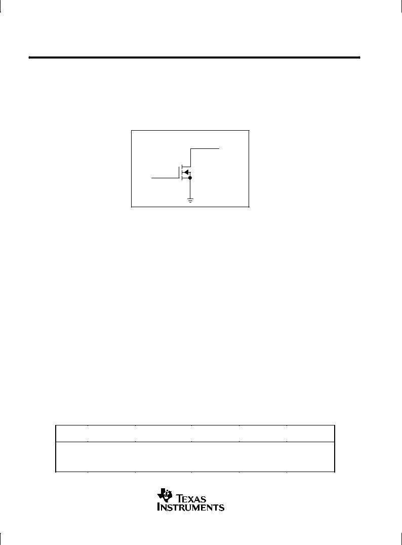
output schematic
OPEN-DRAIN CMOS OUTPUT
Output
absolute maximum ratings over operating free-air temperature range (unless otherwise noted)²
Supply voltage range, VDD (see Note 1) . . . . . . . . . . . . . . . . . . . . . . . . . . . . . . . . . |
. . . . . . . . . . . |
. ±0.3 V to 18 V |
Differential input voltage, VID (see Note 2) . . . . . . . . . . . . . . . . . . . . . . . . . . . . . . . |
. . . . . . . . . . . . |
. . . . . . . . ± 18 V |
Input voltage range, VI . . . . . . . . . . . . . . . . . . . . . . . . . . . . . . . . . . . . . . . . . . . . . . . . . |
. . . . . . . . . . . . |
±0.3 V to VDD |
Output voltage range, VO . . . . . . . . . . . . . . . . . . . . . . . . . . . . . . . . . . . . . . . . . . . . . . |
. . . . . . . . . . . . |
±0.3 V to VDD |
Input current, II . . . . . . . . . . . . . . . . . . . . . . . . . . . . . . . . . . . . . . . . . . . . . . . . . . . . . . . |
. . . . . . . . . . . . |
. . . . . . . ± 5 mA |
Output current, IO (each output) . . . . . . . . . . . . . . . . . . . . . . . . . . . . . . . . . . . . . . . . |
. . . . . . . . . . . . |
. . . . . . . 20 mA |
Total supply current into VDD . . . . . . . . . . . . . . . . . . . . . . . . . . . . . . . . . . . . . . . . . . . |
. . . . . . . . . . . . |
. . . . . . . 40 mA |
Total current out of GND . . . . . . . . . . . . . . . . . . . . . . . . . . . . . . . . . . . . . . . . . . . . . . . |
. . . . . . . . . . . . |
. . . . . . . 60 mA |
Continuous total dissipation . . . . . . . . . . . . . . . . . . . . . . . . . . . . . . . . . . . . . . . . . . . |
See Dissipation Rating Table |
|
Operating free-air temperature range, TA: TLC139M . . . . . . . . . . . . . . . . . . . . . . . |
. . . . . . . . . . . |
±55°C to 125°C |
TLC339C . . . . . . . . . . . . . . . . . . . . . . . |
. . . . . . . . . . . . |
. . 0°C to 70°C |
TLC339I . . . . . . . . . . . . . . . . . . . . . . . . |
. . . . . . . . . . . . |
±40°C to 85°C |
TLC339M . . . . . . . . . . . . . . . . . . . . . . . |
. . . . . . . . . . . |
±55°C to 125°C |
TLC339Q . . . . . . . . . . . . . . . . . . . . . . . |
. . . . . . . . . . . |
±40°C to 125°C |
Storage temperature range . . . . . . . . . . . . . . . . . . . . . . . . . . . . . . . . . . . . . . . . . . . . . |
. . . . . . . . . . . |
±65°C to 150°C |
Case temperature for 60 seconds: FK package . . . . . . . . . . . . . . . . . . . . . . . . . . . |
. . . . . . . . . . . . |
. . . . . . . 260°C |
Lead temperature 1,6 mm (1/16 inch) from case for 10 seconds: D or N package . . . . . . . . . |
. . . . . . . 260°C |
|
Lead temperature 1,6 mm (1/16 inch) from case for 60 seconds: J package . . |
. . . . . . . . . . . . |
. . . . . . . 300°C |
² Stresses beyond those listed under ªabsolute maximum ratingsº may cause permanent damage to the device. These are stress ratings only, and functional operation of the device at these or any other conditions beyond those indicated under ªrecommended operating conditionsº is not implied. Exposure to absolute-maximum-rated conditions for extended periods may affect device reliability.
NOTES: 1. All voltage values, except differential voltages, are with respect to network ground. 2. Differential voltages are at IN+ with respect to IN ±.
DISSIPATION RATING TABLE
PACKAGE |
TA ≤ 25°C |
DERATING FACTOR |
TA = 70°C |
TA = 85°C |
TA = 125°C |
|
POWER RATING |
ABOVE TA = 25°C |
POWER RATING |
POWER RATING |
POWER RATING |
||
|
||||||
D |
950 mW |
7.6 mW/°C |
608 mW |
494 mW |
190 mW |
|
FK |
1375 mW |
11.0 mW/°C |
880 mW |
715 mW |
275 mW |
|
J |
1375 mW |
11.0 mW/°C |
880 mW |
715 mW |
275 mW |
|
N |
1150 mW |
9.2 mW/°C |
736 mW |
598 mW |
230 mW |
|
|
|
|
|
|
|
|
|
|
|
|
|
|
2 |
POST OFFICE BOX 655303 •DALLAS, TEXAS 75265 |

LinCMOS |
TLC139, TLC339, TLC339Q |
|||||
MICROPOWER QUAD COMPARATORS |
||||||
|
SLCS119 ± DECEMBER 1986 ± REVISED JANUARY 1991 |
|||||
|
|
|
|
|
|
|
recommended operating conditions |
|
|
|
|
|
|
|
|
|
|
|
||
|
|
TLC139M, TLC339M |
UNIT |
|
||
|
|
|
|
|
|
|
|
|
MIN |
NOM |
MAX |
|
|
|
|
|
|
|||
|
|
|
|
|
|
|
Supply voltage, VDD |
|
4 |
5 |
16 |
V |
|
Common-mode input voltage, VIC |
|
0 |
|
VDD ± 1.5 |
V |
|
Low-level output current, IOL |
|
|
|
20 |
mA |
|
Operating free-air temperature, TA |
|
± 55 |
|
125 |
°C |
|
electrical characteristics at specified operating free-air temperature, VDD = 5 V (unless otherwise noted)
|
PARAMETER |
TEST CONDITIONS² |
TA |
TLC139M, TLC339M |
UNIT |
|||
|
|
|
|
|||||
|
MIN |
TYP |
MAX |
|||||
|
|
|
|
|
|
|||
|
|
|
|
|
|
|
|
|
|
|
VIC = VICRmin, |
VDD = 5 V to 10 V, |
25°C |
|
1.4 |
5 |
|
V |
Input offset voltage |
|
|
|
|
mV |
||
° |
|
|
|
|||||
IO |
|
See Note 3 |
|
± 55 C to |
|
|
10 |
|
|
|
|
125°C |
|
|
|
||
|
|
|
|
|
|
|
|
|
|
|
|
|
|
|
|
|
|
IIO |
Input offset current |
VIC = 2.5 V |
|
25°C |
|
1 |
|
pA |
|
|
|
|
|
|
|||
|
125°C |
|
|
15 |
nA |
|||
|
|
|
|
|
|
|||
|
|
|
|
|
|
|
|
|
IIB |
Input bias current |
VIC = 2.5 V |
|
25°C |
|
5 |
|
pA |
|
|
|
|
|
|
|||
|
125°C |
|
|
30 |
nA |
|||
|
|
|
|
|
|
|||
|
|
|
|
|
|
|
|
|
|
|
|
|
25°C |
0 to |
|
|
|
|
Common-mode input |
|
|
VDD ± 1 |
|
|
|
|
VICR |
|
|
|
|
|
V |
||
voltage range |
|
|
° |
0 to |
|
|
||
|
|
|
|
± 55 C to |
|
|
|
|
|
|
|
|
125°C |
VDD ± 1.5 |
|
|
|
|
|
|
|
25°C |
|
84 |
|
|
|
|
|
|
|
|
|
|
|
CMRR |
Common-mode rejection ratio |
VIC = VICRmin |
|
125°C |
|
84 |
|
dB |
|
|
|
|
± 55°C |
|
84 |
|
|
|
|
|
|
|
|
|
|
|
|
|
|
|
25°C |
|
85 |
|
|
|
|
|
|
|
|
|
|
|
kSVR |
Supply-voltage rejection ratio |
VDD = 5 V to 10 V |
|
125°C |
|
84 |
|
dB |
|
|
|
|
± 55°C |
|
84 |
|
|
|
|
|
|
|
|
|
|
|
VOL |
Low-level output voltage |
VID = ±1 V, |
IOL = 6 mA |
25°C |
|
300 |
400 |
mV |
|
|
|
|
|||||
125°C |
|
|
800 |
|||||
|
|
|
|
|
|
|
||
|
|
|
|
|
|
|
|
|
IOH |
High-level output current |
VID = ±1 V, |
VO = 5 V |
25°C |
|
0.8 |
40 |
nA |
|
|
|
|
|
||||
125°C |
|
|
1 |
μA |
||||
|
|
|
|
|
|
|||
|
|
|
|
|
|
|
|
|
|
Supply current (four |
|
|
25°C |
|
44 |
80 |
|
IDD |
Outputs low, |
No load |
|
|
|
|
μA |
|
± 55°C to |
|
|
|
|||||
comparators) |
|
|
175 |
|||||
|
|
|
125°C |
|
|
|
||
|
|
|
|
|
|
|
|
|
|
|
|
|
|
|
|
|
|
² All characteristics are measured with zero common-mode voltage unless otherwise noted.
NOTE 3: The offset voltage limits given are the maximum values required to drive the output up to 4.5 V or down to 0.3 V with a 2.5-kΩ load to VDD.
POST OFFICE BOX 655303 •DALLAS, TEXAS 75265 |
3 |

TLC139, TLC339, TLC339Q
LinCMOS MICROPOWER QUAD COMPARATORS
SLCS119 ± DECEMBER 1986 ± REVISED JANUARY 1991
recommended operating conditions
|
|
TLC339C |
UNIT |
|
|
|
|
|
|
|
MIN |
NOM |
MAX |
|
|
|
|||
|
|
|
|
|
Supply voltage, VDD |
3 |
5 |
16 |
V |
Common-mode input voltage, VIC |
± 0.2 |
|
VDD ± 1.5 |
V |
Low-level output current, IOL |
|
8 |
20 |
mA |
Operating free-air temperature,TA |
0 |
|
70 |
°C |
electrical characteristics at specified operating free-air temperature, VDD = 5 V (unless otherwise noted)
|
PARAMETER |
TEST CONDITIONS² |
|
TA |
TLC339C |
|
UNIT |
||
|
|
|
|
|
|||||
|
|
MIN |
TYP |
MAX |
|||||
|
|
|
|
|
|
|
|||
|
|
|
|
|
|
|
|
|
|
VIO |
Input offset voltage |
VIC = VICRmin, |
VDD = 5 V to 10 V, |
|
25°C |
|
1.4 |
5 |
mV |
|
|
|
|
|
|||||
See Note 3 |
|
° |
° |
|
|
6.5 |
|||
|
|
|
|
0 C to 70 C |
|
|
|
||
IIO |
Input offset current |
VIC = 2.5 V |
|
|
25°C |
|
1 |
|
pA |
|
|
|
|
|
|
|
|||
|
|
70°C |
|
|
0.3 |
nA |
|||
|
|
|
|
|
|
|
|||
|
|
|
|
|
|
|
|
|
|
IIB |
Input bias current |
VIC = 2.5 V |
|
|
25°C |
|
5 |
|
pA |
|
|
|
|
|
|
|
|||
|
|
70°C |
|
|
0.6 |
nA |
|||
|
|
|
|
|
|
|
|||
|
|
|
|
|
|
|
|
|
|
|
|
|
|
|
25°C |
0 to |
|
|
|
|
Common-mode input |
|
|
|
VDD ± 1 |
|
|
|
|
VICR |
|
|
|
|
|
|
V |
||
voltage range |
|
|
0°C to 70°C |
0 to |
|
|
|||
|
|
|
|
|
|
||||
|
|
|
|
VDD ± 1.5 |
|
|
|
||
|
|
|
|
|
|
|
|
|
|
|
Common-mode rejection |
|
|
|
25°C |
|
84 |
|
|
|
|
|
|
|
|
|
|
|
|
CMRR |
VIC = VICRmin |
|
|
70°C |
|
84 |
|
dB |
|
ratio |
|
|
|
|
|||||
|
|
|
|
0°C |
|
84 |
|
|
|
|
|
|
|
|
|
|
|
||
|
|
|
|
|
|
|
|
|
|
|
Supply-voltage rejection |
|
|
|
25°C |
|
85 |
|
|
|
|
|
|
|
|
|
|
|
|
kSVR |
VDD = 5 V to 10 V |
|
|
70°C |
|
85 |
|
dB |
|
ratio |
|
|
|
|
|||||
|
|
|
|
0°C |
|
85 |
|
|
|
|
|
|
|
|
|
|
|
||
|
|
|
|
|
|
|
|
|
|
VOL |
Low-level output voltage |
VID = ±1 V, |
IOL = 6 mA |
|
25°C |
|
300 |
400 |
mV |
|
|
|
|
|
|||||
|
70°C |
|
|
650 |
|||||
|
|
|
|
|
|
|
|
||
|
|
|
|
|
|
|
|
|
|
IOH |
High-level output current |
VID = ±1 V, |
VO = 5 V |
|
25°C |
|
0.8 |
40 |
nA |
|
|
|
|
|
|
||||
|
70°C |
|
|
1 |
μA |
||||
|
|
|
|
|
|
|
|||
|
|
|
|
|
|
|
|
|
|
IDD |
Supply current (four |
Outputs low, |
No load |
|
25°C |
|
44 |
80 |
μA |
comparators) |
0°C to 70°C |
|
|
100 |
|||||
|
|
|
|
|
|
||||
|
|
|
|
|
|
|
|
|
|
² All characteristics are measured with zero common-mode voltage unless otherwise noted.
NOTE 4: The offset voltage limits given are the maximum values required to drive the output up to 4.5 V or down to 0.3 V with a 2.5-kΩ load to VDD.
4 |
POST OFFICE BOX 655303 •DALLAS, TEXAS 75265 |
LinCMOS |
TLC139, TLC339, TLC339Q |
|||||
MICROPOWER QUAD COMPARATORS |
||||||
|
SLCS119 ± DECEMBER 1986 ± REVISED JANUARY 1991 |
|||||
|
|
|
|
|
|
|
recommended operating conditions |
|
|
|
|
|
|
|
|
|
|
|
|
|
|
|
|
TLC339I |
UNIT |
|
|
|
|
|
|
|
|
|
|
|
MIN |
NOM |
MAX |
|
|
|
|
|
|
|||
|
|
|
|
|
|
|
Supply voltage, VDD |
|
3 |
5 |
16 |
V |
|
Common-mode input voltage, VIC |
|
± 0.2 |
|
VDD ± 1.5 |
V |
|
Low-level output current, IOL |
|
|
8 |
20 |
mA |
|
Operating free-air temperature,TA |
|
0 |
|
70 |
°C |
|
electrical characteristics at specified operating free-air temperature, VDD = 5 V (unless otherwise noted)
|
PARAMETER |
TEST CONDITIONS² |
|
TA |
TLC339I |
|
UNIT |
||
|
|
|
|
|
|||||
|
|
MIN |
TYP |
MAX |
|||||
|
|
|
|
|
|
|
|||
|
|
|
|
|
|
|
|
|
|
VIO |
Input offset voltage |
VIC = VICRmin, |
VDD = 5 V to 10 V, |
25°C |
|
1.4 |
5 |
mV |
|
|
|
|
|
|
|||||
See Note 3 |
|
° |
° |
|
|
7 |
|||
|
|
|
|
± 40 C to 85 C |
|
|
|
||
IIO |
Input offset current |
VIC = 2.5 V |
|
25°C |
|
1 |
|
pA |
|
|
|
|
|
|
|
|
|||
|
85°C |
|
|
1 |
nA |
||||
|
|
|
|
|
|
||||
|
|
|
|
|
|
|
|
|
|
IIB |
Input bias current |
VIC = 2.5 V |
|
25°C |
|
5 |
|
pA |
|
|
|
|
|
|
|
|
|||
|
85°C |
|
|
2 |
nA |
||||
|
|
|
|
|
|
||||
|
|
|
|
|
|
|
|
|
|
|
|
|
|
25°C |
0 to |
|
|
|
|
|
Common-mode input |
|
|
VDD ± 1 |
|
|
|
||
VICR |
|
|
|
|
|
|
V |
||
voltage range |
|
|
± 40°C to 85°C |
0 to |
|
|
|||
|
|
|
|
|
|
||||
|
|
|
|
VDD ± 1.5 |
|
|
|
||
|
|
|
|
|
|
|
|
|
|
|
Common-mode rejection |
|
|
25°C |
|
84 |
|
|
|
|
|
|
|
|
|
|
|
|
|
CMRR |
VIC = VICRmin |
|
85°C |
|
84 |
|
dB |
||
ratio |
|
|
|
||||||
|
|
|
± 40°C |
|
84 |
|
|
||
|
|
|
|
|
|
|
|||
|
|
|
|
|
|
|
|
|
|
|
Supply-voltage rejection |
|
|
25°C |
|
85 |
|
|
|
|
|
|
|
|
|
|
|
|
|
kSVR |
VDD = 5 V to 10 V |
|
85°C |
|
85 |
|
dB |
||
ratio |
|
|
|
||||||
|
|
|
± 40°C |
|
84 |
|
|
||
|
|
|
|
|
|
|
|||
|
|
|
|
|
|
|
|
|
|
VOL |
Low-level output voltage |
VID = ±1 V, |
IOL = 6 mA |
25°C |
|
300 |
400 |
mV |
|
|
|
|
|
|
|||||
85°C |
|
|
700 |
||||||
|
|
|
|
|
|
|
|||
|
|
|
|
|
|
|
|
|
|
IOH |
High-level output current |
VID = ±1 V, |
VO = 5 V |
25°C |
|
0.8 |
40 |
nA |
|
|
|
|
|
|
|
||||
85°C |
|
|
1 |
μA |
|||||
|
|
|
|
|
|
||||
|
|
|
|
|
|
|
|
|
|
IDD |
Supply current (four |
Outputs low, |
No load |
25°C |
|
44 |
80 |
μA |
|
comparators) |
± 40°C to 85°C |
|
|
125 |
|||||
|
|
|
|
|
|
||||
|
|
|
|
|
|
|
|
|
|
² All characteristics are measured with zero common-mode voltage unless otherwise noted.
NOTE 3: The offset voltage limits given are the maximum values required to drive the output up to 4.5 V or down to 0.3 V with a 2.5-kΩ load to VDD.
POST OFFICE BOX 655303 •DALLAS, TEXAS 75265 |
5 |
TLC139, TLC339, TLC339Q
LinCMOS MICROPOWER QUAD COMPARATORS
SLCS119 ± DECEMBER 1986 ± REVISED JANUARY 1991
recommended operating conditions
|
|
TLC339Q |
UNIT |
|
|
|
|
|
|
|
MIN |
NOM |
MAX |
|
|
|
|||
|
|
|
|
|
Supply voltage, VDD |
4 |
5 |
16 |
V |
Common-mode input voltage, VIC |
0 |
|
VDD ± 1.5 |
V |
Low-level output current, IOL |
|
|
20 |
mA |
Operating free-air temperature,TA |
± 40 |
|
125 |
°C |
electrical characteristics at specified operating free-air temperature, VDD = 5 V (unless otherwise noted)
|
PARAMETER |
TEST CONDITIONS² |
|
TA |
TLC339Q |
|
UNIT |
||
|
|
|
|
|
|||||
|
|
MIN |
TYP |
MAX |
|||||
|
|
|
|
|
|
|
|||
|
|
|
|
|
|
|
|
|
|
VIO |
Input offset voltage |
VIC = VICRmin, |
VDD = 5 V to 10 V, |
|
25°C |
|
1.4 |
5 |
mV |
|
|
|
|
|
|||||
See Note 3 |
|
° |
° |
|
|
10 |
|||
|
|
|
|
± 40 C to 125 C |
|
|
|
||
IIO |
Input offset current |
VIC = 2.5 V |
|
|
25°C |
|
1 |
|
pA |
|
|
|
|
|
|
|
|||
|
125°C |
|
|
15 |
nA |
||||
|
|
|
|
|
|
||||
|
|
|
|
|
|
|
|
|
|
IIB |
Input bias current |
VIC = 2.5 V |
|
|
25°C |
|
5 |
|
pA |
|
|
|
|
|
|
|
|||
|
125°C |
|
|
30 |
nA |
||||
|
|
|
|
|
|
||||
|
|
|
|
|
|
|
|
|
|
|
|
|
|
|
25°C |
0 to |
|
|
|
|
Common-mode input |
|
|
|
VDD ± 1 |
|
|
|
|
VICR |
|
|
|
|
|
|
V |
||
voltage range |
|
|
± 40°C to 125°C |
0 to |
|
|
|||
|
|
|
|
|
|
||||
|
|
|
|
VDD ± 1.5 |
|
|
|
||
|
|
|
|
|
|
|
|
|
|
|
Common-mode rejection |
|
|
|
25°C |
|
84 |
|
|
|
|
|
|
|
|
|
|
|
|
CMRR |
VIC = VICRmin |
|
125°C |
|
84 |
|
dB |
||
ratio |
|
|
|
||||||
|
|
|
|
± 40°C |
|
84 |
|
|
|
|
|
|
|
|
|
|
|
|
|
|
Supply-voltage rejection |
|
|
|
25°C |
|
85 |
|
|
|
|
|
|
|
|
|
|
|
|
kSVR |
VDD = 5 V to 10 V |
|
125°C |
|
84 |
|
dB |
||
ratio |
|
|
|
||||||
|
|
|
|
± 40°C |
|
84 |
|
|
|
|
|
|
|
|
|
|
|
|
|
VOL |
Low-level output voltage |
VID = ±1 V, |
IOL = 6 mA |
|
25°C |
|
300 |
400 |
mV |
|
|
|
|
|
|||||
125°C |
|
|
800 |
||||||
|
|
|
|
|
|
|
|||
|
|
|
|
|
|
|
|
|
|
IOH |
High-level output current |
VID = ±1 V, |
VO = 5 V |
|
25°C |
|
0.8 |
40 |
nA |
|
|
|
|
|
|
||||
125°C |
|
|
1 |
μA |
|||||
|
|
|
|
|
|
||||
|
|
|
|
|
|
|
|
|
|
IDD |
Supply current (four |
Outputs low, |
No load |
|
25°C |
|
44 |
80 |
μA |
comparators) |
± 40°C to 125°C |
|
|
125 |
|||||
|
|
|
|
|
|
||||
|
|
|
|
|
|
|
|
|
|
² All characteristics are measured with zero common-mode voltage unless otherwise noted.
NOTE 4: The offset voltage limits given are the maximum values required to drive the output up to 4.5 V or down to 0.3 V with a 2.5-kΩ load to VDD.
6 |
POST OFFICE BOX 655303 •DALLAS, TEXAS 75265 |
 Loading...