


TL1453C
DUAL PULSE-WIDTH-MODULATION CONTROL CIRCUIT
SLVS039A ± FEBRUARY 1990 ± REVISED DECEMBER 1990
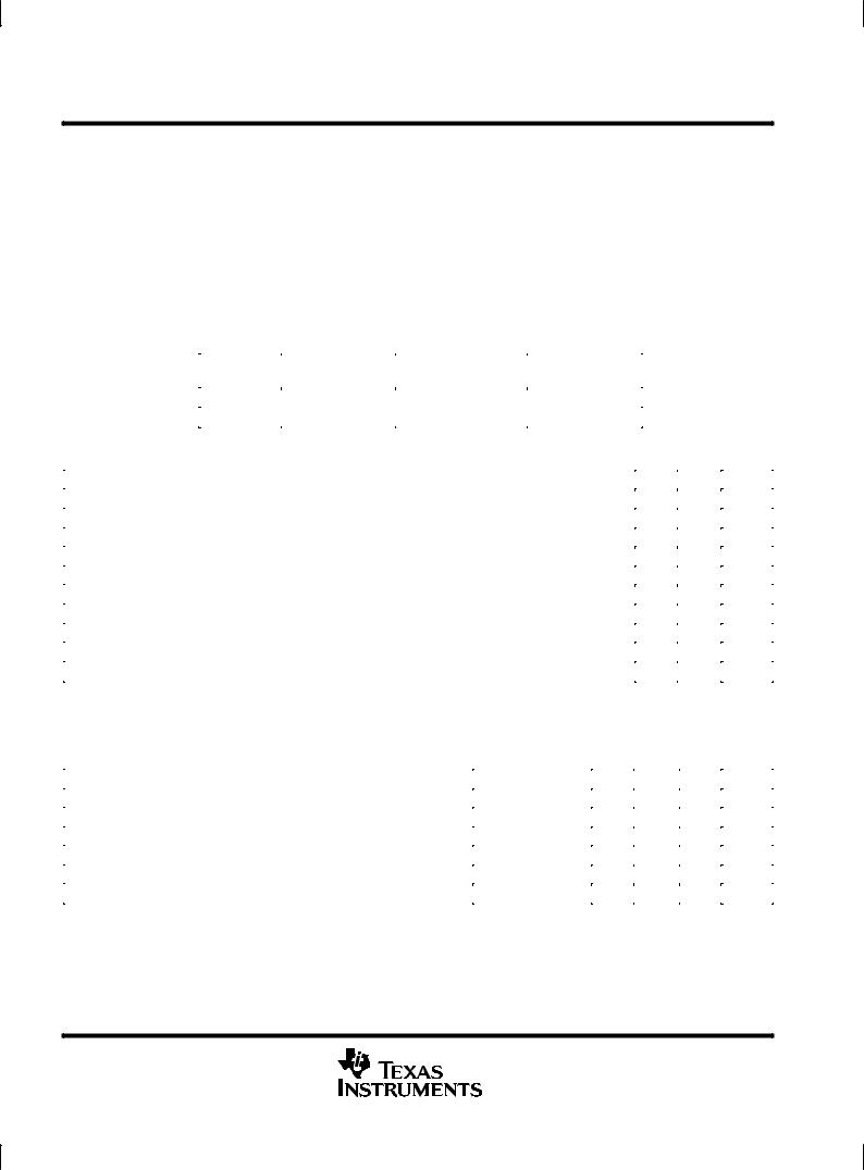
D |
Complete PWM Power Control Circuitry |
|
N OR NS PACKAGE |
|||||
D |
Completely Synchronized Operation |
|
|
|
(T0P VIEW) |
|
|
|
|
|
|
|
|
|
|
||
D Internal Undervoltage Lockout Protection |
|
CT |
|
1 |
16 |
|
REF |
|
|
|
|
||||||
D |
Wide Supply Voltage Range |
|
RT |
|
2 |
15 |
|
SCP |
|
|
|
||||||
|
|
|
|
|
3 |
14 |
|
IN+ ERROR |
|
|
|
|
|
|
|||
D |
Oscillator Frequency . . . 500 kHz Max |
AMPLIFIERERROR |
1{IN+IN± |
|
4 |
13 |
|
IN±}AMPLIFIER 2 |
|
|
|||||||
|
|
|
||||||
D Variable Dead Time Provides Control |
1 FEEDBACK |
|
5 |
12 |
|
2 FEEDBACK |
||
|
|
|||||||
|
Over Total Range |
|
|
|||||
|
1 DEAD-TIME CONTROL |
|
6 |
11 |
|
2 DEAD-TIME CONTROL |
||
|
|
|
||||||
D Internal Regulator Provides a Stable 2.5-V |
|
|
||||||
1 OUTPUT |
|
7 |
10 |
|
2 OUTPUT |
|||
|
|
|||||||
|
Reference Supply |
|
|
|||||
|
|
GND |
|
8 |
9 |
|
VCC |
|
|
|
|
|
|||||
|
|
|
|
|
||||
|
|
|
|
|
|
|
|
|
description
The TL1453C incorporates the functions required in the construction of two pulse-width-modulation control circuits on a single monolithic chip. Designed primarily for power supply control, the TL1453C contains an on-chip 2.5-V regulator, two error amplifiers, an adjustable oscillator, two dead-time comparators, undervoltage lockout circuitry, and dual common-emitter output transistor circuits.
The uncommitted output transistors provide common-emitter output capability for each controller. The internal amplifiers exhibit a common-mode voltage range from 1.05 V to 1.45 V. The dead-time control comparator has no offset unless externally altered and may be used to provide 0% to 100% dead time. The on-chip oscillator may be operated by terminating RT (pin 2) and CT (pin 1). During low-VCC conditions, the undervoltage lockout control circuit feature inhibits the output until the internal circuitry is operational.
The TL1453C is characterized for operation from ±20°C to 85°C.
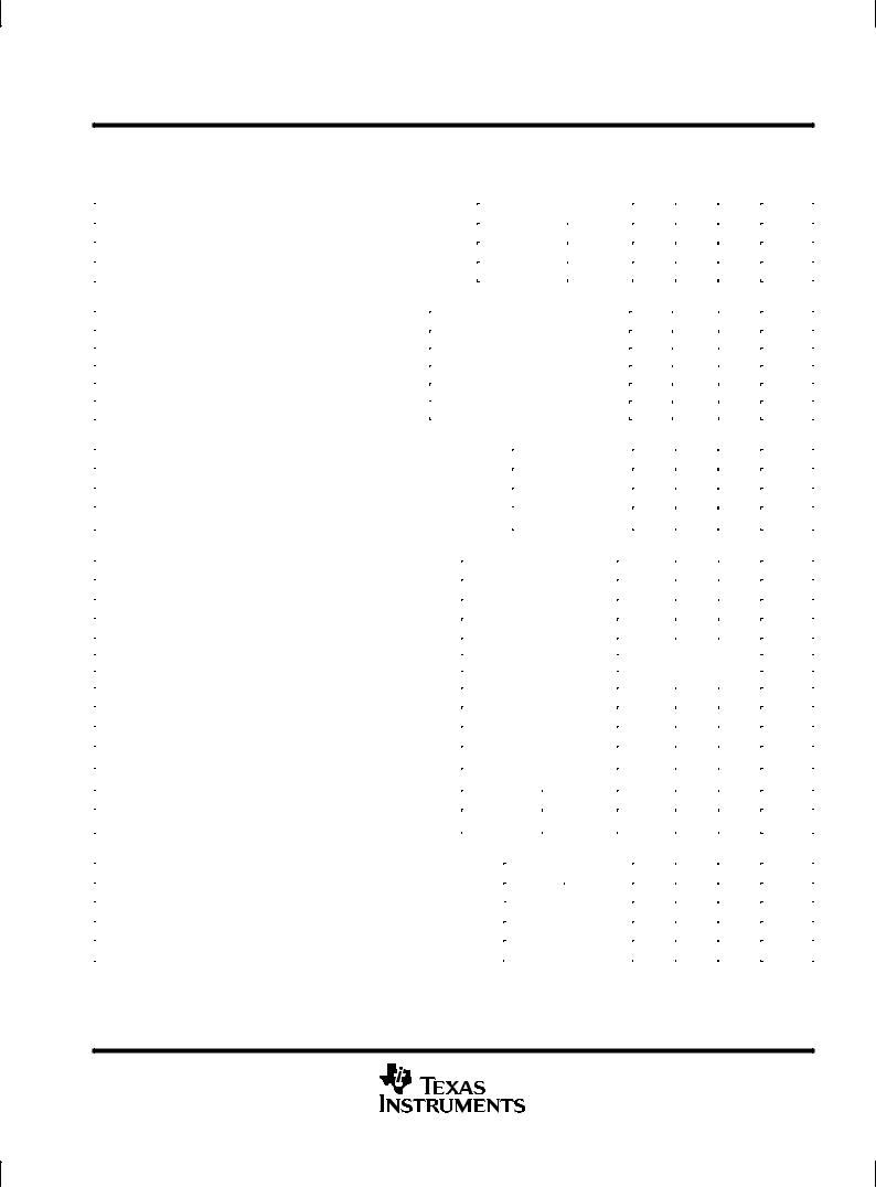
functional block diagram
|
|
VCC |
|
CT |
RT |
|
Vref = 2.5 V |
9 |
|
1 |
2 |
|
Reference |
|
Triangle |
||
REF |
16 |
|
|||
|
|
Voltage |
|
Oscillator |
|
|
|
|
2 V |
|
|
|
Error Amp.1 |
2.5 V |
1.4 V |
PWM Comparator 1 |
|
1 IN+ |
3 |
|
|
7 |
|
|
|
|
|||
|
|
|
|
|
1 OUTPUT |
1 IN± |
4 |
|
|
|
1 |
1 FEEDBACK 5 |
|
|
|
||
|
|
|
|
||
2 FEEDBACK |
12 Error Amp.2 |
|
|
|
|
2 IN+ |
14 |
|
|
|
10 |
|
|
|
|
|
2 OUTPUT |
2 IN± |
13 |
|
2.5 V |
|
|
|
|
|
|
||
|
|
|
|
2 |
|
|
|
|
|
|
|
|
|
|
2.5 V |
PWM Comparator 2 |
|
|
|
|
|
||
SCP 15 |
|
UVLO² |
|
|
|
|
|
|
|
|
8 |
|
|
|
6 |
11 |
GND |
|
|
|
|
||
² UVLO = Undervoltage Lockout Protection |
1 DEAD-TIME CONTROL |
2 DEAD-TIME CONTROL |
|||
|
|
|
|||
PRODUCTION DATA information is current as of publication date. Products conform to specifications per the terms of Texas Instruments standard warranty. Production processing does not necessarily include testing of all parameters.
Copyright 1990, Texas Instruments Incorporated
POST OFFICE BOX 655303 •DALLAS, TEXAS 75265 |
1 |
TL1453C
DUAL PULSE-WIDTH-MODULATION CONTROL CIRCUIT
SLVS039A ± FEBRUARY 1990 ± REVISED DECEMBER 1990
absolute maximum ratings over operating free-air temperature range (unless otherwise noted)
Supply voltage, VCC (see Note 1) . . . . . . . . . . . . . . . . . . . . . . . . . . . . . . . . . . . . . . . |
. . . . . . . . . . . . . . . . . . . . 41 |
V |
Amplifier input voltage . . . . . . . . . . . . . . . . . . . . . . . . . . . . . . . . . . . . . . . . . . . . . . . . . |
. . . . . . . . . . . . . . . . . . . . . 20 |
V |
Collector output voltage . . . . . . . . . . . . . . . . . . . . . . . . . . . . . . . . . . . . . . . . . . . . . . . . |
. . . . . . . . . . . . . . . . . . . . . 51 |
V |
Collector output current . . . . . . . . . . . . . . . . . . . . . . . . . . . . . . . . . . . . . . . . . . . . . . . . |
. . . . . . . . . . . . . . . . . . . 21 mA |
|
Continuous total power dissipation . . . . . . . . . . . . . . . . . . . . . . . . . . . . . . . . . . . . . |
See Dissipation Rating Table |
|
Operating free-air temperature range, TA . . . . . . . . . . . . . . . . . . . . . . . . . . . . . . . . |
. . . . . . . . . . . . ±20°C to 85°C |
|
Storage temperature range . . . . . . . . . . . . . . . . . . . . . . . . . . . . . . . . . . . . . . . . . . . . . |
. . . . . . . . . . . ±65°C to 150°C |
|
Lead temperature 1,6 mm (1/16 inch) from case for 10 seconds . . . . . . . . . . . . |
. . . . . . . . . . . . . . . . . . . 260°C |
|
NOTE 1: All voltage values are with respect to network ground terminal.
|
DISSIPATION RATING TABLE |
|
||
PACKAGE |
TA ≤ 25°C |
DERATING FACTOR |
TA = 85°C |
|
POWER RATING |
ABOVE TA = 25°C |
POWER RATING |
||
|
||||
N |
1000 mW |
8 mW/°C |
520 mW |
|
NS |
725 mW |
5.8 mW/°C |
397 mW |
|
|
|
|
|
|
recommended operating conditions
|
MIN |
MAX |
UNIT |
|
|
|
|
Supply voltage, VCC |
3.6 |
40 |
V |
Amplifier input voltage, VI |
1.05 |
1.45 |
V |
Collector output voltage, VO |
|
50 |
V |
Collector output current |
|
20 |
mA |
|
|
|
|
Current into feedback terminal |
|
45 |
μA |
|
|
|
|
Feedback resistor, RF |
100 |
|
kΩ |
Timing capacitor, CT |
150 |
15000 |
pF |
Timing resistor, RT |
5.1 |
100 |
kΩ |
Oscillator frequency |
1 |
500 |
kHz |
|
|
|
|
Operating free-air temperature, TA |
± 20 |
85 |
°C |
electrical characteristics over recommended operating free-air temperature range, VCC = 6 V, f = 200 kHz (unless otherwise noted)
reference section
PARAMETER |
TEST CONDITIONS |
MIN |
TYP² |
MAX |
UNIT |
Output voltage (pin 16) |
IO = 1 mA |
2.4 |
2.5 |
2.6 |
V |
Output voltage change with temperature |
TA = ± 20°C to 25°C |
|
± 0.1% |
±1% |
|
TA = 25°C to 85°C |
|
± 0.2% |
±1% |
|
|
|
|
|
|||
Input regulation |
VCC = 3.6 V to 40 V |
|
2 |
12.5 |
mV |
Output regulation |
IO = 0.1 mA to 1 mA |
|
1 |
7.5 |
mV |
Short-circuit output current |
VO = 0 |
3 |
10 |
30 |
mA |
² All typical values are at T = 25°C. |
|
|
|
|
|
A |
|
|
|
|
|
2 |
POST OFFICE BOX 655303 •DALLAS, TEXAS 75265 |
TL1453C
DUAL PULSE-WIDTH-MODULATION CONTROL CIRCUIT
SLVS039A ± FEBRUARY 1990 ± REVISED DECEMBER 1990
electrical characteristics over recommended operating free-air temperature range, VCC = 6 V, f = 200 kHz (unless otherwise noted) (continued)
undervoltage lockout section
PARAMETER |
TEST CONDITIONS |
MIN |
TYP² |
MAX |
UNIT |
|
Upper threshold voltage (pin 9) |
IOref = 0.1 mA, |
TA = 25°C |
|
2.72 |
V |
|
Lower threshold voltage (pin 9) |
IOref = 0.1 mA, |
TA = 25°C |
|
2.6 |
|
V |
Hysteresis (pin 9) |
IOref = 0.1 mA, |
TA = 25°C |
80 |
120 |
mV |
|
oscillator section
PARAMETER |
TEST CONDITIONS |
MIN TYP² |
MAX |
UNIT |
Frequency |
CT = 330 pF, RT = 10 kΩ |
200 |
|
kHz |
Standard deviation of frequency |
VCC, TA, RT, CT values are constant |
10% |
|
|
Frequency change with voltage |
VCC = 3.6 V to 40 V |
1% |
|
|
Frequency change with temperature |
TA = ±20°C to 25°C |
± 0.4% |
± 2% |
|
TA = 25°C to 85°C |
± 0.2% |
± 2% |
|
|
|
|
dead-time control section
PARAMETER |
TEST CONDITIONS |
MIN |
TYP² |
MAX |
UNIT |
Input bias current (pins 6 and 11) |
|
|
|
1 |
μA |
|
|
|
|
|
|
Input threshold voltage at f = 10kHz (pins 6 and 11) |
Zero duty cycle |
|
2.05 |
2.25 |
V |
|
|
|
|
||
Maximum duty cycle |
1.2 |
1.45 |
|
||
|
|
|
|||
|
|
|
|
|
|
error-amplifier section
PARAMETER |
TEST CONDITIONS |
MIN |
TYP² |
MAX |
UNIT |
|
Input offset voltage |
VO (pins 5 and 12) = 1.25 V |
|
|
± 6 |
mV |
|
Input offset current |
VO (pins 5 and 12) = 1.25 V |
|
|
±100 |
nA |
|
Input bias current |
VO (pins 5 and 12) = 1.25 V |
|
160 |
500 |
nA |
|
|
|
|
1.05 |
|
|
|
Common-mode input voltage range |
VCC = 3.6 V to 40 V |
to |
|
|
V |
|
|
|
|
1.45 |
|
|
|
|
|
|
|
|
|
|
Open-loop voltage amplification |
RF = 200 kΩ |
|
70 |
80 |
|
dB |
Unity-gain bandwidth |
|
|
|
1.5 |
|
MHz |
|
|
|
|
|
|
|
Common-mode rejection ratio |
|
|
60 |
80 |
|
dB |
|
|
|
|
|
|
|
Positive output voltage swing |
|
|
Vref ± 0.1 |
|
|
V |
Negative output voltage swing |
|
|
|
|
1 |
V |
|
|
|
|
|
|
|
Output (sink) current (pins 5 and 12) |
VID = ± 0.1 V, |
VO = 1.25 V |
0.5 |
1.6 |
|
mA |
Output (source) current (pins 5 and 12) |
VID = 0.1 V, |
VO = 1.25 V |
± 45 |
± 70 |
|
μA |
output section
PARAMETER |
TEST CONDITIONS |
MIN TYP² |
MAX |
UNIT |
Collector off-state current |
VCC = 0, VO = 50 V |
|
10 |
μA |
VO = 50 V |
|
10 |
||
|
|
|
||
Output saturation voltage |
IO = 10 mA |
1.2 |
2 |
V |
Short-circuit output current |
VO = 6 V |
90 |
|
mA |
² All typical values are at T = 25°C. |
|
|
|
|
A |
|
|
|
|
POST OFFICE BOX 655303 •DALLAS, TEXAS 75265 |
3 |
 Loading...