


Texas Instruments TLC32045EFN, TLC32045CN, TLC32045CFN, TLC32044MJB, TLC32044MJ Datasheet
...TLC32044C, TLC32044E, TLC32044I, TLC32044M, TLC32045C, TLC32045I VOICE-BAND ANALOG INTERFACE CIRCUITS
SLAS017F ± MARCH 1988 ± REVISED MAY 1995
D14-Bit Dynamic Range ADC and DAC
D2's Complement Format
DVariable ADC and DAC Sampling Rate Up to 19,200 Samples per Second
DSwitched-Capacitor Antialiasing Input Filter and Output-Reconstruction Filter
DSerial Port for Direct Interface to TMS(SMJ)320C17, TMS(SMJ)32020, TMS(SMJ)320C25,
and TMS320C30 Digital Signal Processors
DSynchronous or Asynchronous ADC and DAC Conversion Rates With Programmable Incremental ADC and DAC Conversion Timing Adjustments
DSerial Port Interface to SN74(54)299 Serial-to-Parallel Shift Register for Parallel Interface to TMS(SMJ)32010, TMS(SMJ)320C15, or Other Digital Processors
J² OR N PACKAGE
(TOP VIEW)
|
|
|
NU |
|
1 |
28 |
NU |
||
|
|
|
|
||||||
|
|
|
|
|
|
|
|
|
NU |
|
RESET |
2 |
27 |
||||||
|
|
|
|
||||||
|
|
|
|
|
|
|
|
|
IN+ |
|
|
EODR |
3 |
26 |
|||||
|
|
|
|
||||||
|
|
|
|
|
|
|
|
IN± |
|
|
|
|
FSR |
4 |
25 |
||||
|
|
|
|
|
|
||||
|
|
|
DR |
|
5 |
24 |
AUX IN+ |
||
|
|
|
|
||||||
MSTR CLK |
|
6 |
23 |
AUX IN± |
|||||
|
|||||||||
|
|
|
VDD |
|
7 |
22 |
OUT+ |
||
|
|
|
|
||||||
|
|
|
|
|
|
||||
|
|
|
REF |
|
8 |
21 |
OUT± |
||
DGTL GND |
|
9 |
20 |
VCC + |
|||||
|
|||||||||
|
10 |
|
|||||||
SHIFT CLK |
|
19 |
VCC ± |
||||||
|
11 |
18 |
|||||||
|
|
EODX |
|
|
ANLG GND |
||||
|
|
|
DX |
|
12 |
17 |
ANLG GND |
||
|
|
|
|
||||||
|
|
|
|
|
|
|
13 |
16 |
NU |
WORD/BYTE |
|
|
|||||||
|
|
|
FSX |
|
|
|
14 |
15 |
NU |
|
|
|
|
|
|
|
|
|
|
² Refer to the mechanical data for the JT package.
FK OR FN PACKAGE
DInternal Reference for Normal Operation and External Purposes, or Can Be Overridden by External Reference
DCMOS Technology
description
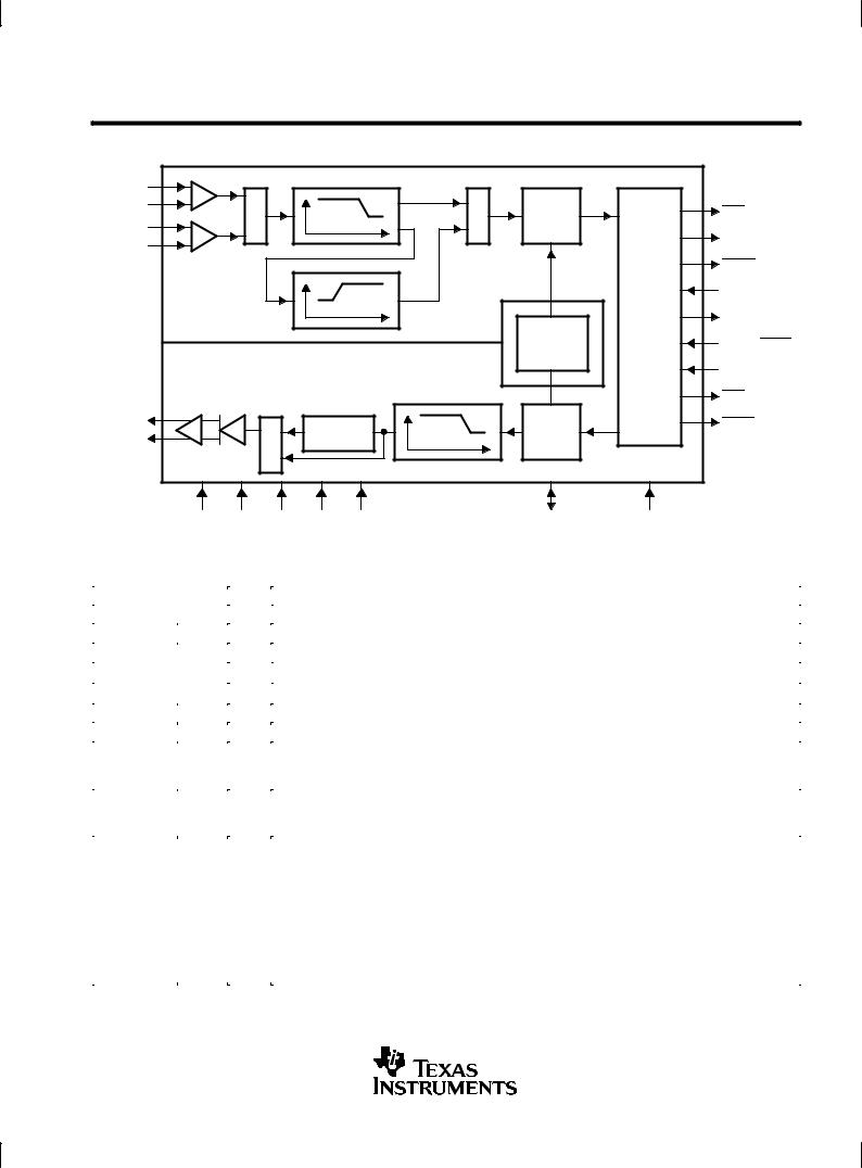
The TLC32044 and TLC32045 are complete analog-to-digital and digital-to-analog input and output systems on single monolithic CMOS chips. The TLC32044 and TLC32045 integrate a bandpass switched-capacitor antialiasing input filter, a 14-bit-resolution A/D converter, four microprocessor-compatible serial port modes, a 14-bit-resolution D/A converter, and a low-pass switched-capacitor output-reconstruction filter. The devices offer numerous combinations of master clock input frequencies and conversion/ sampling rates, which can be changed via digital processor control.
(TOP VIEW)
|
FSR |
EODR |
RESET |
NU |
NU |
NU |
IN + |
|
DR |
4 |
3 |
2 |
1 |
28 |
27 26 |
IN± |
|
5 |
|
|
|
|
|
25 |
||
MSTR CLK |
6 |
|
|
|
|
|
24 |
AUX IN+ |
VDD |
7 |
|
|
|
|
|
23 |
AUX IN± |
REF |
8 |
|
|
|
|
|
22 |
OUT+ |
DGTL GND |
9 |
|
|
|
|
|
21 |
OUT± |
SHIFT CLK |
10 |
|
|
|
|
|
20 |
VCC + |
EODX |
11 |
|
|
|
|
|
19 |
VCC ± |
|
12 13 14 15 16 17 18 |
|
||||||
|
DX |
WORD/BYTE |
FSX |
NU |
NU |
ANLG GND |
ANLG GND |
|
NU ± Nonusable; no external connection should be made to these terminals (see Table 2).
Please be aware that an important notice concerning availability, standard warranty, and use in critical applications of Texas Instruments semiconductor products and disclaimers thereto appears at the end of this data sheet.
PRODUCTION DATA information is current as of publication date. Products conform to specifications per the terms of Texas Instruments standard warranty. Production processing does not necessarily include testing of all parameters.
Copyright 1995, Texas Instruments Incorporated
POST OFFICE BOX 655303 •DALLAS, TEXAS 75265 |
1 |
TLC32044C, TLC32044E, TLC32044I, TLC32044M, TLC32045C, TLC32045I VOICE-BAND ANALOG INTERFACE CIRCUITS
SLAS017F ± MARCH 1988 ± REVISED MAY 1995
AVAILABLE OPTIONS
|
|
PACKAGE |
|
||
|
|
|
|
|
|
TA |
PLASTIC CHIP |
PLASTIC DIP |
CERAMIC DIP |
CHIP CARRIER |
|
CARRIER |
|||||
|
(N) |
(J) |
(FK) |
||
|
(FN) |
||||
|
|
|
|
||
|
|
|
|
|
|
0°C to 70°C |
TLC32044CFN |
TLC32044CN |
|
|
|
|
|
|
|
||
TLC32045CFN |
TLC32045CN |
|
|
||
|
|
|
|||
|
|
|
|
|
|
± 20°C to 85°C |
TLC32044EFN |
|
|
|
|
|
|
|
|
|
|
±40°C to 85°C |
|
TLC32044IN |
|
|
|
|
|
|
|
||
|
TLC32045IN |
|
|
||
|
|
|
|
||
|
|
|
|
|
|
± 55°C to 125°C |
|
|
TLC32044MJ |
TLC32044MFK |
|
|
|
|
|
|
|
description (continued)
Typical applications for the TLC32044 and TLC32045 include speech encryption for digital transmission, speech recognition/ storage systems, speech synthesis, modems (7.2-, 8-, 9.6-, 14.4-, and 19.2-kHz sampling rate), analog interface for digital signal processors (DSPs), industrial process control, biomedical instrumentation, acoustical signal processing, spectral analysis, data acquisition, and instrumentation recorders. Four serial modes, which allow direct interface to the TMS(SMJ)320C17, TMS(SMJ)32020, TMS(SMJ)320C25, and TMS(SMJ)320C30 digital signal processors, are provided. Also, when the transmit and receive sections of the analog interface circuit (AIC) are operating synchronously, it will interface to two SN74(54)299 serial-to-parallel shift registers. These serial-to-parallel shift registers can then interface in parallel to the TMS(SMJ)32010, TMS(SMJ)320C15, and other digital signal processors, or external FIFO circuitry. Output data pulses are emitted to inform the processor that data transmission is complete or to allow the DSP to differentiate between two transmitted bytes. A flexible control scheme is provided so that the functions of the TLC32044 or TLC32045 can be selected and adjusted coincidentally with signal processing via software control.
The antialiasing input filter comprises eighth-order and fourth-order CC-type (Chebyshev/elliptic transitional) low-pass and high-pass filters, respectively. The input filter is implemented in switched-capacitor technology and is preceded by a continuous time filter to eliminate any possibility of aliasing caused by sampled data filtering. When only low-pass filtering is desired, the high-pass filter can be switched out of the signal path. A selectable, auxiliary, differential analog input is provided for applications where more than one analog input is required.
The A/D and D/A architectures ensure no missing codes and monotonic operation. An internal voltage reference is provided to ease the design task and to provide complete control over the performance of the TLC32044 or TLC32045. The internal voltage reference is brought out to a terminal and is available to the designer. Separate analog and digital voltage supplies and grounds are provided to minimize noise and ensure a wide dynamic range. Also, the analog circuit path contains only differential circuitry to keep noise to an absolute minimum. The only exception is the DAC sample and hold, which utilizes pseudo-differential circuitry.
The output-reconstruction filter is an eighth-order CC-type (Chebyshev/elliptic transitional low-pass filter) followed by a second-order (sin x)/x correction filter and is implemented in switched-capacitor technology. This filter is followed by a continuous-time filter to eliminate images of the digitally encoded signal. The on-board (sin x)/x correction filter can be switched out of the signal path using digital signal processor control, if desired.
The TLC32044C and TLC32045C are characterized for operation from 0°C to 70°C. The TLC32044E is characterized for operation from ±20°C to 85°C. The TLC32044I and TLC32045I are characterized for operation from ±40°C to 85°C. The TLC32044M is characterized for operation from ±55°C to 125°C.
2 |
POST OFFICE BOX 655303 •DALLAS, TEXAS 75265 |
TLC32044C, TLC32044E, TLC32044I, TLC32044M, TLC32045C, TLC32045I VOICE-BAND ANALOG INTERFACE CIRCUITS
|
|
|
|
|
SLAS017F ± MARCH 1988 ± REVISED MAY 1995 |
|
functional block diagram |
|
|
|
|
|
|
IN + |
|
Filter |
|
|
|
|
|
|
|
|
|
|
|
IN ± |
M |
|
M |
A/D |
SERIAL |
FSR |
|
U |
|
U |
|||
AUX IN + |
|
PORT |
||||
X |
|
X |
|
|
||
AUX IN ± |
|
|
|
DR |
||
|
|
|
|
|
||
|
|
|
|
|
|
|
|
|
|
Receive Section |
|
EODR |
|
|
|
|
|
|
|
MSTER CLK |
|
|
|
|
Internal |
|
SHIFT CLK |
|
|
|
|
|
|
|
|
|
|
|
Voltage |
|
WORD/BYTE |
|
|
|
|
Reference |
|
|
|
|
|
|
|
|
DX |
|
|
|
Filter |
|
|
FSX |
|
|
|
|
|
|
|
OUT + |
M |
sin x/x |
|
D/A |
|
EODX |
OUT ± |
|
|
||||
Correction |
|
|
|
|||
U |
|
|
|
|
||
|
|
|
|
|
|
|
|
X |
|
Transmit Section |
|
|
|
|
|
|
|
|
||
VCC + VCC ± ANLG |
DTGL |
VDD |
REF |
RESET |
GND |
GND |
(Digital) |
|
|
|
|
|
|
|
Terminal Functions |
|
||
|
|
|
|
|
|
|
|
|
|
TERMINAL |
I/O |
|
DESCRIPTION |
|
|||
|
NAME |
NO. |
|
|
||||
|
|
|
|
|
|
|||
|
|
|
|
|
|
|
|
|
|
ANLG GND |
17,18 |
|
Analog ground return for all internal analog circuits. Not internally connected to DGTL GND. |
|
|||
|
|
|
|
|
|
|
|
|
|
AUX IN + |
24 |
I |
Noninverting auxiliary analog input stage. AUX IN + can be switched into the bandpass filter and A/D |
|
|||
|
|
|
|
|
converter path via software control. If the appropriate bit in the control register is a 1, the auxiliary inputs |
|
||
|
|
|
|
|
will replace the IN + and IN ± inputs. If the bit is a 0, the IN + and IN ± inputs will be used (see the AIC DX |
|
||
|
|
|
|
|
data word format section). |
|
||
|
|
|
|
|
|
|
|
|
|
AUX IN ± |
23 |
I |
Inverting auxiliary analog input (see the above AUX IN + description). |
|
|||
|
|
|
|
|
|
|
|
|
|
DGTL GND |
9 |
|
Digital ground for all internal logic circuits. Not internally connected to ANLG GND. |
|
|||
|
|
|
|
|
|
|
|
|
|
DR |
5 |
O |
Data receive. DR is used to transmit the ADC output bits from the AIC to the TMS320 (SMJ320) serial port. |
|
|||
|
|
|
|
|
This transmission of bits from the AIC to the TMS320 (SMJ320) serial port is synchronized with the SHIFT |
|
||
|
|
|
|
|
CLK signal. |
|
||
|
|
|
|
|
|
|
|
|
|
DX |
12 |
I |
Data transmit. DX is used to receive the DAC input bits and timing and control information from the TMS320 |
|
|||
|
|
|
|
|
(SMJ320). This serial transmission from the TMS320 (SMJ320) serial port to the AIC is synchronized with |
|
||
|
|
|
|
|
the SHIFT CLK signal. |
|
||
|
|
|
|
|
|
|
|
|
|
|
|
3 |
O |
|
|
description and Serial Port Timing diagram.) During the |
|
|
EODR |
|
End of data receive. (See the WORD/BYTE |
|
||||
|
|
|
|
|
word-mode timing, EODR is a low-going pulse that occurs immediately after the 16 bits of A/D information |
|
||
|
|
|
|
|
have been transmitted from the AIC to the TMS320 (SMJ320) serial port. EODR can be used to interrupt |
|
||
|
|
|
|
|
a microprocessor upon completion of serial communications. Also, EODR can be used to strobe and enable |
|
||
|
|
|
|
|
external serial-to-parallel shift registers, latches, or external FIFO RAM, and to facilitate parallel data bus |
|
||
|
|
|
|
|
communications between the AIC and the serial-to-parallel shift registers. During the byte-mode timing, |
|
||
|
|
|
|
|
EODR goes low after the first byte has been transmitted from the AIC to the TMS320 (SMJ320) serial port |
|
||
|
|
|
|
|
and is kept low until the second byte has been transmitted. The DSP can use this low-going signal to |
|
||
|
|
|
|
|
differentiate between the two bytes as to which is first and which is second. EODR does not occur after |
|
||
|
|
|
|
|
secondary communication. |
|
||
|
|
|
|
|
|
|
|
|
|
|
|
|
|
|
|
|
|
|
|
|
|
|
|
|
|
|
POST OFFICE BOX 655303 •DALLAS, TEXAS 75265 |
3 |
TLC32044C, TLC32044E, TLC32044I, TLC32044M, TLC32045C, TLC32045I VOICE-BAND ANALOG INTERFACE CIRCUITS
SLAS017F ± MARCH 1988 ± REVISED MAY 1995
|
|
|
|
|
|
|
|
Terminal Functions (continued) |
||||||
|
|
|
|
|
|
|
|
|
|
|
|
|
|
|
|
|
|
|
TERMINAL |
|
I/O |
|
|
|
DESCRIPTION |
||||
|
NAME |
NO. |
|
|
|
|||||||||
|
|
|
|
|
|
|
|
|
||||||
|
|
|
|
|
|
|
|
|
|
|
|
|||
|
|
|
|
|
|
11 |
O |
|
|
|
|
|
|
|
|
EODX |
|
|
End of data transmit. (See the WORD/BYTE |
description and Serial Port Timing diagram.) During the |
|||||||||
|
|
|
|
|
|
|
|
word-mode timing, EODX is a low-going pulse that occurs immediately after the 16 bits of D/A converter |
||||||
|
|
|
|
|
|
|
|
and control or register information have been transmitted from the TMS320 (SMJ320) serial port to the AIC. |
||||||
|
|
|
|
|
|
|
|
EODX can be used to interrupt a microprocessor upon the completion of serial communications. Also, |
||||||
|
|
|
|
|
|
|
|
EODX can be used to strobe and enable external serial-to-parallel shift registers, latches, or an external |
||||||
|
|
|
|
|
|
|
|
FIFO RAM, and to facilitate parallel data-bus communications between the AIC and the serial-to-parallel |
||||||
|
|
|
|
|
|
|
|
shift registers. During the byte-mode timing, EODX goes low after the first byte has been transmitted from |
||||||
|
|
|
|
|
|
|
|
the TMS320 (SMJ320) serial port to the AIC and is kept low until the second byte has been transmitted. The |
||||||
|
|
|
|
|
|
|
|
DSP can use this low-going signal to differentiate between the two bytes as to which is first and which is |
||||||
|
|
|
|
|
|
|
|
second. |
||||||
|
|
|
|
|
|
|
|
|
||||||
|
|
|
|
|
|
4 |
O |
|
|
|
|
|
|
|
|
FSR |
|
|
Frame sync receive. In the serial transmission modes, which are described in the WORD/BYTE |
description, |
|||||||||
|
|
|
|
|
|
|
|
FSR is held low during bit transmission. When FSR goes low, the TMS320 (SMJ320) serial port begins |
||||||
|
|
|
|
|
|
|
|
receiving bits from the AIC via DR of the AIC. The most significant DR bit is present on DR before FSR goes |
||||||
|
|
|
|
|
|
|
|
low. (See Serial Port Timing and Internal Timing Configuration diagrams.) FSR does not occur after |
||||||
|
|
|
|
|
|
|
|
secondary communications. |
||||||
|
|
|
|
|
|
|
|
|||||||
|
|
|
|
|
|
14 |
O |
Frame sync transmit. When FSX goes low, the TMS320 (SMJ320) serial port begins transmitting bits to the |
||||||
|
FSX |
|
|
|||||||||||
|
|
|
|
|
|
|
|
AIC via DX of the AIC. In all serial transmission modes, which are described in the WORD/BYTE description, |
||||||
|
|
|
|
|
|
|
|
FSX is held low during bit transmission (see Serial Port Timing and Internal Timing Configuration diagrams). |
||||||
|
|
|
|
|
|
|
|
|||||||
|
IN + |
26 |
I |
Noninverting input to analog input amplifier stage |
||||||||||
|
|
|
|
|
|
|
|
|||||||
|
IN ± |
25 |
I |
Inverting input to analog input amplifier stage |
||||||||||
|
|
|
|
|
|
|
|
|||||||
|
MSTR CLK |
6 |
I |
Master clock. MSTR CLK is used to derive all the key logic signals of the AIC, such as the shift clock, the |
||||||||||
|
|
|
|
|
|
|
|
switched-capacitor filter clocks, and the A/D and D/A timing signals. The Internal Timing Configuration |
||||||
|
|
|
|
|
|
|
|
diagram shows how these key signals are derived. The frequencies of these key signals are synchronous |
||||||
|
|
|
|
|
|
|
|
submultiples of the master clock frequency to eliminate unwanted aliasing when the sampled analog signals |
||||||
|
|
|
|
|
|
|
|
are transferred between the switched-capacitor filters and the A/D and D/A converters (see the Internal |
||||||
|
|
|
|
|
|
|
|
Timing Configuration diagram). |
||||||
|
|
|
|
|
|
|
|
|||||||
|
OUT + |
22 |
O |
Noninverting output of analog output power amplifier. OUT+ can drive transformer hybrids or |
||||||||||
|
|
|
|
|
|
|
|
high-impedance loads directly in either a differential or a single-ended configuration. |
||||||
|
|
|
|
|
|
|
|
|||||||
|
OUT ± |
21 |
O |
Inverting output of analog output power amplifier. OUT± is functionally identical with and complementary |
||||||||||
|
|
|
|
|
|
|
|
to OUT +. |
||||||
|
|
|
|
|
|
|
|
|||||||
|
REF |
8 |
I/O |
Internal voltage reference. An internal reference voltage is brought out on REF. An external voltage |
||||||||||
|
|
|
|
|
|
|
|
reference can also be applied to REF. |
||||||
|
|
|
|
|
|
|
||||||||
|
|
|
|
|
|
2 |
I |
Reset function. |
|
is provided to initialize the TA, TA', TB, RA, RA', RB, and control registers. A reset |
||||
|
RESET |
|
RESET |
|||||||||||
|
|
|
|
|
|
|
|
initiates serial communications between the AIC and DSP. A reset initializes all AIC registers including the |
||||||
|
|
|
|
|
|
|
|
control register. After a negative-going pulse on RESET, the AIC registers are initialized to provide an 8-khz |
||||||
|
|
|
|
|
|
|
|
data conversion rate for a 5.184-MHz master clock input signal. The conversion rate adjust registers, TA' |
||||||
|
|
|
|
|
|
|
|
and RA', are reset to 1. The control register bits are reset as follows (see AIC DX data word format section): |
||||||
|
|
|
|
|
|
|
|
d9 = 1, d7 = 1, d6 = 1, d5 = 1, d4 = 0, d3 = 0, d2 = 1. |
||||||
|
|
|
|
|
|
|
|
This initialization allows normal serial-port communication to occur between the AIC and DSP. |
||||||
|
|
|
|
|
||||||||||
|
SHIFT CLK |
10 |
O |
Shift clock. SHIFT CLK is obtained by dividing the master clock signal frequency by four. SHIFT CLK is used |
||||||||||
|
|
|
|
|
|
|
|
to clock the serial data transfers of the AIC, described in the WORD/BYTE description below (see the Serial |
||||||
|
|
|
|
|
|
|
|
Port Timing and Internal Timing Configuration diagrams). |
||||||
|
|
|
|
|
||||||||||
|
VDD |
7 |
|
Digital supply voltage, 5 V ± 5% |
||||||||||
|
VCC + |
20 |
|
Positive analog supply voltage, 5 V ± 5% |
||||||||||
|
VCC ± |
19 |
|
Negative analog supply voltage, ± 5 V ± 5% |
||||||||||
4 |
POST OFFICE BOX 655303 •DALLAS, TEXAS 75265 |

TLC32044C, TLC32044E, TLC32044I, TLC32044M, TLC32045C, TLC32045I VOICE-BAND ANALOG INTERFACE CIRCUITS
|
|
|
|
|
|
|
SLAS017F ± MARCH 1988 ± REVISED MAY 1995 |
||
|
|
|
|
|
|
|
|
|
|
|
|
|
|
|
Terminal Functions (continued) |
||||
|
|
|
|
|
|
|
|
|
|
TERMINAL |
|
I/O |
|
DESCRIPTION |
|||||
NAME |
NO. |
|
|||||||
|
|
|
|
|
|
||||
|
|
|
|
|
|
||||
|
|
|
13 |
I |
|
|
|
|
|
WORD/BYTE |
|
Used in conjunction with a bit in the control register, WORD/BYTE is used to establish one of four serial |
|||||||
|
|
|
|
|
modes. These four serial modes are described below. |
||||
|
|
|
|
|
AIC transmit and receive sections are operated asynchronously. |
||||
|
|
|
|
|
The following description applies when the AIC is configured to have asynchronous transmit and receive |
||||
|
|
|
|
|
sections. If the appropriate data bit in the control register is a 0 (see the AIC DX data word format section), |
||||
|
|
|
|
|
the transmit and receive sections are asynchronous. |
||||
|
|
|
|
|
L Serial |
port directly interfaces with the serial port of the DSP and communicates in two |
|||
|
|
|
|
|
8-bit bytes. The operation sequence is as follows (see Serial Port Timing diagrams). |
||||
|
|
|
|
|
1. |
FSX or FSR is brought low. |
|||
|
|
|
|
|
2. |
One 8-bit byte is transmitted or one 8-bit byte is received. |
|||
|
|
|
|
|
3. |
EODX or EODR is brought low. |
|||
|
|
|
|
|
4. |
FSX or FSR emits a positive frame-sync pulse that is four shift clock cycles wide. |
|||
|
|
|
|
|
5. |
One 8-bit byte is transmitted or one 8-bit byte is received. |
|||
|
|
|
|
|
6. |
EODX or EODR is brought high. |
|||
|
|
|
|
|
7. |
FSX or FSR is brought high. |
|||
HSerial port directly interfaces with the serial ports of the TMS(SMJ)32020, TMS(SMJ)320C25, or TMS(SMJ)320C30, and communicates in one 16-bit word. The operation sequence is as follows (see Serial Port Timing diagrams):
1.FSX or FSR is brought low.
2.One 16-bit word is transmitted or one 16-bit word is received.
3.FSX or FSR is brought high.
4.EODX or EODR emits a low-going pulse.
AIC transmit and receive sections are operated synchronously.
If the appropriate data bit in the control register is 1, the transmit and receive sections are configured to be synchronous. In this case, the bandpass switched-capacitor filter and the A/D conversion timing are derived from the TX counter A, TX counter B, and TA, TA', and TB registers, rather than the RX counter A, RX counter B, and RA, RA', and RB registers. In this case, the AIC FSX and FSR timing are identical during primary data communication; however, FSR is not asserted during secondary data communication since there is no new A/D conversion result. The synchronous operation sequences are as follows (see Serial Port Timing diagrams).
LSerial port directly interfaces with the serial port of the DSP and communicates in two 8-bit bytes. The operation sequence is as follows (see Serial Port Timing diagrams):
1.FSX and FSR are brought low.
2.One 8-bit byte is transmitted and one 8-bit byte is received.
3.EODX and EODR are brought low.
4.FSX and FSR emit positive frame-sync pulses that are four shift clock cycles wide.
5.One 8-bit byte is transmitted and one 8-bit byte is received.
6.EODX and EODR are brought high.
7.FSX and FSR are brought high.
HSerial port directly interfaces with the serial port of the TMS(SJM)32020, TMS(SMJ)320C25, or TMS320C30, and communicates in one 16-bit word. The operation sequence is as follows (see Serial Port Timing diagrams):
1.FSX and FSR are brought low.
2.One 16-bit word is transmitted and one 16-bit word is received.
3.FSX and FSR are brought high.
4.EODX or EODR emit low-going pulses.
Since the transmit and receive sections of the AIC are now synchronous, the AIC serial port with additional NOR and AND gates interface to two SN74(54)299 serial-to-parallel shift registers. Interfacing the AIC to the SN74(54)299 shift register allows the AIC to interface to an external FIFO RAM and facilitates parallel, data bus communications between the AIC and the digital signal processor. The operation sequence is the same as the above sequence (see Serial Port Timing diagrams).
POST OFFICE BOX 655303 •DALLAS, TEXAS 75265 |
5 |

TLC32044C, TLC32044E, TLC32044I, TLC32044M, TLC32045C, TLC32045I VOICE-BAND ANALOG INTERFACE CIRCUITS
SLAS017F ± MARCH 1988 ± REVISED MAY 1995
PRINCIPLES OF OPERATION
analog input
Two sets of analog inputs are provided. Normally, the IN+ and IN± input set is used; however, the auxiliary input set, AUX IN + and AUX IN±, can be used if a second input is required. Each input set can be operated in either differential or single-ended modes, since sufficient common-mode range and rejection are provided. The gain for the IN +, IN±, AUX IN +, and AUX IN± inputs can be programmed to be either 1, 2, or 4 (see Table 2). Either input circuit can be selected via software control. It is important to note that a wide dynamic range is assured by the differential internal analog architecture and by the separate analog and digital voltage supplies and grounds.
A/D bandpass filter, A/D bandpass filter clocking, and A/D conversion timing
The A/D high-pass filter can be selected or bypassed via software control. The frequency response of this filter is presented in the following pages. This response results when the switched-capacitor filter clock frequency is 288 kHz and the A/D sample rate is 8 kHz. Several possible options can be used to attain a 288-kHz switched-capacitor filter clock. When the filter clock frequency is not 288 kHz, the low-pass filter transfer function is frequency scaled by the ratio of the actual clock frequency to 288 kHz. The ripple bandwidth and 3-dB low-frequency roll-off points of the high-pass section are 150 Hz and 100 Hz, respectively. However, the high-pass section low-frequency roll-off is frequency scaled by the ratio of the A/D sample rate to 8 kHz.
The internal timing configuration and AIC DX data word format sections of this data sheet indicate the many options for attaining a 288-kHz bandpass switched-capacitor filter clock. These sections indicate that the RX counter A can be programmed to give a 288-kHz bandpass switched-capacitor filter clock for several master clock input frequencies.
The A/D conversion rate is then attained by frequency dividing the 288-kHz bandpass switched-capacitor filter clock with the RX counter B. Unwanted aliasing is prevented because the A/D conversion rate is an integral submultiple of the bandpass switched-capacitor filter sampling rate, and the two rates are synchronously locked.
A/D converter performance specifications
Fundamental performance specifications for the A/D converter circuitry are presented in the A/D converter operating characteristics section of this data sheet. The realization of the A/D converter circuitry with switched-capacitor techniques provides an inherent sample-and-hold.
analog output
The analog output circuitry is an analog output power amplifier. Both noninverting and inverting amplifier outputs are brought out. This amplifier can drive transformer hybrids or low-impedance loads directly in either a differential or single-ended configuration.
D/A low-pass filter, D/A low-pass filter clocking, and D/A conversion timing
The frequency response of this filter is presented in the following pages. This response results when the low-pass switched-capacitor filter clock frequency is 288 kHz. Like the A/D filter, the transfer function of this filter is frequency scaled when the clock frequency is not 288 kHz. A continuous-time filter is provided on the output of the (sin x)/x correction filter to eliminate the periodic sample data signal information, which occurs at multiples of the 288-kHz switched-capacitor filter clock. The continuous time filter also greatly attenuates any switched-capacitor clock feedthrough.
6 |
POST OFFICE BOX 655303 •DALLAS, TEXAS 75265 |

TLC32044C, TLC32044E, TLC32044I, TLC32044M, TLC32045C, TLC32045I VOICE-BAND ANALOG INTERFACE CIRCUITS
SLAS017F ± MARCH 1988 ± REVISED MAY 1995
PRINCIPLES OF OPERATION
D/A low-pass filter, D/A low-pass filter clocking, and D/A conversion timing (continued)
The D/A conversion rate is attained by frequency dividing the 288-kHz switched-capacitor filter clock with TX Counter B. Unwanted aliasing is prevented because the D/A conversion rate is an integral submultiple of the switched-capacitor low-pass filter sampling rate, and the two rates are synchronously locked.
asynchronous versus synchronous operation
If the transmit section of the AIC (low-pass filter and DAC) and receive section (bandpass filter and ADC) are operated asynchronously, the low-pass and bandpass filter clocks are independently generated from the master clock signal. Also, the D/A and A/D conversion rates are independently determined. If the transmit and receive sections are operated synchronously, the low-pass filter clock drives both low-pass and bandpass filters. In synchronous operation, the A/D conversion timing is derived from, and is equal to, the D/A conversion timing (see description of the WORD/BYTE in the Terminal Functions table.)
D/A converter performance specifications
Fundamental performance specifications for the D/A converter circuitry are presented in the D/A converter operating characteristics section of the data sheet. The D/A converter has a sample-and-hold that is realized with a switched-capacitor ladder.
system frequency response correction
The (sin x)/x correction for the D/A converter zero-order sample-and-hold output can be provided by an on-board second-order (sin x)/x correction filter. This (sin x)/x correction filter can be inserted into or deleted from the signal path by digital signal processor control. When inserted, the (sin x)/x correction filter follows the switched-capacitor low-pass filter. When the TB register (see Internal Timing Configuration section) equals 36, the correction results of Figures 11 and 12 can be obtained.
The (sin x)/x correction can also be accomplished by deleting the on-board second-order correction filter and performing the (sin x)/x correction in digital signal processor software. The system frequency response can be corrected via DSP software to ± 0.1-dB accuracy to a band edge of 3000 Hz for all sampling rates. This correction is accomplished with a first-order digital correction filter, which requires only seven TMS320 (SMJ320) instruction cycles. With a 200-ns instruction cycle, seven instructions represent an overhead factor of only 1.1% and 1.3% for sampling rates of 8 and 9.6 kHz, respectively (see the (sin x)/x correction section for more details).
serial port
The serial port has four possible modes that are described in detail in the Terminal Functions table. These modes are briefly described below and in the functional description for WORD/BYTE.
•The transmit and receive sections are operated asynchronously, and the serial port interfaces directly with the DSP.
•The transmit and receive sections are operated asynchronously, and the serial port interfaces directly with the TMS(SMJ)32020, TMS(SMJ)320C25, and the TMS(SMJ)320C30.
•The transmit and receive sections are operated synchronously, and the serial port interfaces directly with the DSP.
•The transmit and receive sections are operated synchronously, and the serial port interfaces directly with the TMS(SMJ)32020, TMS(SMJ)320C25, TMS(SMJ)320C30, or two SN74(54)299 serial-to- parallel shift registers, which can then interface in parallel to the TMS(SMJ)32010, TMS(SMJ)320C15, and SMJ320E15 to any other digital signal processor or to external FIFO circuitry.
POST OFFICE BOX 655303 •DALLAS, TEXAS 75265 |
7 |

TLC32044C, TLC32044E, TLC32044I, TLC32044M, TLC32045C, TLC32045I VOICE-BAND ANALOG INTERFACE CIRCUITS
SLAS017F ± MARCH 1988 ± REVISED MAY 1995
PRINCIPLES OF OPERATION
operation of TLC32044 or TLC32045 with internal voltage reference
The internal reference eliminates the need for an external voltage reference and provides overall circuit cost reduction. Thus, the internal reference eases the design task and provides complete control over device performance. The internal reference is brought out to a terminal and is available to the designer. To keep the amount of noise on the reference signal to a minimum, an external capacitor can be connected between REF and ANLG GND.
operation of TLC32044 or TLC32045 with external voltage reference
REF can be driven from an external reference circuit. This external circuit must be capable of supplying 250 μA and must be adequately protected from noise such as crosstalk from the analog input.
reset
A reset function is provided to initiate serial communications between the AIC and DSP and to allow fast, cost-effective testing during manufacturing. The reset function initializes all AIC registers, including the control register. After a negative-going pulse on RESET, the AIC is initialized. This initialization allows normal serial port communications activity to occur between AIC and DSP (see AIC DX data word format section).
loopback
This feature allows the user to test the circuit remotely. In loopback, OUT+ and OUT± are internally connected to the IN+ and IN±. Thus, the DAC bits (d15 to d2), which are transmitted to DX, can be compared with the ADC bits (d15 to d2), which are received from DR. An ideal comparison would be that the bits on DR equal the bits on DX. However, there are some difference in these bits due to the ADC and DAC output offsets. The loopback feature is implemented with digital signal processor control by transmitting the appropriate serial port bit to the control register (see AIC DX data word format section).
8 |
POST OFFICE BOX 655303 •DALLAS, TEXAS 75265 |

TLC32044C, TLC32044E, TLC32044I, TLC32044M, TLC32045C, TLC32045I VOICE-BAND ANALOG INTERFACE CIRCUITS
SLAS017F ± MARCH 1988 ± REVISED MAY 1995
INTERNAL TIMING CONFIGURATION
MSTR CLK
5.184 MHz (1)
10.368 MHz (2)
20.736 MHz (1)
41.472 MHz (2)
XTAL |
TMS(SMJ)320 |
OSC |
DSP |
Optional External Circuitry |
||
for Full Duplex Modems |
||
|
153.6-kHz |
|
Divide |
Clock (1) |
Commercial |
|
||
|
External |
|
by 135 |
|
|
|
Front-End |
|
|
|
|
|
|
Full-Duplex |
|
|
Split-Band |
|
|
Filters² |
|
|
Divide by 4 |
|
|
|
|
SHIFT CLK |
|||
|
|
|
|
|
|
1.296 MHz (1) |
||||
|
|
|
|
|
|
|
|
|
||
|
|
|
|
|
|
|
|
|
2.592 MHz (2) |
|
TA Register |
TA' Register |
|
|
|
||||||
|
(6 bits) |
|
|
|
||||||
(5 bits) |
|
|
|
|
|
|||||
|
(2's compl) |
|
|
Low-Pass/ |
||||||
|
|
|
|
|
|
|||||
|
|
|
|
|
|
|
|
|
|
(sin x/x |
|
|
|
|
Adder/ |
|
|
|
Divide by 2 |
Correction |
|
|
|
|
|
|
|
|
Switched |
|||
|
|
|
|
|
|
|
|
|
||
|
|
|
Subtractor |
|
|
|
|
Capacitor Filter |
||
|
|
|
|
(6 bits) |
|
|
|
TB Register |
CLK = 288-kHz |
|
|
|
|
|
|
|
|
|
Square Wave |
||
|
|
|
|
|
|
|
|
(6 bits) |
||
|
|
|
|
|
|
|
|
|
||
d0, d1 = 0,0 |
|
d0, d1 = 0,1 |
TX Counter B |
|
||||||
d , d |
1 |
= 1,1³ |
|
d , d |
1 |
= 1,0³ |
|
|||
|
|
|
|
|||||||
0 |
|
|
0 |
|
|
[ TB = 40; |
7.2 kHz] |
|
||
|
|
TX Counter A |
|
|
|
D/A |
||||
|
|
|
|
|
[ TB = 36; |
8.0 kHz] |
||||
|
|
|
|
|
Conversion |
|||||
|
|
[ TA = 9 (1)] |
|
|
|
[ TB = 30; |
9.6 kHz] |
|||
|
|
|
|
|
Frequency |
|||||
|
|
[ TA = 18 (2)] |
|
|
576-kHz |
[ TB = 20; |
14.4 kHz] |
|||
|
|
|
|
|
||||||
|
|
(6 bits) |
|
|
[ TB = 15; |
19.2 kHz] |
|
|||
|
|
|
|
Pulses |
|
|||||
|
|
|
|
|
|
|
|
|
|
|
RA Register |
RA' Register |
|
|
|
||||||
|
(6 bits) |
|
|
|
||||||
(5 bits) |
|
|
|
|
|
|||||
|
(2's compl) |
|
|
|
||||||
|
|
|
|
|
|
Low-Pass |
||||
|
|
|
|
|
|
|
|
|
|
|
|
|
|
|
|
|
|
|
|
|
Switched |
|
|
|
|
Adder/ |
|
|
|
Divide by 2 |
Capacitor Filter |
|
|
|
|
|
|
|
|
|
|
CLK = 288-kHz |
|
|
|
|
Subtractor |
|
|
|
|
|||
|
|
|
|
|
|
|
Square Wave |
|||
|
|
|
|
(6 bits) |
|
|
|
|
|
|
|
|
|
|
|
|
|
RB Register |
|
||
|
|
|
|
|
|
|
|
|
||
|
|
|
|
|
|
|
|
(6 bits) |
|
|
d0, d1 = 0,0 |
|
d0, d1 = 0,1 |
RX Counter B |
A/D |
||||||
d , d |
1 |
= 1,1³ |
|
d , d |
1 |
= 1,0³ |
Conversion |
|||
0 |
|
|
0 |
|
|
[RB = 40; |
7.2 kHz] |
Frequency/ |
||
|
|
RX Counter A |
|
|
|
|||||
|
|
|
|
|
[RB = 36; |
8.0 kHz] |
High-Pass |
|||
|
|
[RA = 9 (1)] |
|
|
|
[RB = 30; |
9.6 kHz] |
Switched |
||
|
|
[RA = 18 (2)] |
|
|
576-kHz |
[RB = 20; |
14.4 kHz] |
Capacitor |
||
|
|
(6 bits) |
|
|
||||||
|
|
|
|
Pulses |
[RB = 15; |
19.2 kHz] |
Filter CLK |
|||
|
|
|
|
|
|
|
||||
² Split-band filtering can alternatively be performed after the analog input function via software in the TMS(SMJ)320. ³ These control bits are described in the AIC DX data word format section.
NOTE: Frequency 1 (20.736 MHz) is used to show how 153.6 kHz (for a commercially available modem split-band filter clock), popular speech and modem sampling signal frequencies, and an internal 288-kHz switched-capacitor filter clock can be derived synchronously and as submultiples of the crystal oscillator frequency. Since these derived frequencies are synchronous submultiples of the crystal frequency, aliasing does not occur as the sampled analog signal passes between the analog converter and switched-capacitor filter stages. Frequency 2 (41.472 MHz) is used to show that the AIC can work with high-frequency signals, which are used by high-speed digital signal processors.
POST OFFICE BOX 655303 •DALLAS, TEXAS 75265 |
9 |

TLC32044C, TLC32044E, TLC32044I, TLC32044M, TLC32045C, TLC32045I VOICE-BAND ANALOG INTERFACE CIRCUITS
SLAS017F ± MARCH 1988 ± REVISED MAY 1995
explanation of internal timing configuration
All of the internal timing of the AIC is derived from the high-frequency clock signal that drives the master clock input. The shift clock signal, which strobes the serial port data between the AIC and DSP, is derived by dividing the master clock input signal frequency by four.
Low-pass: |
|
|
SCF Clock Frequency (D A or A D path) + |
Master Clock Frequency |
|
|
||
2 Contents of Counter A |
|
|
Conversion Frequency + SCF Clock Frequency (D A or A D path)
Contents of Counter B
High-pass:
SCF Clock Frequency (A D Path) + A D Conversion Frequency
Shift Clock Frequency + Master Clock Frequency
4
TX counter A and TX counter B, which are driven by the master clock, determine the D/A conversion timing. Similarly, RX counter A and RX counter B determine the A/D conversion timing. In order for the low-pass switched-capacitor filter in the D/A path to meet its transfer function specifications, the frequency of its clock input must be 288 kHz. If the clock frequency is not 288 kHz, the filter transfer function frequencies are frequency-scaled by the ratios of the clock frequency to 288 kHz. Thus, to obtain the specified filter response, the combination of master clock frequency and TX counter A and RX counter A values must yield a 288-kHz switched-capacitor clock signal. This 288-kHz clock signal can then be divided by the TX counter B to establish the D/A conversion timing.
The transfer function of the bandpass switched-capacitor filter in the A/D path is a composite of its high-pass and low-pass section transfer functions. The high-frequency roll-off of the low-pass section meets the bandpass filter transfer function specification when the low-pass section SCF is 288 kHz. Otherwise, the high-frequency roll-off will be frequency-scaled by the ratio of the high-pass section's SCF clock to 288 kHz. The low-frequency roll-off of the high-pass section meets the bandpass filter transfer function specification when the A/D conversion rate is 8 kHz. Otherwise, the low-frequency roll-off of the high-pass section is frequency-scaled by the ratio of the A/D conversion rate to 8 kHz.
TX counter A and TX counter B are reloaded every D/A conversion period, while RX counter A and RX counter B are reloaded every A/D conversion period. The TX counter B and RX counter B are loaded with the values in the TB and RB registers, respectively. Via software control, the TX counter A can be loaded with either the TA register, the TA register less the TA' register, or the TA register plus the TA' register. By selecting the TA register less the TA' register option, the upcoming conversion timing occurs earlier by an amount of time that equals TA' times the signal period of the master clock. By selecting the TA register plus the TA' register option, the upcoming conversion timing occurs later by an amount of time that equals TA' times the signal period of the master clock. The D/A conversion timing can be advanced or retarded. An identical ability to alter the A/D conversion timing is provided. In this case, however, the RX counter A can be programmed via software control with the RA register, the RA register less the RA' register, or the RA register plus the RA' register.
The ability to advance or retard conversion timing is particularly useful for modem applications. This feature allows controlled changes in the A/D and D/A conversion timing. This feature can be used to enhance signal-to-noise performance, to perform frequency-tracking functions, and to generate nonstandard modem frequencies.
10 |
POST OFFICE BOX 655303 •DALLAS, TEXAS 75265 |
TLC32044C, TLC32044E, TLC32044I, TLC32044M, TLC32045C, TLC32045I VOICE-BAND ANALOG INTERFACE CIRCUITS
SLAS017F ± MARCH 1988 ± REVISED MAY 1995
explanation of internal timing configuration (continued)
If the transmit and receive sections are configured to be synchronous (see WORD/BYTE description), then both the low-pass and bandpass switched-capacitor filter clocks are derived from TX counter A. Also, both the D/A and A/D conversion timing are derived from the TX counter A and TX counter B. When the transmit and receive sections are configured to be synchronous, the RX counter A, RX counter B, RA register, RA' register, and RB registers are not used.
AIC DR or DX word bit pattern
A/D or D/A MSB, |
|
|
|
|
|
|
|
|
|
|
|
|
|
|
|
|
||||
1st bit sent |
|
|
|
|
1st bit sent of 2nd byte |
|
A/D or D/A LSB |
|
||||||||||||
|
|
|
|
|
|
|
|
|
|
|
|
|
|
|
|
|
|
|
|
|
|
d15 |
d14 |
|
d13 |
d12 |
d11 |
d10 |
d9 |
d8 |
d7 |
d6 |
d5 |
d4 |
d3 |
d2 |
d1 |
d0 |
|||
|
|
|
|
|
|
|
|
|
|
|
|
|
|
|
|
|
|
|
|
|
AIC DX data word format section
d15 |
d14 |
d13 |
d12 |
d11 |
d10 |
d9 |
d8 |
d7 |
d6 |
d5 |
d4 |
d3 |
d2 |
d1 |
d0 |
Comments |
|
|
|
|
|
|
|
|
|
|
|
|
|
|
|
|
|
primary DX serial communication protocol |
|
|
|
|
|
|
|
|
|
|||||||
|
|
|
|
|
|
|
|
|
|
|
|
|
|
|
|
|
← d15 (MSB) through d2 go to the D/A converter register |
|
|
|
→ |
0 |
0 |
The TX and RX counter As are loaded with the TA |
|||||||||
|
|
|
|
|
|
|
|
|
|
|
|
|
|
|
|
and RA register values. The TX and RX counter Bs |
|
|
|
|
|
|
|
|
|
|
|
|
|
|
|
|
are loaded with TB and RB register values. |
|
|
|
|
|
|
|
|
|
|
|
|
|
|
|
|
|
← d15 (MSB) through d2 go to the D/A converter register |
|
|
|
→ |
0 |
1 |
The TX and RX counter As are loaded with the TA + |
|||||||||
|
|
|
|
|
|
|
|
|
|
|
|
|
|
|
|
TA' and RA + RA' register values. The TX and RX |
|
|
|
|
|
|
|
|
|
|
|
|
|
|
|
|
counter Bs are loaded with the TB and RB register |
|
|
|
|
|
|
|
|
|
|
|
|
|
|
|
|
values. LSBs d1 = 0 and d0 =1 cause the next D/A |
|
|
|
|
|
|
|
|
|
|
|
|
|
|
|
|
and A/D conversion periods to be changed by the |
|
|
|
|
|
|
|
|
|
|
|
|
|
|
|
|
addition of TA' and RA' master clock cycles, in which |
|
|
|
|
|
|
|
|
|
|
|
|
|
|
|
|
TA' and RA' can be positive or negative or zero (refer |
|
|
|
|
|
|
|
|
|
|
|
|
|
|
|
|
to Table 1). |
|
|
|
|
|
|
|
|
|
|
|
|
|
|
|
|
|
← d15 (MSB) through d2 go to the D/A converter register |
|
|
|
→ |
1 |
0 |
The TX and RX counter As are loaded with the TA ± |
|||||||||
|
|
|
|
|
|
|
|
|
|
|
|
|
|
|
|
TA' and RA ± RA' register values. The TX and RX |
|
|
|
|
|
|
|
|
|
|
|
|
|
|
|
|
counter Bs are loaded with the TB and RB register |
|
|
|
|
|
|
|
|
|
|
|
|
|
|
|
|
values. LSBs d1 = 1 and d0 = 0 cause the next D/A |
|
|
|
|
|
|
|
|
|
|
|
|
|
|
|
|
and A/D conversion periods to be changed by the |
|
|
|
|
|
|
|
|
|
|
|
|
|
|
|
|
subtraction of TA' and RA' master clock cycles, in |
|
|
|
|
|
|
|
|
|
|
|
|
|
|
|
|
which TA' and RA' can be positive or negative or zero |
|
|
|
|
|
|
|
|
|
|
|
|
|
|
|
|
(refer to Table 1). |
|
|
|
|
|
|
|
|
|
|
|
|
|
|
|
|
|
← d15 (MSB) through d2 go to the D/A converter register |
|
|
|
→ |
1 |
1 |
The TX and RX counter As are loaded with the TA |
|||||||||
|
|
|
|
|
|
|
|
|
|
|
|
|
|
|
|
and RA register converter register values. The TX |
|
|
|
|
|
|
|
|
|
|
|
|
|
|
|
|
and RX counter Bs are loaded with the TB and RB |
|
|
|
|
|
|
|
|
|
|
|
|
|
|
|
|
register values. After a delay of four shift clock |
|
|
|
|
|
|
|
|
|
|
|
|
|
|
|
|
cycles, a secondary transmission immediately |
|
|
|
|
|
|
|
|
|
|
|
|
|
|
|
|
follows to program the AIC to operate in the desired |
|
|
|
|
|
|
|
|
|
|
|
|
|
|
|
|
configuration. |
|
|
|
|
|
|
|
|
|
|
|
|
|
|
|
|
|
NOTE: Setting the two least significant bits to 1 in the normal transmission of DAC information (primary communications) to the AIC initiates secondary communications upon completion of the primary communications. Upon completion of the primary communication, FSX remains high for four shift clock cycles and then goes low and initiates the secondary communication. The timing specifications for the primary and secondary communications are identical. In this manner, the secondary communication, if initiated, is interleaved between successive primary communications. This interleaving prevents the secondary communication from interfering with the primary communications and DAC timing, thus preventing the AIC from skipping a DAC output. In the synchronous mode, FSR is not asserted during secondary communications.
POST OFFICE BOX 655303 •DALLAS, TEXAS 75265 |
11 |
TLC32044C, TLC32044E, TLC32044I, TLC32044M, TLC32045C, TLC32045I VOICE-BAND ANALOG INTERFACE CIRCUITS
SLAS017F ± MARCH 1988 ± REVISED MAY 1995
secondary DX serial communication protocol
x x | ← to TA register → | x |
x | ← to RA register → | |
0 |
0 |
d13 and d6 are MSBs (unsigned binary) |
||||
|
|
|
|
|
|
|||
x | ← to TA' register |
→ | x | ← to RA' register |
→ | |
0 |
1 |
d14 and d7 are 2's complement sign bits |
|||
|
|
|
|
|
|
|||
x | ← to TB register |
→ | x | ← to RB register |
→ | |
1 |
0 |
d14 and d7 are MSBs (unsigned binary) |
|||
x x x x x x |
d9 |
x d7 d6 d5 |
d4 d3 d2 |
1 |
1 |
|
||
|
|
|
Control |
|
|
|
|
d2 = 0/1 deletes/inserts the A/D high-pass filter |
|
|
|
|
|
|
|
||
|
|
|
Register |
|
|
|
|
d3 = 0/1 disables/enables the loopback function |
|
|
|
|
|
|
|
||
|
|
|
|
|
|
|
|
|
|
|
|
|
|
|
|
|
d4 = 0/1 disables/enables the AUX IN + and AUX IN ± |
|
|
|
|
|
|
|
|
d5 = 0/1 asynchronous/synchronous transmit and receive sections |
|
|
|
|
|
|
|
|
d6 = 0/1 gain control bits (see gain control section) |
|
|
|
|
|
|
|
|
d7 = 0/1 gain control bits (see gain control section) |
|
|
|
|
|
|
|
|
d9 = 0/1 delete/insert on-board second-order (sin x) / x correction filter |
reset function
A reset function is provided to initiate serial communications between the AIC and DSP. The reset function initializes all AIC registers, including the control register. After power has been applied to the AIC, a negative-going pulse on RESET initializes the AIC registers to provide an 8-kHz A/D and D/A conversion rate for a 5.184 MHz master clock input signal. The AIC, except the control register, is initialized as follows (see AIC DX data word format section):
|
INITIALIZED |
REGISTER |
REGISTER |
|
VALUE (HEX) |
TA |
9 |
TA' |
1 |
TB |
24 |
RA |
9 |
RA' |
1 |
RB |
24 |
The control register bits are reset as follows (see AIC DX data word format section):
d9 = 1, d7 = 1, d6 = 1, d5 = 1, d4 = 0, d3 = 0, d2 = 1
This initialization allows normal serial port communications to occur between AIC and DSP. If the transmit and receive sections are configured to operate synchronously and the user wishes to program different conversion rates, only the TA, TA', and TB register need to be programmed, since both transmit and receive timing are synchronously derived from these registers (see the terminal functions table and AIC DX word format sections).
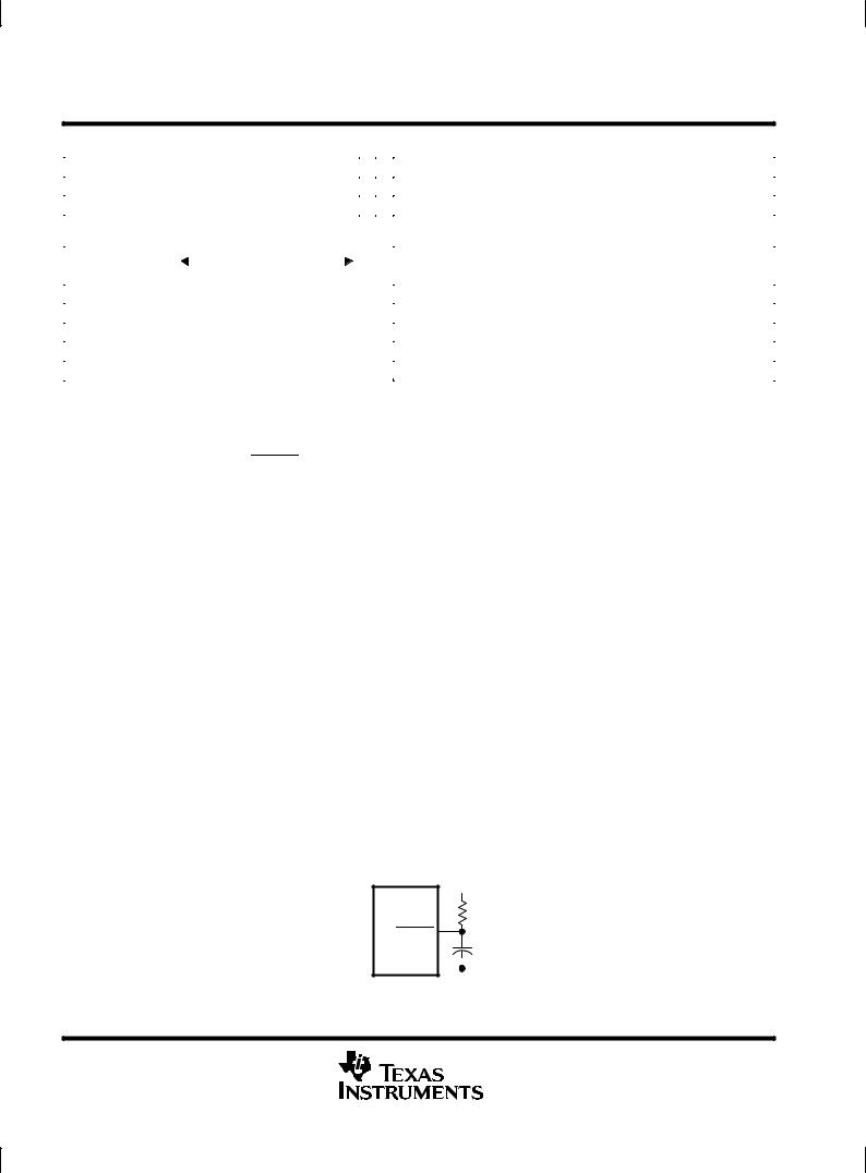
The circuit shown in Figure 1 provides a reset on power up when power is applied in the sequence given under power-up sequence. The circuit depends on the power supplies reaching their recommended values a minimum of 800 ns before the capacitor charges to 0.8 V above DGTL GND.
TLC32044/TLC32045
VCC +  5 V 200 kW
RESET
 0.5 mF
VCC ± |
|
|
± 5 V |
|
|
Figure 1. Power-Up Reset
12 |
POST OFFICE BOX 655303 •DALLAS, TEXAS 75265 |
 Loading...