


Texas Instruments TLC556CDR, TLC556CD, TLC556MN, TLC556MJB, TLC556MJ Datasheet
...TLC556, TLC556Y
DUAL LinCMOS TIMERS
SLFS047B ± FEBRUARY 1984 ± REVISED SEPTEMBER 1997
DVery Low Power Consumption . . . 2 mW Typ at VDD = 5 V
DCapable of Operation in Astable Mode
DCMOS Output Capable of Swinging Rail to Rail
DHigh Output-Current Capability
Sink 100 mA Typ
Source 10 mA Typ
DOutput Fully Compatible With CMOS, TTL, and MOS
DLow Supply Current Reduces Spikes During Output Transitions
D, J, OR N PACKAGE
(TOP VIEW)
1 DISCH |
|
1 |
14 |
|
VDD |
|
|
||||
1 THRES |
|
|
|||
|
2 |
13 |
|
2 DISCH |
|
1 CONT |
|
3 |
12 |
|
2 THRES |
|
|
||||
1 RESET |
|
4 |
11 |
|
2 CONT |
|
|
||||
1 OUT |
5 |
10 |
|
2 RESET |
|
1 TRIG |
6 |
9 |
|
2 OUT |
|
GND |
7 |
8 |
|
2 TRIG |
|
|
|
|
|
|
|
FK PACKAGE (TOP VIEW)
DSingle-Supply Operation From 2 V to 15 V
DFunctionally interchangeable With the NE556; Has Same Pinout
description
The TLC556 series are monolithic timing circuits fabricated using the TI LinCMOS process, which provides full compatibility with CMOS, TTL, and MOS logic and operates at frequencies up to 2 MHz. Accurate time delays and oscillations are possible with smaller, less-expensive timing capacitors than the NE556 because of the high input impedance. Power consumption is low across the full range of power supply voltages.
|
THRES1 |
DISCH1 |
NC |
V |
DISCH2 |
|
|
|
|
|
DD |
|
|
1 CONT |
3 |
2 |
1 |
20 19 |
2 THRES |
|
4 |
|
|
|
18 |
||
NC |
5 |
|
|
|
17 |
NC |
1 RESET |
6 |
|
|
|
16 |
2 CONT |
NC |
7 |
|
|
|
15 |
NC |
1 OUT |
8 |
|
|
|
14 |
2 RESET |
|
9 |
10 11 12 13 |
|
|||
|
1 TRIG |
GND |
NC |
2 TRIG |
2 OUT |
|
Like the NE556, the TLC556 has a trigger level approximately one-third of the supply voltage and
a threshold level approximately two-thirds of the supply voltage. These levels can be altered by use of the control voltage terminal. When the trigger input falls below the trigger level, the flip-flop is set and the output goes high. If the trigger input is above the trigger level and the threshold input is above the threshold level, the flip-flop is reset and the output is low. The reset input can override all other inputs and can be used to initiate a new timing cycle. If the reset input is low, the flip-flop is reset and the output is low. Whenever the output is low, a low-impedance path is provided between the discharge terminal and ground.
While the CMOS output is capable of sinking over 100 mA and sourcing over 10 mA, the TLC556 exhibits greatly reduced supply-current spikes during output transitions. This minimizes the need for the large decoupling capacitors required by the NE556.
These devices have internal electrostatic-discharge (ESD) protection circuits that prevent catastrophic failures at voltages up to 2000 V as tested under MIL-STD-883C, Method 3015. However, care should be exercised in handling these devices, as exposure to ESD may result in degradation of the device parametric performance.
All unused inputs should be tied to an appropriate logic level to prevent false triggering.
The TLC556C is characterized for operation from 0°C to 70°C. The TLC556I is characterized for operation from ±40°C to 85°C. The TLC556M is characterized for operation over the full military temperature range of ±55°C to 125°C.
LinCMOS is a trademark of Texas Instruments Incorporated.
PRODUCTION DATA information is current as of publication date. Products conform to specifications per the terms of Texas Instruments standard warranty. Production processing does not necessarily include testing of all parameters.
Copyright 1997, Texas Instruments Incorporated
POST OFFICE BOX 655303 •DALLAS, TEXAS 75265 |
1 |
TLC556, TLC556Y
DUAL LinCMOS TIMERS
SLFS047B ± FEBRUARY 1984 ± REVISED SEPTEMBER 1997
AVAILABLE OPTIONS
TA |
VDD |
|
|
|
PACKAGE |
|
|
|
CHIP FORM |
|||||
|
|
|
|
|
|
|
|
|
|
|||||
SMALL OUTLINE |
CHIP CARRIER |
|
CERAMIC DIP |
PLASTIC DIP |
|
|||||||||
RANGE |
RANGE |
|
|
(Y) |
||||||||||
|
(D) |
|
(FK) |
|
|
(J) |
|
(N) |
|
|||||
|
|
|
|
|
|
|
|
|
|
|
||||
|
|
|
|
|
|
|
|
|
|
|
|
|
|
|
O°C |
2 V |
|
|
|
|
|
|
|
|
|
|
|
|
|
to |
to |
|
TLC556CD |
|
|
|
|
|
TLC556CN |
|
TLC556Y |
|||
70°C |
18 V |
|
|
|
|
|
|
|
|
|
|
|
|
|
|
|
|
|
|
|
|
|
|
|
|
|
|
|
|
± 4O°C |
3 V |
|
|
|
|
|
|
|
|
|
|
|
|
|
to |
to |
|
TLC556lD |
|
|
|
|
|
TLC556IN |
|
|
|
||
85°C |
18 V |
|
|
|
|
|
|
|
|
|
|
|
|
|
|
|
|
|
|
|
|
|
|
|
|
|
|
|
|
± 55°C |
5 V |
|
|
|
|
|
|
|
|
|
|
|
|
|
to |
to |
|
TLC556MD |
|
TLC556MFK |
|
TLC556MJ |
TLC556MN |
|
|
|
|||
125°C |
18 V |
|
|
|
|
|
|
|
|
|
|
|
|
|
|
|
|
|
|
|
|
|
|
|
|
|
|
|
|
The D package is available taped and reeled. Add the suffix R to the device type (e.g., TLC556CDR). |
|
|
||||||||||||
|
|
|
|
|
|
FUNCTION TABLE |
|
|
|
|
|
|||
|
|
|
|
|
|
|
|
|
|
|
|
|||
|
|
RESET |
|
TRIGGER |
|
THRESHOLD |
|
OUTPUT |
|
DISCHARGE |
|
|||
|
|
VOLTAGE² |
|
VOLTAGE² |
|
VOLTAGE² |
|
|
SWITCH |
|
|
|||
|
|
|
|
|
|
|
|
|
||||||
|
|
< MIN |
|
Irrelevant |
|
Irrelevant |
|
L |
|
On |
|
|
||
|
|
|
|
|
|
|
|
|
|
|
|
|
||
|
|
> MAX |
|
< MIN |
|
Irrelevant |
|
H |
|
Off |
|
|
||
|
|
|
|
|
|
|
|
|
|
|
|
|
||
|
|
>MAX |
|
>MAX |
|
>MAX |
|
L |
|
On |
|
|
||
|
|
|
|
|
|
|
|
|
|
|
|
|||
|
|
> MAX |
|
> MAX |
|
< MIN |
|
As previously established |
|
|
||||
² For conditions shown as MIN or MAX, use the appropriate value specified under electrical characteristics.
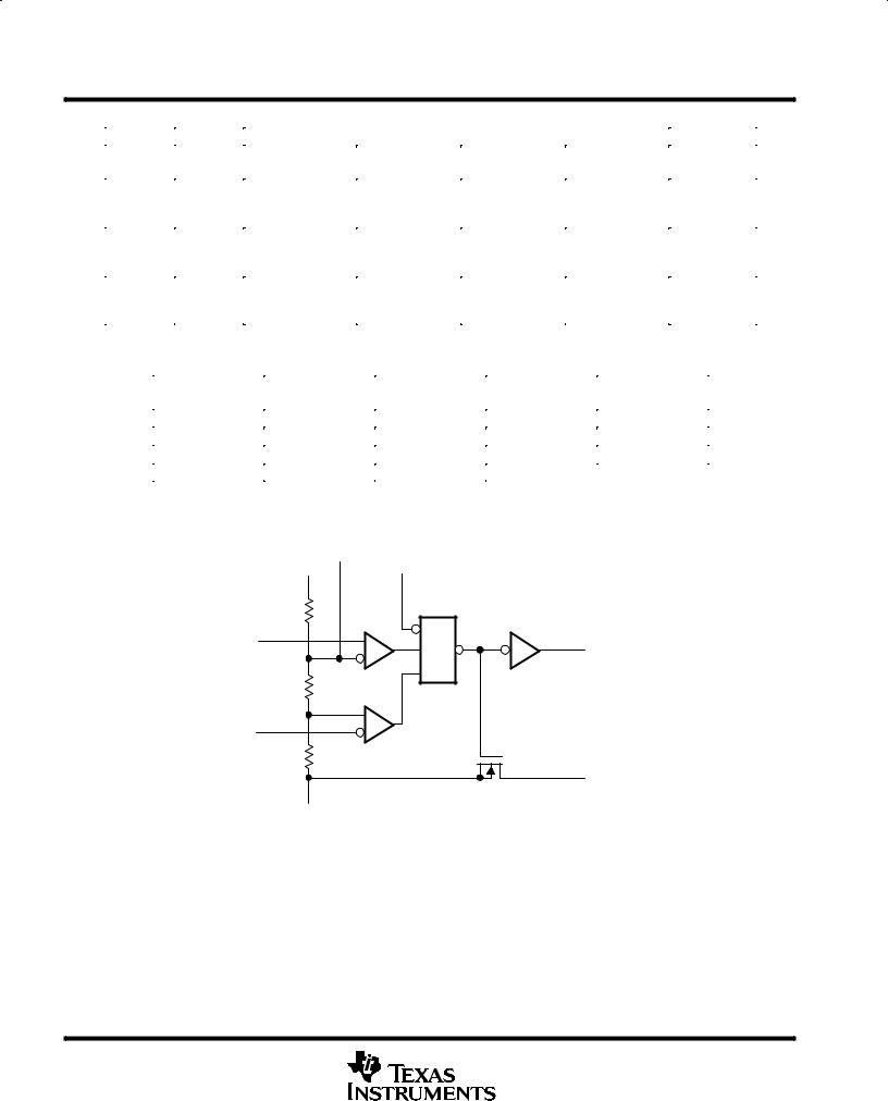
functional block diagram (each timer)
VDD |
CONT |
RESET |
|
3 |
|
||
4 |
|
||
14 |
|
|
|
R |
|
|
|
2 |
|
R1 |
5 |
THRES |
|
R 1 |
|
|
|
OUT |
|
|
|
S |
|
|
R |
|
|
6
TRIG
R
1
DISCH
7
GND
RESET can override TRIG and THRES.
TRIG can override THRES.
Pin numbers shown are for the D, J, or N packages.
2 |
POST OFFICE BOX 655303 •DALLAS, TEXAS 75265 |

TLC556, TLC556Y
DUAL LinCMOS TIMERS
SLFS047B ± FEBRUARY 1984 ± REVISED SEPTEMBER 1997
TLC556Y chip information
These chips, properly assembled, display characteristics similar to the TLC556 (see electrical table). Thermal compression or ultrasonic bonding may be used on the doped aluminum bonding pads. Chips may be mounted with conductive epoxy or a gold-silicon preform.
BONDING PAD ASSIGNMENTS
|
|
|
|
|
|
CHIP THICKNESS: 15 TYPICAL |
|
|
|
|
|
|
BONDING PADS: 4 × 4 MINIMUM |
|
|
|
|
|
|
TJ max = 150°C |
61 |
|
|
TOLERANCES ARE ± 10% |
|||
|
|
|
|
|
|
ALL DIMENSIONS ARE IN MILS |
|
|
|
|
|
||
|
|
|
|
|
|
NO BACKSIDE METALLIZATION |
|
|
|
|
|
|
PIN (7) INTERNALLY CONNECTED |
|
|
|
|
|
|
TO BACKSIDE OF CHIP |
|
|
|
|
|
|
|
|
97 |
|
|
FUNCTIONAL BLOCK DIAGRAM (EACH TIMER) |
|
||
VDD |
CONT |
RESET |
|
(3) |
|
||
(4) |
|
||
(14) |
|
|
|
|
R |
|
|
(2) |
|
R1 |
(5) |
THRESH |
|
R 1 |
|
|
|
OUT |
|
|
|
S |
|
|
R |
|
|
(6)
TRIG R
(1)
DISCH
(7) GND
POST OFFICE BOX 655303 •DALLAS, TEXAS 75265 |
3 |
TLC556, TLC556Y
DUAL LinCMOS TIMERS
SLFS047B ± FEBRUARY 1984 ± REVISED SEPTEMBER 1997
absolute maximum ratings over operating free-air temperature (unless otherwise noted)
|
|
|
|
|
|
|
TLC556C |
|
TLC556I |
|
TLC556M |
|
UNIT |
|
|
|
|
|
|
|
|
|
|
|
|
|
|
Supply voltage, VDD (see Note 1) |
|
|
|
|
18 |
|
18 |
|
18 |
|
V |
||
Input voltage range, VI |
|
|
|
|
|
± 0.3 to VDD |
|
± 0.3 to VDD |
|
± 0.3 to VDD |
|
V |
|
Sink current, discharge or output |
|
|
|
|
150 |
|
150 |
|
150 |
|
mA |
||
|
|
|
|
|
|
|
|
|
|
|
|
|
|
Source current, output |
|
|
|
|
|
15 |
|
15 |
|
15 |
|
mA |
|
|
|
|
|
|
|
|
|
|
|
|
|||
Continuous total power dissipation |
|
|
|
|
See Dissipation Rating Table |
|
|||||||
|
|
|
|
|
|
|
|
|
|
|
|
||
Operating free-air temperature range |
|
|
|
|
0 to 70 |
|
± 40 to 85 |
|
± 55 to 125 |
|
°C |
||
|
|
|
|
|
|
|
|
|
|
|
|
|
|
Storage temperature range |
|
|
|
|
± 65 to 150 |
|
± 65 to 150 |
|
± 65 to 150 |
|
°C |
||
|
|
|
|
|
|
|
|
|
|
|
|
||
Case temperature for 60 seconds |
|
FK package |
|
|
|
|
|
260 |
|
|
|||
|
|
|
|
|
|
|
|
|
|
°C |
|||
Lead temperature 1,6 mm (1/16 inch) from case for 60 seconds |
J package |
|
|
|
|
|
300 |
|
|||||
|
|
|
|
|
|
|
|
|
|
|
|||
Lead temperature 1,6 mm (1/16 inch) from case for 10 seconds |
D or N package |
|
260 |
|
260 |
|
|
|
|
||||
NOTE 1: All voltage values are with respect to network ground terminal. |
|
|
|
|
|
|
|
||||||
|
|
|
DISSIPATION RATING TABLE |
|
|
|
|
|
|
|
|||
|
|
|
|
|
|
|
|
|
|||||
|
PACKAGE |
TA ≤ 25°C |
DERATING FACTOR |
TA = 70°C |
TA = 85°C |
|
TA = 125°C |
|
|||||
|
POWER RATING |
ABOVE TA = 25°C |
|
POWER RATING POWER RATING |
POWER RATING |
|
|||||||
|
|
|
|
||||||||||
|
D |
950 mW |
7.6 mW/°C |
|
608 mW |
|
494 mW |
|
N/A |
|
|||
|
FK |
1375 mW |
11.0 mW/°C |
|
880 mW |
|
715 mW |
|
275 mW |
|
|||
|
J |
1375 mW |
11.0 mW/°C |
|
880 mW |
|
715 mW |
|
275 mW |
|
|||
|
N |
1150 mW |
9.2 mW/°C |
|
736 mW |
|
598 mW |
|
N/A |
|
|||
recommended operating conditions
|
|
MIN |
MAX |
UNIT |
|
|
|
|
|
Supply voltage, VDD |
|
2 |
15 |
V |
|
TLC556C |
0 |
70 |
|
|
|
|
|
°C |
Operating free-air temperature range, TA |
TLC556I |
± 40 |
85 |
|
|
TLC556M |
± 55 |
125 |
|
4 |
POST OFFICE BOX 655303 •DALLAS, TEXAS 75265 |
TLC556, TLC556Y
DUAL LinCMOS TIMERS
SLFS047B ± FEBRUARY 1984 ± REVISED SEPTEMBER 1997
electrical characteristics at specified free-air temperature, VDD = 2 V for TLC556C, VDD = 3 V for TLC556I
|
PARAMETER |
TEST |
T ² |
|
TLC556C |
|
|
TLC556I |
|
UNIT |
|
|
|
|
|
|
|
|
|||
|
|
CONDITIONS |
A |
MIN |
TYP |
MAX |
MIN |
TYP |
MAX |
|
|
|
|
|
|||||||
VIT |
Input threshold voltage |
|
25°C |
0.95 |
1.33 |
1.65 |
1.6 |
2 |
2.4 |
V |
|
|
|
|
|
|
|
|
|||
|
Full range |
0.85 |
|
1.75 |
1.5 |
|
2.5 |
|||
|
|
|
|
|
|
|||||
|
|
|
|
|
|
|
|
|
|
|
|
Threshold current |
|
25°C |
|
10 |
|
|
10 |
|
pA |
|
|
|
|
|
|
|
|
|
||
|
|
MAX |
|
75 |
|
|
150 |
|
||
|
|
|
|
|
|
|
|
|||
|
|
|
|
|
|
|
|
|
|
|
V(trigger) |
Trigger voltage |
|
25°C |
0.4 |
0.67 |
0.95 |
0.71 |
1 |
1.29 |
V |
|
|
|
|
|
|
|
|
|||
|
Full range |
0.3 |
|
1.05 |
0.61 |
|
1.39 |
|||
|
|
|
|
|
|
|||||
|
|
|
|
|
|
|
|
|
|
|
I(trigger) |
Trigger current |
|
25°C |
|
10 |
|
|
10 |
|
pA |
|
|
|
|
|
|
|
|
|||
|
MAX |
|
75 |
|
|
150 |
|
|||
|
|
|
|
|
|
|
|
|||
|
|
|
|
|
|
|
|
|
|
|
V(reset) |
Reset voltage |
|
25°C |
0.4 |
1.1 |
1.5 |
0.4 |
1.1 |
1.5 |
V |
|
|
|
|
|
|
|
|
|||
|
Full range |
0.3 |
|
1.8 |
0.3 |
|
1.8 |
|||
|
|
|
|
|
|
|||||
|
|
|
|
|
|
|
|
|
|
|
I(reset) |
Reset current |
|
25°C |
|
10 |
|
|
10 |
|
pA |
|
|
|
|
|
|
|
|
|||
|
MAX |
|
75 |
|
|
150 |
|
|||
|
|
|
|
|
|
|
|
|||
|
|
|
|
|
|
|
|
|
|
|
|
Control voltage (open circuit) as |
|
MAX |
|
66.7% |
|
|
66.7% |
|
|
|
a percentage of supply voltage |
|
|
|
|
|
|
|||
|
|
|
|
|
|
|
|
|
|
|
|
|
|
|
|
|
|
|
|
|
|
|
Discharge switch on-state volt- |
IOL = 1 mA |
25°C |
|
0.04 |
0.2 |
|
0.03 |
0.2 |
V |
|
age |
Full range |
|
|
0.25 |
|
|
0.375 |
||
|
|
|
|
|
|
|
||||
|
|
|
|
|
|
|
|
|
|
|
|
Discharge switch off-state cur- |
|
25°C |
|
0.1 |
|
|
0.1 |
|
nA |
|
rent |
|
MAX |
|
0.5 |
|
|
120 |
|
|
|
|
|
|
|
|
|
||||
|
|
|
|
|
|
|
|
|
|
|
VOH |
High-level output voltage |
IOH = ±300 A |
25°C |
1.5 |
1.9 |
|
1.5 |
1.9 |
|
V |
|
|
|
|
|
|
|
||||
Full range |
1.5 |
|
|
2.5 |
|
|
||||
|
|
|
|
|
|
|
|
|||
|
|
|
|
|
|
|
|
|
|
|
VOL |
Low-level output voltage |
IOL = 1 mA |
25°C |
|
0.07 |
0.3 |
|
0.07 |
0.3 |
V |
|
|
|
|
|
|
|
||||
Full range |
|
|
0.35 |
|
|
0.4 |
||||
|
|
|
|
|
|
|
|
|||
|
|
|
|
|
|
|
|
|
|
|
IDD |
Supply current |
See Note 2 |
25°C |
|
130 |
500 |
|
130 |
500 |
A |
|
|
|
|
|
|
|
||||
Full range |
|
|
800 |
|
|
1000 |
||||
|
|
|
|
|
|
|
|
|||
|
|
|
|
|
|
|
|
|
|
|
² Full range is 0°C to 70°C for TLC556C and ± 40°C to 85°C for TLC556I.
NOTE 2: These values apply for the expected operating configurations in which THRES is connected directly to DISCH or TRIG.
POST OFFICE BOX 655303 •DALLAS, TEXAS 75265 |
5 |
 Loading...