


TLC2272QD
Texas Instruments TLC2272QD, TLC2272QDR, TLC2272MUB, TLC2272MP, TLC2272MJGB Datasheet
...
TLC227x, TLC227xA
Advanced LinCMOS RAIL-TO-RAIL
OPERATIONAL AMPLIFIERS
SLOS190B – FEBRUARY 1997 – REVISED JULY 1999
1
POST OFFICE BOX 655303 • DALLAS, TEXAS 75265
D
Output Swing Includes Both Supply Rails
D
Low Noise ...9 nV/√Hz Typ at f = 1 kHz
D
Low Input Bias Current ...1 pA Typ
D
Fully Specified for Both Single-Supply and
Split-Supply Operation
D
Common-Mode Input Voltage Range
Includes Negative Rail
D
High-Gain Bandwidth . . . 2.2 MHz Typ
D
High Slew Rate . . . 3.6 V/µs Typ
D
Low Input Offset Voltage
950 µV Max at T
A
= 25°C
D
Macromodel Included
D
Performance Upgrades for the TS272,
TS274, TLC272, and TLC274
D
Available in Q-Temp Automotive
HighRel Automotive Applications
Configuration Control / Print Support
Qualification to Automotive Standards
description
The TLC2272 and TLC2274 are dual and
quadruple operational amplifiers from Texas
Instruments. Both devices exhibit rail-to-rail
output performance for increased dynamic range
in single- or split-supply applications. The
TLC227x family offers 2 MHz of bandwidth and
3 V/µs of slew rate for higher speed applications.
These devices offer comparable ac performance
while having better noise, input offset voltage, and
power dissipation than existing CMOS
operational amplifiers. The TLC227x has a noise
voltage of 9 nV/√Hz
, two times lower than
competitive solutions.
The TLC227x, exhibiting high input impedance
and low noise, is excellent for small-signal
conditioning for high-impedance sources, such as
piezoelectric transducers. Because of the micro-
power dissipation levels, these devices work well
in hand-held monitoring and remote-sensing
applications. In addition, the rail-to-rail output
feature, with single- or split-supplies, makes this
family a great choice when interfacing with
analog-to-digital converters (ADCs). For precision applications, the TLC227xA family is available and has a
maximum input offset voltage of 950 µV. This family is fully characterized at 5 V and ±5 V.
The TLC2272/4 also makes great upgrades to the TLC272/4 or TS272/4 in standard designs. They offer
increased output dynamic range, lower noise voltage, and lower input offset voltage. This enhanced feature set
allows them to be used in a wider range of applications. For applications that require higher output drive and
wider input voltage range, see the TLV2432 and TLV2442 devices.
If the design requires single amplifiers, please see the TLV2211/21/31 family. These devices are single
rail-to-rail operational amplifiers in the SOT-23 package. Their small size and low power consumption, make
them ideal for high density, battery-powered equipment.
Copyright 1999, Texas Instruments Incorporated
PRODUCTION DATA information is current as of publication date.
Products conform to specifications per the terms of Texas Instruments
standard warranty. Production processing does not necessarily include
testing of all parameters.
Please be aware that an important notice concerning availability, standard warranty, and use in critical applications of
Texas Instruments semiconductor products and disclaimers thereto appears at the end of this data sheet.
Advanced LinCMOS is a trademark of Texas Instruments Incorporated.
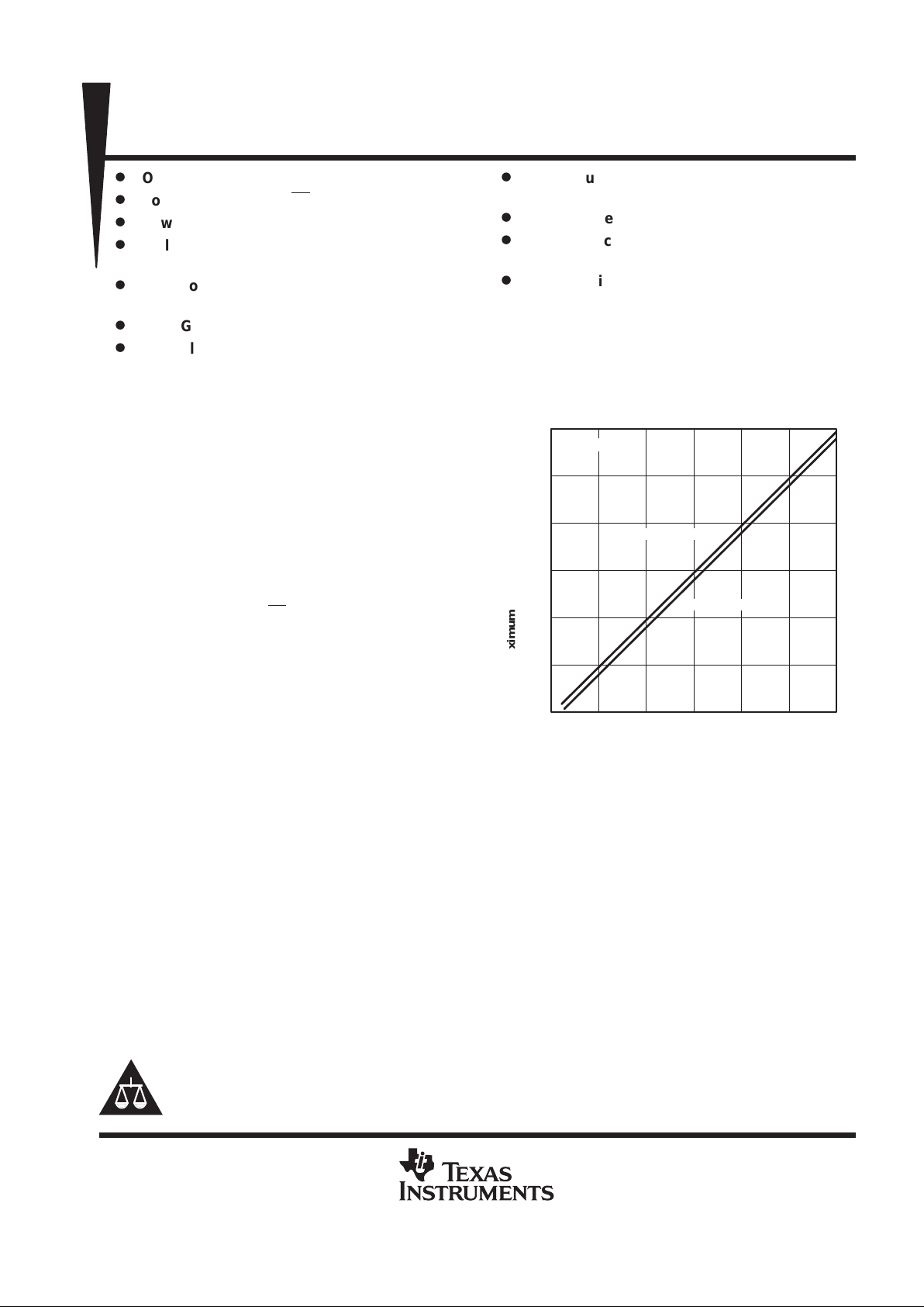
|V
DD±
| – Supply Voltage – V
10
8
6
4
46 8
12
14
16
10 12 14
16
MAXIMUM PEAK-TO-PEAK OUTPUT VOLTAGE
vs
SUPPLY VOLTAGE
T
A
= 25°C
I
O
= ±50 µA
I
O
= ±500 µA
V(OPP) – Maximum Peak-to-Peak Output Voltage – VV
O(PP)
On products compliant to MIL-PRF-38535, all parameters are tested
unless otherwise noted. On all other products, production
processing does not necessarily include testing of all parameters.
TLC227x, TLC227xA
Advanced LinCMOS RAIL-TO-RAIL
OPERATIONAL AMPLIFIERS
SLOS190B – FEBRUARY 1997 – REVISED JULY 1999
2
POST OFFICE BOX 655303 • DALLAS, TEXAS 75265
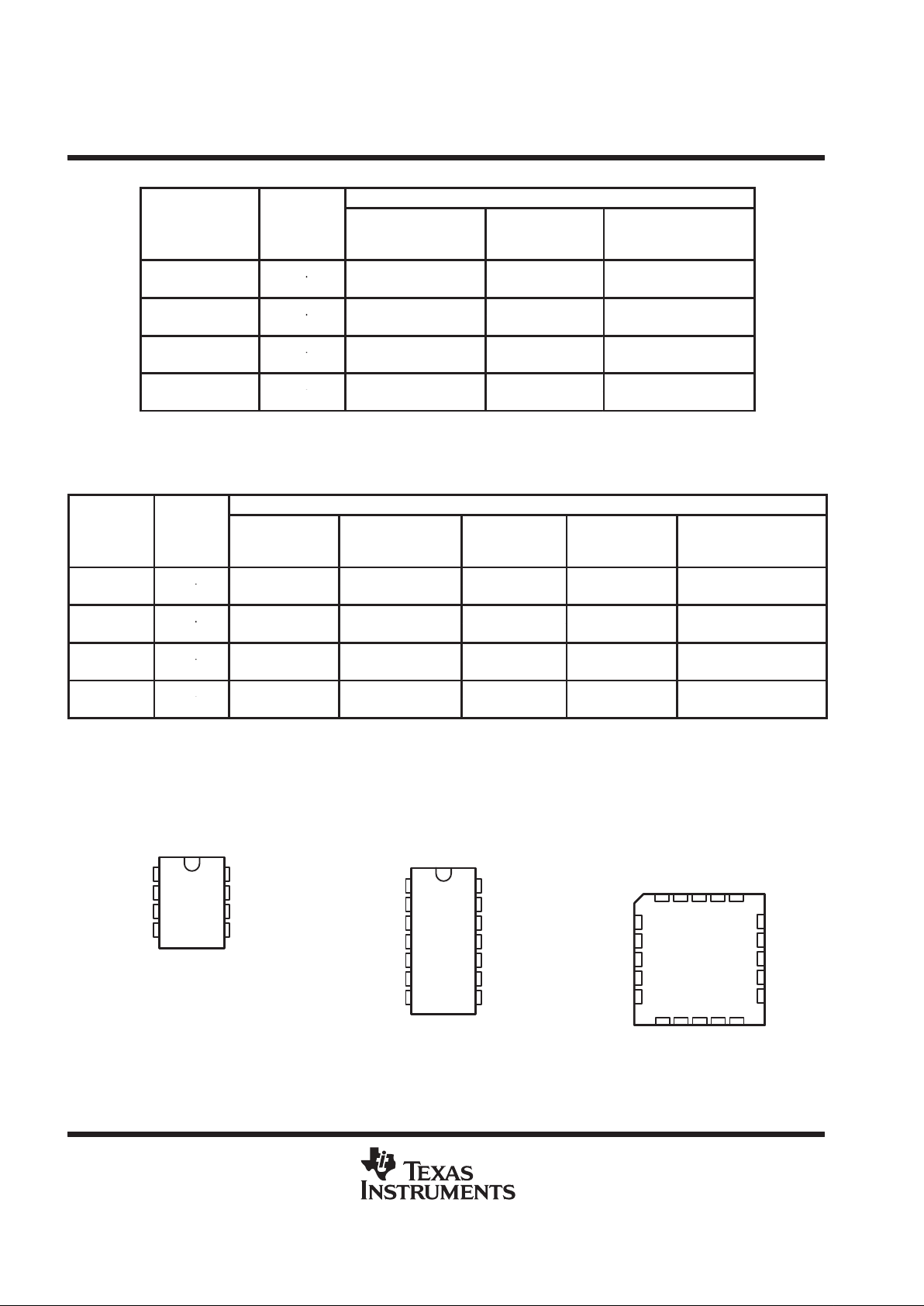
TLC2272 A VAILABLE OPTIONS
PACKAGED DEVICES
T
A
V
IO
max At
25°C
SMALL
OUTLINE
†
(D)
PLASTIC DIP
(P)
TSSOP
‡
(PW)
°
°
950 µV TLC2272ACD TLC2272ACP
0°C
to
70°C
µ
2.5 mV TLC2272CD TLC2272CP
TLC2272CPW
°
°
950
µ
V TLC2272AID TLC2272AIP
–
40°C
to
85°C
µ
2.5 mV TLC2272ID TLC2272IP
—
°
°
950
µ
V TLC2272AQD TLC2272AQPW
–
40°C
to
125°C
µ
2.5 mV TLC2272QD
—
TLC2272QPW
°
°
950 µV TLC2272AMD TLC2272AMP
–
55°C
to
125°C
µ
2.5 mV TLC2272MD TLC2272MP
—
†
The D packages are available taped and reeled. Add R suffix to the device type (e.g., TLC2272CDR).
‡
The PW package is available taped and reeled. Add R suffix to the device type (e.g., TLC2272PWR).
§
Chips are tested at 25°C.
TLC2274 AVAILABLE OPTIONS
PACKAGED DEVICES
T
A
V
IO
max AT
25°C
SMALL
OUTLINE
†
(D)
CHIP
CARRIER
(FK)
CERAMIC
DIP
(J)
PLASTIC
DIP
(N)
TSSOP
‡
(PW)
0°C to 950
µ
V TLC2274ACD TLC2274ACN —
70°C
µ
2.5 mV TLC2274CD
— —
TLC2274CN TLC2274CPW
–40°C to 950
µ
V TLC2274AID TLC2274AIN —
85°C
µ
2.5 mV TLC2274ID
— —
TLC2274IN TLC2274IPW
–40°C to 950
µ
V TLC2274AQD
125°C
µ
2.5 mV TLC2274QD
— — — —
–55°C to 950 µV TLC2274AMD TLC2274AMFK TLC2274AMJ TLC2274AMN
125°C
µ
2.5 mV TLC2274MD TLC2274MFK TLC2274MJ TLC2274MN
—
†
The D packages are available taped and reeled. Add R suffix to device type (e.g., TLC2274CDR).
‡
The PW package is available taped and reeled.
§
Chips are tested at 25°C.
1
2
3
4
8
7
6
5
1OUT
1IN–
1IN+
V
DD–
/GND
V
DD+
2OUT
2IN–
2IN+
TLC2272
D, P, OR PW PACKAGE
(TOP VIEW)
1
2
3
4
5
6
7
14
13
12
11
10
9
8
1OUT
1IN–
1IN+
V
DD+
2IN+
2IN–
2OUT
4OUT
4IN–
4IN+
V
DD–
3IN+
3IN–
3OUT
3212019
910111213
4
5
6
7
8
18
17
16
15
14
4IN+
NC
V
DD–
NC
3IN+
1IN+
NC
V
DD+
NC
2IN+
1IN –
1OUT
NC
3IN –
4IN –
2IN –
2OUT
NC
NC – No internal connection
3OUT
4OUT
TLC2274
D, J, N, OR PW PACKAGE
(TOP VIEW)
TLC2274
FK PACKAGE
(TOP VIEW)
TLC227x, TLC227xA
OPERATIONAL AMPLIFIERS
SLOS190B – FEBRUARY 1997 – REVISED JUL Y 1999
Advanced LinCMOS RAIL-TO-RAIL
POST OFFICE BOX 655303 DALLAS, TEXAS 75265
• 3
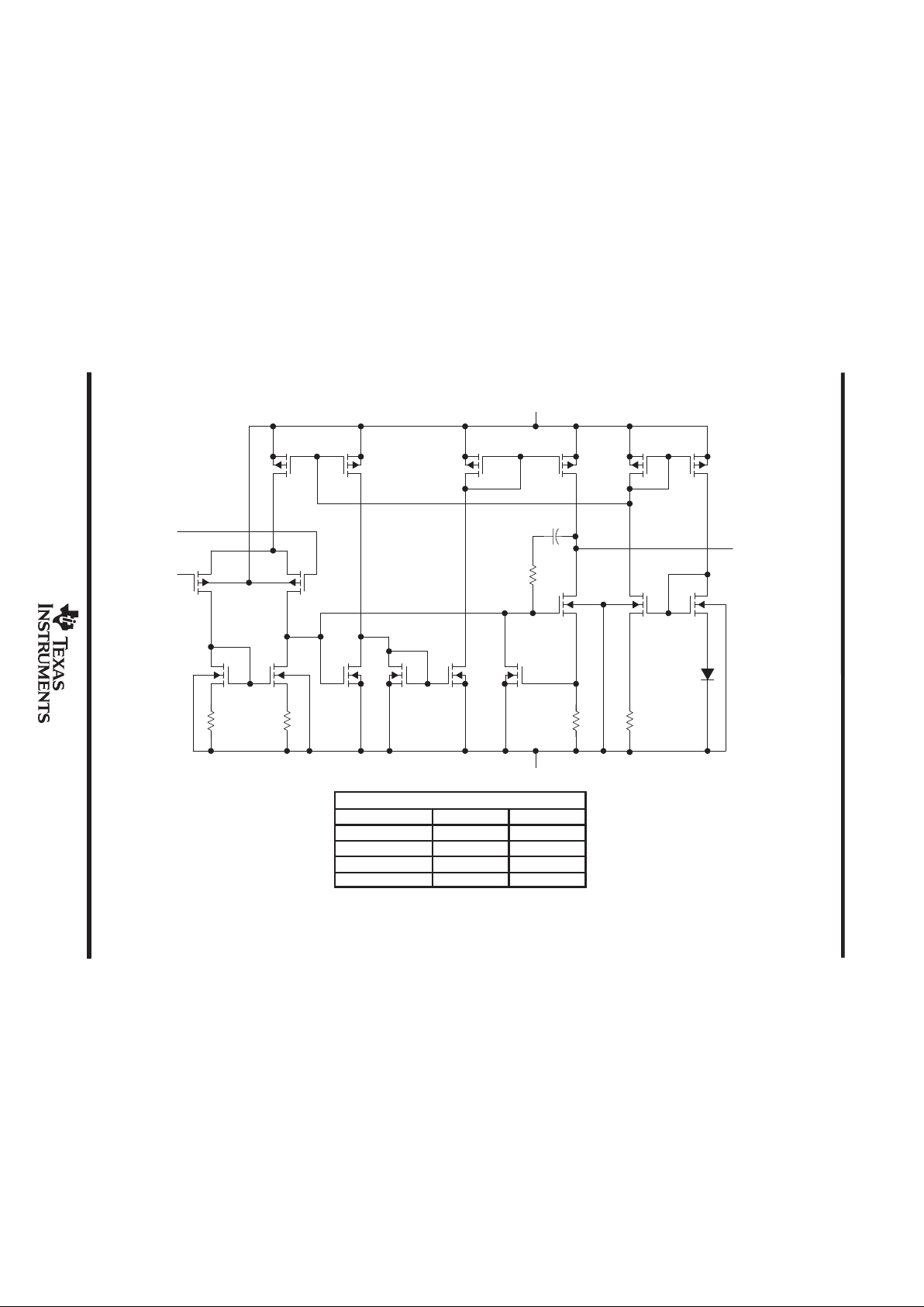
equivalent schematic (each amplifier)
Q3 Q6 Q9 Q12 Q14 Q16
Q2 Q5 Q7 Q8 Q10 Q11
D1
Q17Q15Q13
Q4Q1
R5
C1
V
DD+
IN+
IN–
R3 R4 R1 R2
OUT
V
DD
–
ACTUAL DEVICE COMPONENT COUNT
†
COMPONENT TLC2272 TLC2274
Transistors 38 76
Resistors 26 52
Diodes 9 18
Capacitors 3 6
†
Includes both amplifiers and all ESD, bias, and trim circuitry
TLC227x, TLC227xA
Advanced LinCMOS RAIL-TO-RAIL
OPERATIONAL AMPLIFIERS
SLOS190B – FEBRUARY 1997 – REVISED JULY 1999
4
POST OFFICE BOX 655303 • DALLAS, TEXAS 75265
absolute maximum ratings over operating free-air temperature range (unless otherwise noted)
†
Supply voltage, V
DD+
(see Note 1) 8 V. . . . . . . . . . . . . . . . . . . . . . . . . . . . . . . . . . . . . . . . . . . . . . . . . . . . . . . . . . . .
Supply voltage, V
DD–
(see Note 1) –8 V. . . . . . . . . . . . . . . . . . . . . . . . . . . . . . . . . . . . . . . . . . . . . . . . . . . . . . . . . . .
Differential input voltage, V
ID
(see Note 2) ±16 V. . . . . . . . . . . . . . . . . . . . . . . . . . . . . . . . . . . . . . . . . . . . . . . . . . .
Input voltage, V
I
(any input, see Note 1) V
DD–
– 0.3 V to V
DD+
. . . . . . . . . . . . . . . . . . . . . . . . . . . . . . . . . . . . . .
Input current, I
I
(any input) ±5 mA. . . . . . . . . . . . . . . . . . . . . . . . . . . . . . . . . . . . . . . . . . . . . . . . . . . . . . . . . . . . . . . .
Output current, I
O
±50 mA. . . . . . . . . . . . . . . . . . . . . . . . . . . . . . . . . . . . . . . . . . . . . . . . . . . . . . . . . . . . . . . . . . . . . . .
Total current into V
DD+
±50 mA. . . . . . . . . . . . . . . . . . . . . . . . . . . . . . . . . . . . . . . . . . . . . . . . . . . . . . . . . . . . . . . . . .
Total current out of V
DD–
±50 mA. . . . . . . . . . . . . . . . . . . . . . . . . . . . . . . . . . . . . . . . . . . . . . . . . . . . . . . . . . . . . . . .
Duration of short-circuit current at (or below) 25°C (see Note 3) unlimited. . . . . . . . . . . . . . . . . . . . . . . . . . . . . .
Continuous total dissipation See Dissipation Rating Table. . . . . . . . . . . . . . . . . . . . . . . . . . . . . . . . . . . . . . . . . . .
Operating free-air temperature range, T
A
: C suffix 0°C to 70°C. . . . . . . . . . . . . . . . . . . . . . . . . . . . . . . . . . . . . .
I suffix –40°C to 85°C. . . . . . . . . . . . . . . . . . . . . . . . . . . . . . . . . . . . .
Q suffix –40°C to 125°C. . . . . . . . . . . . . . . . . . . . . . . . . . . . . . . . . . .
M suffix –55°C to 125°C. . . . . . . . . . . . . . . . . . . . . . . . . . . . . . . . . .
Storage temperature range –65°C to 150°C. . . . . . . . . . . . . . . . . . . . . . . . . . . . . . . . . . . . . . . . . . . . . . . . . . . . . . . .
Lead temperature 1,6 mm (1/16 inch) from case for 10 seconds: D, N, P or PW package 260°C. . . . . . . . . .
Lead temperature 1,6 mm (1/16 inch) from case for 60 seconds: J package 300°C. . . . . . . . . . . . . . . . . . . . .
†
Stresses beyond those listed under “absolute maximum ratings” may cause permanent damage to the device. These are stress ratings only, and
functional operation of the device at these or any other conditions beyond those indicated under “recommended operating conditions” is not
implied. Exposure to absolute-maximum-rated conditions for extended periods may affect device reliability.
NOTES: 1. All voltage values, except differential voltages, are with respect to the midpoint between V
DD+
and V
DD –
.
2. Differential voltages are at IN+ with respect to IN–. Excessive current will flow if input is brought below V
DD–
– 0.3 V.
3. The output may be shorted to either supply. Temperature and/or supply voltages must be limited to ensure that the maximum
dissipation rating is not exceeded.
DISSIPATION RATING TABLE
T
≤ 25°C DERATING FACTOR T
= 70°C T
= 85°C T
= 125°C
PACKAGE
A
POWER RATING ABOVE T
A
= 25°C
A
POWER RATING
A
POWER RATING
A
POWER RATING
D–8 725 mW 5.8 mW/°C 464 mW 337 mW 145 mW
D–14 950 mW 7.6 mW/°C 608 mW 494 mW 190 mW
FK 1375 mW 11.0 mW/°C 880 mW 715 mW 275 mW
J 1375 mW 11.0 mW/°C 880 mW 715 mW 275 mW
N 1150 mW 9.2 mW/°C 736 mW 598 mW 230 mW
P 1000 mW 8.0 mW/°C 640 mW 520 mW 200 mW
PW–8 525 mW 4.2 mW/°C 336 mW 273 mW 105 mW
PW–14 700 mW 5.6 mW/°C 448 mW 364 mW —
recommended operating conditions
C SUFFIX I SUFFIX Q SUFFIX M SUFFIX
MIN MAX MIN MAX MIN MAX MIN MAX
UNIT
Supply voltage, V
DD±
±2.2 ±8 ±2.2 ±8 ±2.2 ±8 ±2.2 ±8 V
Input voltage range, V
I
V
DD–
V
DD+
–1.5 V
DD–
V
DD+
–1.5 V
DD–
V
DD+
–1.5 V
DD–
V
DD+
–1.5 V
Common-mode input voltage, V
IC
V
DD–
V
DD+
–1.5 V
DD–
V
DD+
–1.5 V
DD–
V
DD+
–1.5 V
DD–
V
DD+
–1.5 V
Operating free-air temperature, T
A
0 70 –40 85 –40 125 –55 125 °C
TLC227x, TLC227xA
Advanced LinCMOS RAIL-TO-RAIL
OPERATIONAL AMPLIFIERS
SLOS190B – FEBRUARY 1997 – REVISED JULY 1999
5
POST OFFICE BOX 655303 • DALLAS, TEXAS 75265
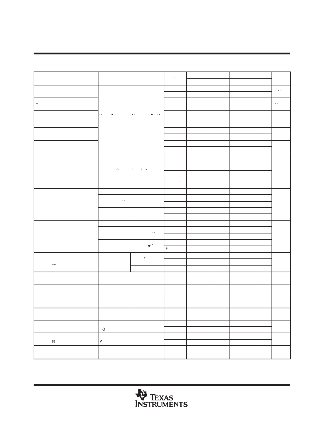
TLC2272C electrical characteristics at specified free-air temperature, V
DD
= 5 V (unless otherwise
noted)
TLC2272C TLC2272AC
PARAMETER
TEST
CONDITIONS
T
A
†
MIN TYP MAX MIN TYP MAX
UNIT
p
25°C 300 2500 300 950
V
IO
Inp
u
t
offset
v
oltage
Full range 3000 1500
µ
V
T emperature coef ficient
25°C
°
α
VIO
of input offset voltage
to 70°C
2
2
µ
V/°C
Input offset voltage
long-term drift
(see Note 4)
V
IC
= 0,
V
O
= 0,
V
DD
± = ±2.5
V
,
R
S
= 50 Ω
25°C
0.002 0.002 µV/mo
p
25°C 0.5 0.5
p
I
IO
Inp
u
t
offset
c
u
rrent
Full range 100 100
pA
p
25°C 1 1
p
I
IB
Inp
u
t
bias
c
u
rrent
Full range 100 100
pA
°
0
–0.3
0
–0.3
Common-mode input
25°C
to
4
to
4.2
to
4
to
4.2
V
ICR
voltage range
R
S
=
50
Ω
,
|V
IO
|
≤ 5
mV
0 0
V
Full range
to to
g
3.5 3.5
I
OH
= –20 µA 25°C 4.99 4.99
25°C 4.85 4.93 4.85 4.93
V
OH
Hi
g
h
-
l
eve
l
ou
t
pu
t
I
OH
= –
200
µ
A
Full range 4.85 4.85
V
voltage
25°C 4.25 4.65 4.25 4.65
I
OH
= –
1
mA
Full range 4.25 4.25
V
IC
= 2.5 V, I
OL
= 50 µA 25°C 0.01 0.01
25°C 0.09 0.15 0.09 0.15
V
OL
L
ow-
l
eve
l
ou
t
pu
t
V
IC
=
2
.
5
V
,
I
OL
=
500
µ
A
Full range 0.15 0.15
V
voltage
25°C 0.9 1.5 0.9 1.5
V
IC
=
2
.
5
V
,
I
OL
=
5
m
A
Full range 1.5 1.5
25°C 15 35 15 35
A
VD
L
arge-s
i
gna
l
diff
eren
ti
a
l
p
V
IC
=
2
.
5
V
,
R
L
=
10
kΩ
‡
Full range 15 15
V/mV
VD
voltage
am lification
V
O
=
1
V
to
4
V
R
L
= 1 mΩ
‡
25°C 175 175
r
id
Differential input
resistance
25°C 10
12
10
12
Ω
r
i
Common-mode input
resistance
25°C 10
12
10
12
Ω
c
i
Common-mode input
capacitance
f = 10 kHz, P package 25°C 8 8 pF
z
o
Closed-loop output
impedance
f = 1 MHz, A
V
= 10 25°C 140 140
Ω
Common-mode
V
= 0 to 2.7 V,
25°C 70 75 70 75
CMRR
rejection ratio
IC
,
V
O
= 2.5 V, R
S
= 50 Ω
Full range 70 70
dB
Supply-voltage rejection V
DD
= 4.4 V to 16 V,
25°C 80 95 80 95
k
SVR
ygj
ratio (∆V
DD
/∆V
IO
)
DD
V
IC
= V
DD
/2, No load
Full range 80 80
dB
pp
25°C 2.2 3 2.2 3
I
DD
S
u
ppl
y
c
u
rrent
V
O
=
2
.
5
V
,
No
load
Full range 3 3
mA
†
Full range is 0°C to 70°C.
‡
Referenced to 2.5 V
NOTE 4: T ypical values are based on the input offset voltage shift observed through 168 hours of operating life test at T
A
= 150°C extrapolated
to T
A
= 25°C using the Arrhenius equation and assuming an activation energy of 0.96 eV .
TLC227x, TLC227xA
Advanced LinCMOS RAIL-TO-RAIL
OPERATIONAL AMPLIFIERS
SLOS190B – FEBRUARY 1997 – REVISED JULY 1999
6
POST OFFICE BOX 655303 • DALLAS, TEXAS 75265
TLC2272C operating characteristics at specified free-air temperature, V
DD
= 5 V
TLC2272C TLC2272AC
PARAMETER
TEST
CONDITIONS
T
A
†
MIN TYP MAX MIN TYP MAX
UNIT
V
O
= 0.5 V to 2.5 V,
25°C 2.3 3.6 2.3 3.6
SR
Slew
rate
at
unity
g
ain
R
L
= 10 kΩ
‡
, C
L
= 100 pF
‡
Full
V/µs
g
range
1
.
7
1
.
7
Equivalent input
f = 10 Hz 25°C 50 50
V
n
q
noise voltage
f = 1 kHz
25°C 9 9
n
V/√H
z
Peak-to-peak
p
f = 0.1 Hz to 1 Hz 25°C 1 1
V
NPP
equ
i
va
l
en
t
i
npu
t
noise voltage
f = 0.1 Hz to 10 Hz
25°C 1.4 1.4
µ
V
I
n
Equivalent input
noise current
25°C 0.6 0.6
fA/√Hz
=
A
V
= 1 0.0013% 0.0013%
THD + N
Total harmonic
p
V
O
=
0
.
5
V
to
2
.
5
V
,
f = 20 kHz,
A
V
= 10
25°C
0.004% 0.004%
distortion
lus
noise
R
L
= 10 kΩ
‡
,
A
V
= 100 0.03% 0.03%
Gain-bandwidth
product
f = 10 kHz,
C
L
= 100 pF
‡
R
L
= 10 kΩ
‡
,
25°C 2.18 2.18 MHz
B
OM
Maximum
output-swing
bandwidth
V
O(PP)
= 2 V,
R
L
= 10 kΩ
‡
,
A
V
= 1,
C
L
= 100 pF
‡
25°C 1 1 MHz
=–
A
V
=
1
,
Step = 0.5 V to 2.5 V ,
To
0
.
1%
°
1
.
5
1
.
5
t
s
Settling
time
,
R
L
= 10 kΩ
‡
,
25°C
µ
s
L
C
L
= 100 pF
‡
To
0
.
01%
2
.
6
2
.
6
φ
m
Phase margin at
unity gain
R
= 10 kΩ
‡
, C
= 100 pF
‡
25°C
50° 50°
Gain margin
L
,
L
25°C 10 10 dB
†
Full range is 0°C to 70°C.
‡
Referenced to 2.5 V
TLC227x, TLC227xA
Advanced LinCMOS RAIL-TO-RAIL
OPERATIONAL AMPLIFIERS
SLOS190B – FEBRUARY 1997 – REVISED JULY 1999
7
POST OFFICE BOX 655303 • DALLAS, TEXAS 75265
TLC2272C electrical characteristics at specified free-air temperature, V
DD±
= ±5 V (unless
otherwise specified)
TLC2272C TLC2272AC
PARAMETER
TEST
CONDITIONS
T
A
†
MIN TYP MAX MIN TYP MAX
UNIT
p
25°C 300 2500 300 950
V
IO
Inp
u
t
offset
v
oltage
Full range 3000 1500
µ
V
T emperature coef ficient of
25°C
°
α
VIO
input offset voltage
to 70°C
2
2
µ
V/°C
Input offset voltage
long-term drift
(see Note 4)
V
IC
= 0,
R
S
= 50 Ω
V
O
= 0,
25°C
0.002 0.002 µV/mo
p
25°C 0.5 0.5
p
I
IO
Inp
u
t
offset
c
u
rrent
Full range 100 100
pA
p
25°C 1 1
p
I
IB
Inp
u
t
bias
c
u
rrent
Full range 100 100
pA
–5 –5.3 –5 –5.3
25°C
to to to to
Common-mode input
4 4.2 4 4.2
V
ICR
voltage range
R
S
=
50
Ω
,
|V
IO
|
≤5
mV
–5 –5
V
Full range
to to
g
3.5 3.5
I
O
= –20 µA 25°C 4.99 4.99
25°C 4.85 4.93 4.85 4.93
V
OM+
M
ax
i
mum pos
iti
ve pea
k
p
I
O
= –
200
µ
A
Full range 4.85 4.85
V
out ut
voltage
25°C 4.25 4.65 4.25 4.65
I
O
= –
1
mA
Full range 4.25 4.25
V
IC
= 0, I
O
= 50 µA 25°C –4.99 –4.99
25°C –4.85 –4.91 –4.85 –4.91
V
OM–
M
ax
i
mum nega
ti
ve pea
k
p
V
IC
=
0
,
I
O
=
500
µ
A
Full range –4.85 –4.85
V
out ut
voltage
25°C –3.5 –4.1 –3.5 –4.1
V
IC
=
0
,
I
O
=
5
m
A
Full range –3.5 –3.5
25°C 25 50 25 50
A
VD
L
arge-s
i
gna
l
diff
eren
ti
a
l
p
V
O
= ±4 V
R
L
=
10
kΩ
Full range 25 25
V/mV
voltage
am lification
R
L
= 1 mΩ 25°C 300 300
r
id
Differential input
resistance
25°C 10
12
10
12
Ω
r
i
Common-mode input
resistance
25°C 10
12
10
12
Ω
c
i
Common-mode input
capacitance
f = 10 kHz, P package 25°C 8 8 pF
z
o
Closed-loop output
impedance
f = 1 MHz, A
V
= 10 25°C 130 130
Ω
Common-mode rejection
V
= –5 to 2.7 V,
25°C 75 80 75 80
CMRR
j
ratio
IC
,
V
O
= 0 V, R
S
= 50 Ω
Full range 75 75
dB
Supply-voltage rejection
V
DD±
= 2.2
V
to ±8
V
,
25°C 80 95 80 95
k
SVR
ygj
ratio (∆V
DD±
/∆V
IO
)
DD±
V
IC
= 0, No load
Full range 80 80
dB
pp
25°C 2.4 3 2.4 3
I
DD
S
u
ppl
y
c
u
rrent
V
O
=
0
V
No
load
Full range 3 3
mA
†
Full range is 0°C to 70°C.
NOTE 4: T ypical values are based on the input offset voltage shift observed through 168 hours of operating life test at T
A
= 150°C extrapolated
to T
A
= 25°C using the Arrhenius equation and assuming an activation energy of 0.96 eV .
TLC227x, TLC227xA
Advanced LinCMOS RAIL-TO-RAIL
OPERATIONAL AMPLIFIERS
SLOS190B – FEBRUARY 1997 – REVISED JULY 1999
8
POST OFFICE BOX 655303 • DALLAS, TEXAS 75265
TLC2272C operating characteristics at specified free-air temperature, V
DD±
= ±5 V
TLC2272C TLC2272AC
PARAMETER
TEST
CONDITIONS
T
A
†
MIN TYP MAX MIN TYP MAX
UNIT
25°C 2.3 3.6 2.3 3.6
SR
Sle
w
rate
at
V
O
=
±2
.
3
V
,
=
p
R
L
=
10
kΩ
,
Full
V/µs
unity
gain
C
L
=
100
F
range
1
.
7
1
.
7
Equivalent input
f = 10 Hz 25°C 50 50
V
n
q
noise voltage
f = 1 kHz
25°C 9 9
n
V/√H
z
Peak-to-peak
p
f = 0.1 Hz to 1 Hz 25°C 1 1
V
NPP
equ
i
va
l
en
t
i
npu
t
noise voltage
f = 0.1 Hz to 10 Hz
25°C 1.4 1.4
µ
V
I
n
Equivalent input
noise current
25°C 0.6 0.6
fA/√Hz
=
A
V
= 1 0.0011% 0.0011%
THD + N
Total
harmonic
distortion pulse
V
O
=
±2
.
3
V
,
f = 20 kHz,
A
V
= 10
25°C
0.004% 0.004%
duration R
L
= 10 kΩ
A
V
= 100 0.03% 0.03%
Gain-bandwidth f = 10 kHz, R
= 10 kΩ,
°
product
,
C
L
= 100 pF
L
,
25°C
2
.
25
2
.
25
MH
z
Maximum output- V
= 4.6 V, A
= 1,
°
B
OM
swing bandwidth
O(PP)
,
R
L
= 10 kΩ,
V
,
C
L
= 100 pF
25°C
0
.
54
0
.
54
MH
z
=–
A
V
=
1
,
Step = –2.3 V to 2.3 V,
To
0
.
1%
°
1
.
5
1
.
5
t
s
Settling
time
,
R
L
= 10 kΩ,
25°C
µ
s
L
C
L
= 100 pF
To
0
.
01%
3
.
2
3
.
2
φ
m
Phase margin at
unity gain
R
L
= 10 kΩ, C
L
= 100 pF
25°C
52° 52°
Gain margin
L
L
25°C 10 10 dB
†
Full range is 0°C to 70°C.
TLC227x, TLC227xA
Advanced LinCMOS RAIL-TO-RAIL
OPERATIONAL AMPLIFIERS
SLOS190B – FEBRUARY 1997 – REVISED JULY 1999
9
POST OFFICE BOX 655303 • DALLAS, TEXAS 75265
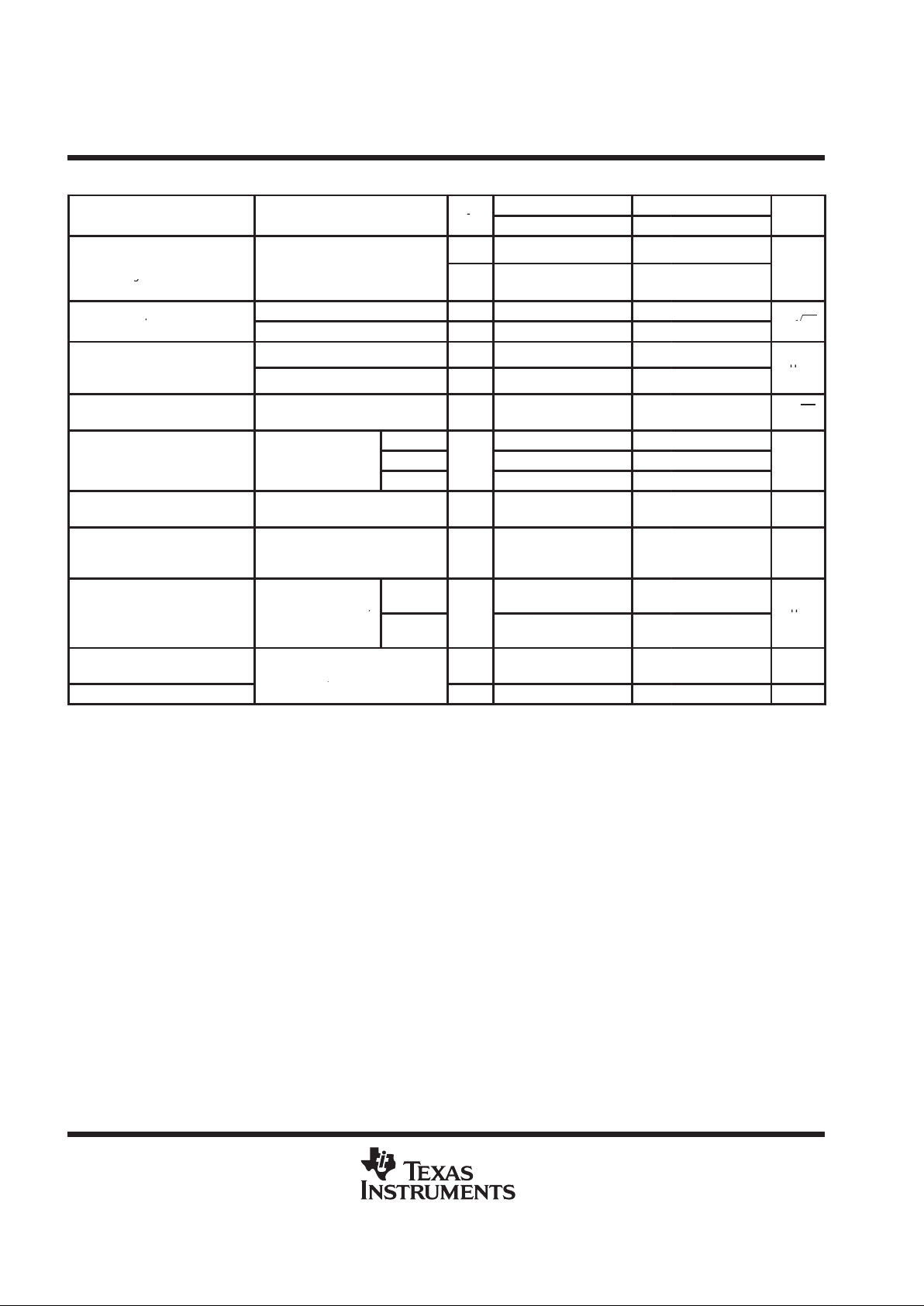
TLC2274C electrical characteristics at specified free-air temperature, V
DD
= 5 V (unless otherwise
noted)
TLC2274C TLC2274AC
PARAMETER
TEST
CONDITIONS
T
A
†
MIN TYP MAX MIN TYP MAX
UNIT
p
25°C 300 2500 300 950
V
IO
Inp
u
t
offset
v
oltage
Full range 3000 1500
µ
V
α
VIO
T emperature coef ficient
of input offset voltage
25°C
to 70°C
2 2 µV/°C
Input offset voltage
long-term drift
(see Note 4)
V
DD±
= ±2.5 V,
V
O
= 0,
V
IC
= 0,
R
S
= 50 Ω
25°C
0.002 0.002 µV/mo
p
25°C 0.5 0.5
p
I
IO
Inp
u
t
offset
c
u
rrent
Full range 100 100
pA
p
25°C 1 1
p
I
IB
Inp
u
t
bias
c
u
rrent
Full range 100 100
pA
Common-mode input
25°C
0
to
4
–0.3
to
4.2
0
to
4
–0.3
to
4.2
V
ICR
voltage range
R
S
=
50Ω
,
V
IO
≤
5
m
V
,
Full range
0
to
3.5
0
to
3.5
V
I
OH
= –20 µA 25°C 4.99 4.99
25°C 4.85 4.93 4.85 4.93
V
OH
Hi
g
h
-
l
eve
l
ou
t
pu
t
I
OH
= –
200
µ
A
Full range 4.85 4.85
V
voltage
25°C 4.25 4.65 4.25 4.65
I
OH
= –
1
mA
Full range 4.25 4.25
V
IC
= 2.5 V, I
OL
= 50 µA 25°C 0.01 0.01
V
IC
= 2.5 V,
25°C 0.09 0.15 0.09 0.15
V
OL
L
ow-
l
eve
l
ou
t
pu
t
IC
I
OL
= 500 µA
Full range 0.15 0.15
V
voltage
25°C 0.9 1.5 0.9 1.5
V
IC
=
2
.
5
V
,
I
OL
=
5
m
A
Full range 1.5 1.5
25°C 15 35 15 35
A
VD
L
arge-s
i
gna
l
diff
eren
ti
a
l
p
V
IC
=
2
.
5
V
,
R
L
=
10
kΩ
‡
Full range 15 15
V/mV
VD
voltage
am lification
V
O
=
1
V
to
4
V
R
L
= 1 mΩ
‡
25°C 175 175
r
id
Differential input
resistance
25°C 10
12
10
12
Ω
r
i
Common-mode input
resistance
25°C 10
12
10
12
Ω
c
i
Common-mode input
capacitance
f = 10 kHz, N package 25°C 8 8 pF
z
o
Closed-loop output
impedance
f = 1 MHz, A
V
= 10 25°C 140 140
Ω
Common-mode V
IC
= 0 to 2.7 V,
25°C 70 75 70 75
CMRR
rejection ratio
IC
V
O
= 2.5 V, R
S
= 50Ω
Full range 70 70
dB
Supply-voltage rejection V
DD
= 4.4 V to 16 V,
25°C 80 95 80 95
k
SVR
ygj
ratio (∆V
DD
/∆V
IO
)
DD
V
IC
= V
DD
/2, No load
Full range 80 80
dB
pp
25°C 4.4 6 4.4 6
I
DD
S
u
ppl
y
c
u
rrent
V
O
=
2
.
5
V
,
No
load
Full range 6 6
mA
†
Full range is 0°C to 70°C.
‡
Referenced to 2.5 V
NOTE 4: T ypical values are based on the input offset voltage shift observed through 168 hours of operating life test at T
A
= 150°C extrapolated
to T
A
= 25°C using the Arrhenius equation and assuming an activation energy of 0.96 eV .
TLC227x, TLC227xA
Advanced LinCMOS RAIL-TO-RAIL
OPERATIONAL AMPLIFIERS
SLOS190B – FEBRUARY 1997 – REVISED JULY 1999
10
POST OFFICE BOX 655303 • DALLAS, TEXAS 75265
TLC2274C operating characteristics at specified free-air temperature, V
DD
= 5 V
TLC2274C TLC2274AC
PARAMETER
TEST
CONDITIONS
T
A
†
MIN TYP MAX MIN TYP MAX
UNIT
25°C 2.3 3.6 2.3 3.6
SR
Sle
w
rate
at
V
O
=
0
.
5
V
t
o
2
.
5
V
,
‡
p
‡
Full
V/µs
unity
gain
R
L
=
10
kΩ
‡
,
C
L
=
100
F
‡
range
1
.
7
1
.
7
Equivalent input
f = 10 Hz 25°C 50 50
V
n
q
noise voltage
f = 1 kHz
25°C 9 9
n
V/√H
z
Peak-to-peak
p
f = 0.1 to 1 Hz 25°C 1 1
V
N(PP)
equ
i
va
l
en
t
i
npu
t
noise voltage
f = 0.1 to 10 Hz
25°C 1.4 1.4
µ
V
I
n
Equivalent input
noise current
25°C 0.6 0.6
fA/√Hz
=
A
V
= 1 0.0013% 0.0013%
THD + N
Total
harmonic
distortion plus
V
O
=
0
.
5
V
to
2
.
5
V
,
f = 20 kHz,
A
V
= 10
25°C
0.004% 0.004%
noise R
L
= 10 kΩ
‡
A
V
= 100 0.03% 0.03%
Gain-bandwidth
product
f = 10 kHz,
C
L
= 100 pF
‡
R
L
= 10 kΩ
‡
,
25°C 2.18 2.18 MHz
B
OM
Maximum
output-swing
bandwidth
V
O(PP)
= 2 V,
R
L
= 10 kΩ
‡
,
A
V
= 1,
C
L
= 100 pF
‡
25°C 1 1 MHz
A
= –1
,
A
V
=
1
,
Step = 0.5 V to 2.5 V ,
To
0
.
1%
°
1
.
5
1
.
5
t
s
Settling
time
,
R
L
= 10 kΩ
‡
,
25°C
µ
s
C
L
= 100 pF
‡
To
0
.
01%
2
.
6
2
.
6
φ
m
Phase margin at
unity gain
R
= 10 kΩ
‡
, C
= 100 pF
‡
25°C 50° 50°
Gain margin
L
,
L
25°C 10 10 dB
†
Full range is 0°C to 70°C.
‡
Referenced to 2.5 V
TLC227x, TLC227xA
Advanced LinCMOS RAIL-TO-RAIL
OPERATIONAL AMPLIFIERS
SLOS190B – FEBRUARY 1997 – REVISED JULY 1999
11
POST OFFICE BOX 655303 • DALLAS, TEXAS 75265
TLC2274C electrical characteristics at specified free-air temperature, V
DD±
= ±5 V (unless
otherwise noted)
TLC2274C TLC2274AC
PARAMETER
TEST
CONDITIONS
T
A
†
MIN TYP MAX MIN TYP MAX
UNIT
p
25°C 300 2500 300 950
V
IO
Inp
u
t
offset
v
oltage
Full range 3000 1500
µ
V
Temperature coefficient of input 25°C
°
α
VIO
offset voltage to 70°C
2
2
µ
V/°C
Input offset voltage long-term
drift (see Note 4)
V
IC
= 0,
R
S
= 50 Ω
V
O
= 0,
25°C
0.002 0.002 µV/mo
p
25°C 0.5 0.5
p
I
IO
Inp
u
t
offset
c
u
rrent
Full range 100 100
pA
p
25°C 1 1
p
I
IB
Inp
u
t
bias
c
u
rrent
Full range 100 100
pA
Common-mode input
25°C
–5
to
4
–5.3
to
4.2
–5
to
4
–5.3
to
4.2
V
ICR
voltage range
R
S
=
50
Ω
,
|V
IO
|
≤
5
mV
Full range
–5
to
3.5
–5
to
3.5
V
I
O
= –20 µA 25°C 4.99 4.99
25°C 4.85 4.93 4.85 4.93
V
OM+
M
ax
i
mum pos
iti
ve pea
k
ou
t
pu
t
I
O
= –
200
µ
A
Full range 4.85 4.85
V
voltage
25°C 4.25 4.65 4.25 4.65
I
O
= –
1
mA
Full range 4.25 4.25
V
IC
= 0, I
O
= 50 µA 25°C
–4.9
9
–4.9
9
Maximum ne
g
ative peak output
25°C
–4.8
5
–4.9
1
–4.8
5
–4.9
1
V
OM–
Maximum
negative
eak
out ut
voltage
V
IC
=
0
,
I
O
=
500
µ
A
Full range
–4.8
5
–4.8
5
V
25°C –3.5 –4.1 –3.5 –4.1
V
IC
=
0
,
I
O
= –
5
mA
Full range –3.5 –3.5
25°C 25 50 25 50
A
VD
L
arge-s
i
gna
l
diff
eren
ti
a
l
vo
lt
age
p
V
O
= ±4 V
R
L
=
10
kΩ
Full range 25 25
V/mV
am lification
R
L
= 1 MΩ 25°C 300 300
r
id
Differential input resistance 25°C 10
12
10
12
Ω
r
i
Common-mode input resistance 25°C 10
12
10
12
Ω
c
i
Common-mode input
capacitance
f = 10 kHz, N package 25°C 8 8 pF
z
o
Closed-loop output impedance f = 1 MHz, A
V
= 10 25°C 130 130
Ω
V
IC
= –5 V to 2.7 V,
25°C 75 80 75 80
CMRR
Common
-
mode
rejection
ratio
IC
V
O
= 0, R
S
= 50 Ω
Full range 75 75
dB
Supply-voltage rejection ratio V
DD±
= ±2.2 V to ±8 V,
25°C 80 95 80 95
k
SVR
ygj
(∆V
DD±
/∆V
IO
)
DD±
V
IC
= 0, No load
Full range 80 80
dB
pp
25°C 4.8 6 4.8 6
I
DD
S
u
ppl
y
c
u
rrent
V
O
=
0
,
No
load
Full range 6 6
mA
†
Full range is 0°C to 70°C.
NOTE 4: T ypical values are based on the input offset voltage shift observed through 168 hours of operating life test at T
A
= 150°C extrapolated
to T
A
= 25°C using the Arrhenius equation and assuming an activation energy of 0.96 eV .

TLC227x, TLC227xA
Advanced LinCMOS RAIL-TO-RAIL
OPERATIONAL AMPLIFIERS
SLOS190B – FEBRUARY 1997 – REVISED JULY 1999
12
POST OFFICE BOX 655303 • DALLAS, TEXAS 75265
TLC2274C operating characteristics at specified free-air temperature, V
DD±
= ±5 V
TLC2274C TLC2274AC
PARAMETER
TEST
CONDITIONS
T
A
†
MIN TYP MAX MIN TYP MAX
UNIT
25°C 2.3 3.6 2.3 3.6
SR
Sle
w
rate
at
u
nit
y
V
O
=
±2
.
3
V
,
=
p
R
L
=
10
kΩ
,
Full
V/µs
gain
C
L
=
100
F
range
1
.
7
1
.
7
Equivalent input
f = 10 Hz 25°C 50 50
V
n
q
noise voltage
f = 1 Hz
25°C 9 9
n
V/√H
z
Peak-to-peak
p
f = 0.1 Hz to 1 Hz 25°C 1 1
V
N(PP)
equ
i
va
l
en
t
i
npu
t
noise voltage
f = 0.1 Hz to 10 Hz
25°C 1.4 1.4
µ
V
I
n
Equivalent input
noise current
25°C 0.6 0.6
fA/√Hz
=
A
V
= 1 0.0011% 0.0011%
THD + N
Total
harmonic
distortion plus
V
O
=
±2
.
3
V
,
f = 20 kHz,
A
V
= 10
25°C
0.004% 0.004%
noise R
L
= 10 kΩ
A
V
= 100 0.03% 0.03%
Gain-bandwidth f = 10 kHz, R
= 10 kΩ,
°
product
,
C
L
= 100 pF
L
,
25°C
2
.
25
2
.
25
MH
z
Maximum
p
V
O
(
PP
)
= 4.6 V, A
V
= 1,
°
B
OM
ou
t
pu
t
-sw
i
ng
bandwidth
O(PP)
R
L
= 10 kΩ,
V
C
L
= 100 pF
25°C
0
.
54
0
.
54
MH
z
=–
A
V
=
1
,
Step = –2.3 V to 2.3 V,
To
0
.
1%
°
1
.
5
1
.
5
t
s
Settling
time
,
R
L
= 10 kΩ,
25°C
µ
s
L
C
L
= 100 pF
To
0
.
01%
3
.
2
3
.
2
φ
m
Phase margin at
unity gain
R
L
= 10 kΩ, C
L
= 100 pF
25°C 52° 52°
Gain margin
L
L
25°C 10 10 dB
†
Full range is 0°C to 70°C.

TLC227x, TLC227xA
Advanced LinCMOS RAIL-TO-RAIL
OPERATIONAL AMPLIFIERS
SLOS190B – FEBRUARY 1997 – REVISED JULY 1999
13
POST OFFICE BOX 655303 • DALLAS, TEXAS 75265
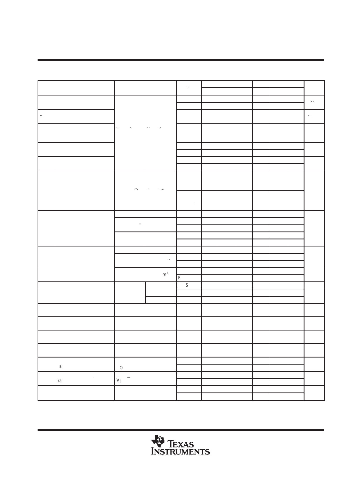
TLC2272I electrical characteristics at specified free-air temperature, V
DD
= 5 V (unless otherwise
noted)
TLC2272I TLC2272AI
PARAMETER
TEST
CONDITIONS
T
A
†
MIN TYP MAX MIN TYP MAX
UNIT
p
25°C 300 2500 300 950
V
IO
Inp
u
t
offset
v
oltage
Full range 3000 1500
µ
V
T emperature coef ficient
25°C
°
α
VIO
of input offset voltage
to 85°C
2
2
µ
V/°C
Input offset voltage
long-term drift
(see Note 4)
V
IC
=
0
,
V
O
= 0,
V
DD±
=
±2
.
5V
R
S
= 50 Ω
25°C 0.002 0.002 µV/mo
p
25°C 0.5 0.5
p
I
IO
Inp
u
t
offset
c
u
rrent
Full range 150 150
pA
p
25°C 1 1
p
I
IB
Inp
u
t
bias
c
u
rrent
Full range 150 150
pA
0 –0.3 0 –0.3
25°C
to to to to
Common-mode input
4 4.2 4 4.2
V
ICR
voltage range R
S
= 50 Ω, |V
IO
| ≤5 mV
0 0
V
Full range
to to
g
3.5 3.5
I
OH
= –20 µA 25°C 4.99 4.99
25°C 4.85 4.93 4.85 4.93
V
OH
Hi
g
h
-
l
eve
l
ou
t
pu
t
I
OH
= –
200
µ
A
Full range 4.85 4.85
V
voltage
25°C 4.25 4.65 4.25 4.65
I
OH
= –
1
mA
Full range 4.25 4.25
V
IC
= 2.5 V, I
OL
= 50 µA 25°C 0.01 0.01
25°C 0.09 0.15 0.09 0.15
V
OL
L
ow-
l
eve
l
ou
t
pu
t
V
IC
=
2
.
5
V
,
I
OL
=
500
µ
A
Full range 0.15 0.15
V
voltage
25°C 0.9 1.5 0.9 1.5
V
IC
=
2
.
5
V
,
I
OL
=
5
m
A
Full range 1.5 1.5
25°C 15 35 15 35
A
VD
L
arge-s
i
gna
l
diff
eren
ti
a
l
p
V
IC
=
2
.
5
V
,
R
L
=
10
kΩ
‡
Full range 15 15
V/mV
VD
voltage
am lification
V
O
=
1
V
to
4
V
R
L
= 1 mΩ
‡
25°C 175 175
r
id
Differential input
resistance
25°C 10
12
10
12
Ω
r
i
Common-mode input
resistance
25°C 10
12
10
12
Ω
c
i
Common-mode input
capacitance
f = 10 kHz, P package 25°C 8 8 pF
z
o
Closed-loop output
impedance
f = 1 MHz, A
V
= 10 25°C 140 140
Ω
Common-mode V
IC
= 0 to 2.7 V,
25°C 70 75 70 75
CMRR
rejection ratio
IC
V
O
= 2.5 V, R
S
= 50 Ω
Full range 70 70
dB
Supply-voltage rejection V
DD
= 4.4 V to 16 V,
25°C 80 95 80 95
k
SVR
ygj
ratio (∆V
DD
/∆V
IO
)
DD
V
IC
= V
DD
/2, No load
Full range 80 80
dB
pp
25°C 2.2 3 2.2 3
I
DD
S
u
ppl
y
c
u
rrent
V
O
=
2
.
5
V
,
No
load
Full range 3 3
mA
†
Full range is – 40°C to 85°C.
‡
Referenced to 2.5 V
NOTE 4: T ypical values are based on the input offset voltage shift observed through 168 hours of operating life test at T
A
= 150°C extrapolated
to T
A
= 25°C using the Arrhenius equation and assuming an activation energy of 0.96 eV .
TLC227x, TLC227xA
Advanced LinCMOS RAIL-TO-RAIL
OPERATIONAL AMPLIFIERS
SLOS190B – FEBRUARY 1997 – REVISED JULY 1999
14
POST OFFICE BOX 655303 • DALLAS, TEXAS 75265
TLC2272I operating characteristics at specified free-air temperature, V
DD
= 5 V
TLC2272I TLC2272AI
PARAMETER
TEST
CONDITIONS
T
A
†
MIN TYP MAX MIN TYP MAX
UNIT
25°C
2.3 3.6 2.3 3.6
SR
Sle
w
rate
at
V
O
=
0
.
5
V
to
2
.
5
V
,
=
‡
=
p
‡
Full
V/µs
unity
gain
R
L
=
10
kΩ
‡
,
C
L
=
100
F
‡
range
1
.
7
1
.
7
Equivalent input
f = 10 Hz 25°C 50 50
V
n
q
noise voltage
f = 1 kHz
25°C 9 9
n
V√H
z
Peak-to-peak
p
f = 0.1 Hz to 1 Hz 25°C 1 1
V
NPP
equ
i
va
l
en
t
i
npu
t
noise voltage
f = 0.1 Hz to 10 Hz
25°C 1.4 1.4
µ
V
I
n
Equivalent input
noise current
25°C 0.6 0.6
fA√Hz
=
A
V
= 1 0.0013% 0.0013%
THD + N
Total
harmonic
distortion plus
V
O
=
0
.
5
V
to
2
.
5
V
,
f = 20 kHz,
A
V
= 10
25°C
0.004% 0.004%
noise R
L
= 10 kΩ
‡
A
V
= 100 0.03% 0.03%
Gain-bandwidth
f = 10 kHz, R
= 10 kΩ
‡
,
°
product
,
C
L
= 100 pF
‡
L
,
25°C
2
.
18
2
.
18
MH
z
Maximum output- V
= 2 V, A
= 1,
°
B
OM
swing bandwidth
O(PP)
,
R
L
= 10 kΩ
‡
,
V
,
C
L
= 100 pF
‡
25°C
1
1
MH
z
–
A
V
=
–1
,
Step = 0.5 V to 2.5 V
,
To
0
.
1%
1
.
5
1
.
5
t
s
S
e
ttli
ng
ti
me
Ste
0.5
V
to
2.5
V,
R
L
= 10 kΩ
‡
,
To
25°C
µs
L
C
L
= 100 pF
‡
0.01%
2
.
6
2
.
6
φ
m
Phase margin at
unity gain
R
= 10 kΩ
‡
, C
= 100 pF
‡
25°C
50° 50°
Gain margin
L
,
L
25°C 10 10 dB
†
Full range is – 40°C to 85°C.
‡
Referenced to 2.5 V
TLC227x, TLC227xA
Advanced LinCMOS RAIL-TO-RAIL
OPERATIONAL AMPLIFIERS
SLOS190B – FEBRUARY 1997 – REVISED JULY 1999
15
POST OFFICE BOX 655303 • DALLAS, TEXAS 75265
TLC2272I electrical characteristics at specified free-air temperature, V
DD±
= ±5 V (unless otherwise
noted)
TLC2272I TLC2272AI
PARAMETER
TEST
CONDITIONS
T
A
†
MIN TYP MAX MIN TYP MAX
UNIT
p
25°C 300 2500 300 950
V
IO
Inp
u
t
offset
v
oltage
Full range 3000 1500
µ
V
α
VIO
T emperature coef ficient
of input offset voltage
25°C
to 85°C
2 2 µV/°C
Input offset voltage
long-term drift
(see Note 4)
V
IC
= 0,
R
S
= 50 Ω
V
O
= 0,
25°C
0.002 0.002 µV/mo
p
25°C 0.5 0.5
p
I
IO
Inp
u
t
offset
c
u
rrent
Full range 150 150
pA
p
25°C 1 1
p
I
IB
Inp
u
t
bias
c
u
rrent
Full range 150 150
pA
Common-mode input
25°C
–5
to
4
–5.3
to
4.2
–5
to
4
–5.3
to
4.2
V
ICR
voltage range
R
S
=
50
Ω
,
|V
IO
|
≤5
mV
Full range
–5
to
3.5
–5
to
3.5
V
I
O
= –20 µA 25°C 4.99 4.99
25°C 4.85 4.93 4.85 4.93
V
OM+
M
ax
i
mum pos
iti
ve pea
k
p
I
O
= –
200
µ
A
Full range 4.85 4.85
V
out ut
voltage
25°C 4.25 4.65 4.25 4.65
I
O
= –
1
mA
Full range 4.25 4.25
V
IC
= 0, I
O
= 50 µA 25°C –4.99 –4.99
25°C –4.85 –4.91 –4.85 –4.91
V
OM–
M
ax
i
mum nega
ti
ve
p
p
V
IC
=
0
,
I
O
=
500
µ
A
Full range –4.85 –4.85
V
eak
out ut
voltage
25°C –3.5 –4.1 –3.5 –4.1
V
IC
=
0
,
I
O
=
5
m
A
Full range –3.5 –3.5
Lar
g
e-si
g
nal
25°C 25 50 25 50
A
VD
Large signal
differential voltage
V
O
= ±4 V
R
L
=
10
kΩ
Full range 25 25
V/mV
amplification
R
L
= 1 mΩ 25°C 300 300
r
id
Differential input
resistance
25°C 10
12
10
12
Ω
r
i
Common-mode input
resistance
25°C 10
12
10
12
Ω
c
i
Common-mode input
capacitance
f = 10 kHz, P package 25°C 8 8 pF
z
o
Closed-loop output
impedance
f = 1 MHz, A
V
= 10 25°C 130 130
Ω
Common-mode
V
= 0 to 2.7 V,
25°C 75 80 75 80
CMRR
rejection ratio
IC
,
V
O
= 2.5 V, R
S
= 50 Ω
Full range 75 75
dB
Supply-voltage
V
DD
= 4.4 V to 16 V,
25°C 80 95 80 95
k
SVR
rejection
ratio
(∆V
DD±
/∆V
IO
)
DD
,
V
IC
= V
DD
/2, No load
Full range 80 80
dB
pp
25°C 2.4 3 2.4 3
I
DD
S
u
ppl
y
c
u
rrent
V
O
=
2
.
5
V
,
No
load
Full range 3 3
mA
†
Full range is – 40°C to 85°C.
NOTE 4: T ypical values are based on the input offset voltage shift observed through 168 hours of operating life test at T
A
= 150°C extrapolated
to T
A
= 25°C using the Arrhenius equation and assuming an activation energy of 0.96 eV .

TLC227x, TLC227xA
Advanced LinCMOS RAIL-TO-RAIL
OPERATIONAL AMPLIFIERS
SLOS190B – FEBRUARY 1997 – REVISED JULY 1999
16
POST OFFICE BOX 655303 • DALLAS, TEXAS 75265
TLC2272I operating characteristics at specified free-air temperature, V
DD±
= ±5 V
TLC2272I TLC2272AI
PARAMETER
TEST
CONDITIONS
T
A
†
MIN TYP MAX MIN TYP MAX
UNIT
25°C 2.3 3.6 2.3 3.6
SR
Slew
rate
at
unit
y
g
ain
V
O
=
±2
.
3
V
,
C
= 100 pF
R
L
=
10
kΩ
,
Full
V/µs
yg
C
L
100
F
range
1
.
7
1
.
7
Equivalent input
f = 10 Hz 25°C 50 50
V
n
q
noise voltage
f = 1 kHz
25°C 9 9
n
V√H
z
Peak-to-peak
p
f = 0.1 Hz to 1 Hz 25°C 1 1
V
NPP
equ
i
va
l
en
t
i
npu
t
noise voltage
f = 0.1 Hz to 10 Hz
25°C 1.4 1.4
µ
V
I
n
Equivalent input
noise current
25°C 0.6 0.6
fA√Hz
=
A
V
= 1 0.0011% 0.0011%
THD + N
Total
harmonic
distortion plus
V
O
=
±2
.
3
V
R
L
= 10 kΩ,
A
V
= 10
25°C
0.004% 0.004%
noise f = 20 kHz
A
V
= 100 0.03% 0.03%
Gain-bandwidth f =10 kHz, R
= 10 kΩ,
°
product
,
C
L
= 100 pF
L
,
25°C
2
.
25
2
.
25
MH
z
Maximum
p
V
= 4.6 V, A
= 1,
°
B
OM
ou
t
pu
t
-sw
i
ng
bandwidth
O(PP)
,
R
L
= 10 kΩ,
V
,
C
L
= 100 pF
25°C
0
.
54
0
.
54
MH
z
=–
A
V
=
1
,
Step = –2.3 V to 2.3 V,
To
0
.
1%
°
1
.
5
1
.
5
t
s
Settling
time
,
R
L
= 10 kΩ,
25°C
µ
s
L
C
L
= 100 pF
To
0
.
01%
3
.
2
3
.
2
φ
m
Phase margin at
unity gain
R
L
= 10 kΩ, C
L
= 100 pF
25°C
52° 52°
Gain margin
L
L
25°C 10 10 dB
†
Full range is –40°C to 85°C.
 Loading...