Texas Instruments TLC876IPWR, TLC876IPWLE, TLC876IPW, TLC876IDW, TLC876IDWR Datasheet
...
|
TLC876M, TLC876I, TLC876C |
|
|
10-BIT 20 MSPS PARALLEL OUTPUT CMOS |
|
|
ANALOG-TO-DIGITAL CONVERTERS |
|
|
SLAS140D ± JULY 1997 ± REVISED MAY 2000 |
|
|
|
|
D 10-Bit Resolution 20 MSPS Sampling |
DB, DW, OR PW PACKAGE |
|
Analog-to-Digital Converter (ADC) |
(TOP VIEW) |
|
DPower Dissipation . . . 107 mW Typ
D5-V Single Supply Operation
DDifferential Nonlinearity . . . ±0.5 LSB Typ
DNo Missing Codes
DPower Down (Standby) Mode
DThree State Outputs
DDigital I/Os Compatible With 5-V or 3.3-V Logic
DAdjustable Reference Input
DSmall Outline Package (SOIC), Super Small Outline Package (SSOP), or Thin Small Outline Package (TSOP)
DPin Compatible With the Analog
Devices AD876
AGND |
|
1 |
28 |
|
|
AVDD |
|
|
|
|
|||||
DRVDD |
|
2 |
27 |
|
|
AIN |
|
|
|
|
|||||
D0 |
|
3 |
26 |
|
|
CML |
|
|
|
|
|||||
D1 |
|
4 |
25 |
|
|
REFBS |
|
|
|
|
|||||
D2 |
|
5 |
24 |
|
|
REFBF |
|
|
|
|
|||||
D3 |
|
6 |
23 |
|
|
NC |
|
|
|
|
|||||
D4 |
|
7 |
22 |
|
|
REFTF |
|
|
|
|
|||||
D5 |
|
8 |
21 |
|
|
REFTS |
|
|
|
|
|||||
D6 |
|
9 |
20 |
|
|
DGND |
|
|
|
|
|||||
D7 |
|
10 |
19 |
|
|
AGND |
|
|
|
|
|||||
D8 |
|
11 |
18 |
|
|
DVDD |
|
|
|
|
|||||
D9 |
|
12 |
17 |
|
|
STBY |
|
|
|
|
|||||
DRGND |
|
13 |
16 |
|
|
OE |
|
|
|
|
|
||||
DGND |
|
14 |
15 |
|
|
CLK |
|
|
|
|
|||||
|
|
|
|
|
|
|
|
applications |
NC ± No internal connection |
|
DCommunications
DMultimedia
DDigital Video Systems
DHigh-Speed DSP Front-End . . . TMS320C6x
description
The TLC876 is a CMOS, low-power, 10-bit, 20 MSPS analog-to-digital converter (ADC). The speed, resolution, and single-supply operation are suited for applications in video, multimedia, imaging, high-speed acquisition, and communications. The low-power and single-supply operation satisfy requirements for high-speed portable applications. The speed and resolution ideally suit charge-coupled device (CCD) input systems such as color scanners, digital copiers, electronic still cameras, and camcorders. A multistage pipelined architecture with output error correction logic provides for no missing codes over the full operating temperature range. Force and sense connections to the reference inputs provide a more accurate internal reference voltage to the reference resistor string.
A standby mode of operation reduces the power to typically 15 mW. The digital I/O interfaces to either 5-V or 3.3-V logic and the digital output terminals can be placed in a high-impedance state. The format of the output data is straight binary coding.
A pipelined multistaged architecture achieves a high sample rate with low power consumption. The TLC876 distributes the conversion over several smaller ADC sub-blocks, refining the conversion with progressively higher accuracy as the device passes the results from stage to stage. This distributed conversion requires a small fraction of the 1023 comparators used in a traditional flash ADC. A sample-and-hold amplifier (SHA) within each of the stages permits the first stage to operate on a new input sample while the second through the fifth stages operate on the four preceding samples.
Please be aware that an important notice concerning availability, standard warranty, and use in critical applications of Texas Instruments semiconductor products and disclaimers thereto appears at the end of this data sheet.
PRODUCTION DATA information is current as of publication date. Products conform to specifications per the terms of Texas Instruments standard warranty. Production processing does not necessarily include testing of all parameters.
Copyright 1999, Texas Instruments Incorporated
On products compliant to MIL-PRF-38535, all parameters are tested unless otherwise noted. On all other products, production processing does not necessarily include testing of all parameters.
POST OFFICE BOX 655303 •DALLAS, TEXAS 75265 |
1 |

TLC876M, TLC876I, TLC876C
10-BIT 20 MSPS PARALLEL OUTPUT CMOS ANALOG-TO-DIGITAL CONVERTERS
SLAS140D ± JULY 1997 ± REVISED MAY 2000
description (continued)
The TLC876C is characterized for operation from 0°C to 70°C, the TLC876I is characterized for operation from ±40°C to 85°C, and the TLC876M is characterized for operation over the full military temperature range of ±55°C to 125°C.
AVAILABLE OPTIONS
|
|
PACKAGE |
|
|
|
|
|
|
|
TA |
SUPER SMALL |
SMALL |
TSSOP |
|
OUTLINE |
OUTLINE |
|||
|
(PW) |
|||
|
(DB) |
(DW) |
||
|
|
|||
|
|
|
|
|
0°C to 70°C |
TLC876CDB |
TLC876CDW |
TLC876CPW |
|
|
|
|
|
|
±40°C to 85°C |
TLC876IDB |
TLC876IDW |
TLC876IPW |
|
|
|
|
|
|
±55°C to 125°C |
Ð |
TLC876MDW |
Ð |
|
|
|
|
|
functional block diagram
SHA² |
SHA² |
GAIN |
SHA² |
|
GAIN |
SHA² |
GAIN |
SHA² |
GAIN |
||
27 |
|
|
|
|
|
|
|
|
|
|
ADC |
AIN |
|
|
|
|
|
|
|
|
|
|
|
|
ADC |
DAC |
|
ADC |
DAC |
|
ADC |
DAC |
ADC |
DAC |
|
|
|
2 |
|
2 |
|
|
2 |
|
2 |
2 |
|
Correction Logic
10 |
|
Output Buffers |
12 |
(MSB) D9
10 |
3 |
|
(LSB) D0 |
² Sample and hold amplifier
2 |
POST OFFICE BOX 655303 •DALLAS, TEXAS 75265 |
TLC876M, TLC876I, TLC876C 10-BIT 20 MSPS PARALLEL OUTPUT CMOS ANALOG-TO-DIGITAL CONVERTERS
SLAS140D ± JULY 1997 ± REVISED MAY 2000
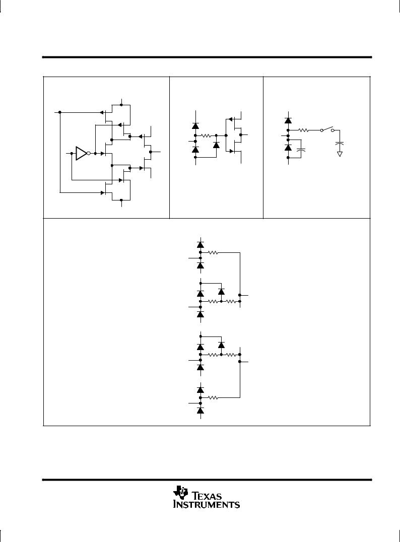
equivalent input and output circuits
D0±D9 OUTPUT CIRCUIT |
ALL DIGITAL INPUT CIRCUITS |
AIN INPUT CIRCUIT |
|
|
DVDD |
|
|
|
|
|
DVDD |
DRVDD |
AVDD |
|
|
DRVDD |
|
30 Ω typ |
|
|
CLK |
|
AIN |
0.5 pF typ |
|
|
|
||
|
|
|
|
|
|
D0±D9 |
|
0.3 pF |
|
|
|
|
|
|
|
DGND |
DRGND |
AGND |
|
|
DRGND |
|
|
|
DGND |
|
|
|
|
|
REFERENCE INPUT CIRCUIT |
|
|
|
|
AVDD |
|
|
|
|
30 |
|
|
|
|
REFTF |
|
|
|
|
AVDD |
AVSS |
|
|
|
|
|
|
|
|
|
Internal Reference |
|
|
|
29 |
Voltage |
|
|
|
|
|
|
|
|
REFTS |
|
|
|
|
|
AGND |
|
|
|
AVDD |
|
|
|
REFBS |
35 |
Internal Reference |
|
||
|
Voltage |
|
|
|
AVSS
AVDD |
34 |
REFBF |
AGND |
POST OFFICE BOX 655303 •DALLAS, TEXAS 75265 |
3 |

TLC876M, TLC876I, TLC876C
10-BIT 20 MSPS PARALLEL OUTPUT CMOS ANALOG-TO-DIGITAL CONVERTERS
SLAS140D ± JULY 1997 ± REVISED MAY 2000
|
|
|
|
|
|
|
Terminal Functions |
||
|
|
|
|
|
|
|
|
|
|
|
|
TERMINAL |
I/O |
|
|
DESCRIPTION |
|||
|
NAME |
NO. |
|
|
|||||
|
|
|
|
|
|
|
|||
|
|
|
|
|
|
|
|
|
|
|
AGND |
1, 19 |
|
Analog ground |
|||||
|
|
|
|
|
|
|
|
|
|
|
AIN |
27 |
I |
Analog input |
|||||
|
|
|
|
|
|
|
|
|
|
|
AVDD |
28 |
|
5-V analog supply |
|||||
|
CLK |
15 |
I |
Clock input |
|||||
|
|
|
|
|
|
|
|
|
|
|
CML |
26 |
O |
Bypass for an internal bias point. Typically a 0.1 F capacitor minimum is connected from this terminal to ground. |
|||||
|
|
|
|
|
|
|
|
|
|
|
DGND |
14, 20 |
|
Digital ground |
|||||
|
|
|
|
|
|
|
|
|
|
|
DVDD |
18 |
|
5-V digital supply |
|||||
|
DRVDD |
2 |
|
3.3-V/5-V digital supply. Supply for digital input and output buffers. |
|||||
|
DRGND |
13 |
|
3.3-V/5-V digital ground. Ground for digital input and output buffers. |
|||||
|
|
|
|
|
|
|
|
|
|
|
D0 ±D9 |
3 ± 12 |
O |
Digital data out. D0:LSB, D9:MSB |
|||||
|
|
|
|
|
|
|
|
|
|
|
|
|
16 |
I |
Output enable. When |
|
= low or NC, the device is in normal operating mode. When |
|
= high, D0±D9 are high |
|
OE |
|
OE |
OE |
|||||
|
|
|
|
|
impedance. |
||||
|
|
|
|
|
|||||
|
REFBF |
24 |
I |
Reference bottom force |
|||||
|
|
|
|
|
|||||
|
REFBS |
25 |
I |
Reference bottom sense |
|||||
|
|
|
|
|
|||||
|
REFTF |
22 |
I |
Reference top force |
|||||
|
|
|
|
|
|||||
|
REFTS |
21 |
I |
Reference top sense |
|||||
|
|
|
|
|
|||||
|
STBY |
17 |
I |
Standby enable. When STBY = low or NC, the device is in normal operating mode. When STBY = high, the device |
|||||
|
|
|
|
|
is in standby mode. |
||||
|
|
|
|
|
|
|
|
|
|
4 |
POST OFFICE BOX 655303 •DALLAS, TEXAS 75265 |

TLC876M, TLC876I, TLC876C 10-BIT 20 MSPS PARALLEL OUTPUT CMOS ANALOG-TO-DIGITAL CONVERTERS
SLAS140D ± JULY 1997 ± REVISED MAY 2000
absolute maximum ratings over operating free-air temperature range (unless otherwise noted)²
Supply voltage, AVDD to AGND, DVDD to DGND . . . . . . . . . . . . . . . . . . . . . . . . . . . . . . . |
. . . . . . . ±0.3 V to 6.5 V |
|
Reference voltage input range to AGND, VI(REFTF), |
|
|
VI(REFBF), VI(REFBS), VI(REFTS) . . . . . . . . . . . . . . . . . . . . . . . . . . . . . . . . . . . . . . . . . . . |
±0.3 V to AVDD + 0.3 |
V |
Analog input voltage range to AGND . . . . . . . . . . . . . . . . . . . . . . . . . . . . . . . . . . . . . . . . |
±0.3 V to AVDD + 0.3 |
V |
Digital input voltage range . . . . . . . . . . . . . . . . . . . . . . . . . . . . . . . . . . . . . . . . . . . . . . . . . |
±0.3 V to DVDD + 0.3 |
V |
Digital output voltage range applied from external source . . . . . . . . . . . . . . . . . . . . . . . |
. . . . . . ±0.5 V to DVDD |
|
Operating virtual junction temperature range, TJ . . . . . . . . . . . . . . . . . . . . . . . . . . . . . . . |
. . . . . . ±55°C to 150°C |
|
Operating free-air temperature range, TA: TLC876C . . . . . . . . . . . . . . . . . . . . . . . . . . . . |
. . . . . . . . . 0°C to 70°C |
|
TLC876I . . . . . . . . . . . . . . . . . . . . . . . . . . . . . |
. . . . . . . ±40°C to 85°C |
|
TLC876M . . . . . . . . . . . . . . . . . . . . . . . . . . . |
. . . . . . ±55°C to 125°C |
|
Storage temperature range, Tstg . . . . . . . . . . . . . . . . . . . . . . . . . . . . . . . . . . . . . . . . . . . . . |
. . . . . . ±65°C to 150°C |
|
Lead temperature 1,6 mm (1/16 inch) from case for 10 seconds . . . . . . . . . . . . . . . . . |
. . . . . . . . . . . . . . 260°C |
|
²Stresses beyond those listed under ªabsolute maximum ratingsº may cause permanent damage to the device. These are stress ratings only, and functional operation of the device at these or any other conditions beyond those indicated under ªrecommended operating conditionsº is not implied. Exposure to absolute-maximum-rated conditions for extended periods may affect device reliability.
DISSIPATION RATING TABLE
PACKAGE |
TA ≤ 25°C |
DERATING FACTOR |
TA = 70°C |
TA = 85°C |
TA = 125°C |
|
POWER RATING |
ABOVE T = 25°C ³ |
POWER RATING |
POWER RATING |
POWER RATING |
||
|
||||||
|
|
A |
|
|
|
|
DB |
1353 mW |
10.82 mW/°C |
866 mW |
703 mW |
Ð |
|
DW |
1598 mW |
12.78 mW/°C |
1023 mW |
831 mW |
320 mW |
|
PW |
1207 mW |
9.65 mW/°C |
772 mW |
627 mW |
Ð |
|
|
|
|
|
|
|
³This is the inverse of the traditional junction-to-ambient thermal resistance (RΘJA). Thermal resistance is not production tested, and values given are for informational purposes only.
recommended operating conditions analog and reference inputs
|
MIN |
NOM |
MAX |
UNIT |
|
|
|
|
|
Reference input voltage (top), VI(REFT) |
VI(REFB) + 1 |
3.6 |
4.5 |
V |
Reference input voltage (bottom), VI(REFB) |
0 |
1.6 |
VI(REFT) ± 1 |
V |
Analog input voltage, VI(AIN) |
1 |
2 |
|
Vpp |
power supply
|
|
MIN NOM |
MAX |
UNIT |
|
|
|
|
|
|
AVDD § |
4.5 |
5.25 |
|
Supply voltage |
DVDD § |
4.5 |
5.25 |
V |
|
DRVDD |
3 |
5.25 |
|
§ The voltage difference between AVDD and DVDD terminals cannot exceed 0.5 V to maintain performance specifications.
POST OFFICE BOX 655303 •DALLAS, TEXAS 75265 |
5 |
TLC876M, TLC876I, TLC876C
10-BIT 20 MSPS PARALLEL OUTPUT CMOS ANALOG-TO-DIGITAL CONVERTERS
SLAS140D ± JULY 1997 ± REVISED MAY 2000
recommended operating conditions (continued)
digital inputs
|
|
MIN |
NOM |
MAX |
UNIT |
|
|
|
|
|
|
|
DRVDD = 3 V |
2.4 |
|
|
|
High-level input voltage, VIH |
DRVDD = 5 V |
4 |
|
|
V |
|
DRVDD = 5.25 V |
4.2 |
|
|
|
|
DRVDD = 3 V |
|
|
0.6 |
|
Low-level input voltage, VIL |
DRVDD = 5 V |
|
|
1 |
V |
|
DRVDD = 5.25 V |
|
|
1.05 |
|
Clock period, tc (see Figure 1) |
|
|
50 |
|
ns |
Pulse duration, clock high, tw(CLKH) |
|
23 |
25 |
|
ns |
Pulse duration, clock low, tw(CLKL) |
|
23 |
25 |
|
ns |
|
TLC876C |
0 |
|
70 |
|
Operating free-air temperature, TA |
|
|
|
|
°C |
TLC876I |
±40 |
|
85 |
||
|
TLC876M |
±55 |
|
125 |
|
|
|
|
|
|
|
electrical characteristics at AVDD = DVDD = 5 V, DRVDD = 3.3 V, VI(REFT) = 3.6 V, VI(REFB) = 1.6 V, fCLK = 20 MSPS (unless otherwise noted)
power supply
|
PARAMETER |
|
TEST CONDITIONS |
MIN TYP |
MAX |
UNIT |
|
|
|
|
|
|
|
|
|
|
|
AVDD² |
|
|
17 |
25 |
mA |
IDD |
Operating supply current |
DVDD² |
|
|
2.7 |
5 |
mA |
|
|
DRVDD |
|
|
25 |
100 |
A |
PD |
Power dissipation |
|
|
|
107 |
150 |
mW |
PD(STBY) |
Standby power |
|
STBY = High |
CLK running |
45 |
85 |
mW |
|
|
|
|
||||
|
CLK inhibited at VDD or 0 V |
15 |
35 |
||||
|
|
|
|
|
|||
² The voltage difference between AVDD and DVDD terminals cannot exceed 0.5 V to maintain performance specifications.
digital logic inputs
|
PARAMETER |
TEST CONDITIONS |
MIN |
TYP MAX |
UNIT |
||
|
|
|
|
|
|
||
IIH |
High-level input current, STBY, |
|
|
DVDD = 5 V |
|
1.9 |
mA |
OE |
|
|
|||||
IIH |
High-level input current, all other inputs |
DVDD = 5 V |
|
10 |
A |
||
IIL |
Low-level input current |
DVDD = 5V |
±50 |
50 |
A |
||
IIL(CLK) |
Low-level input current, CLK |
DVDD = 5V |
±10 |
10 |
A |
||
Ci |
Input capacitance |
|
|
5 |
pF |
||
logic outputs
|
PARAMETER |
TEST CONDITIONS |
MIN |
TYP MAX |
UNIT |
|
|
|
|
|
|
|
|
|
|
|
|
IOH = 50 A |
DRVDD = 3 V |
2.4 |
|
|
|
VOH |
High-level output voltage |
DRVDD = 5 V |
3.8 |
|
V |
|
|
|
|
|
|||||
|
|
IOH = 0.5 mA |
DRVDD = 5 V |
2.4 |
|
|
|
|
|
IOL = 50 A |
DRVDD = 3.6 V |
|
0.7 |
|
|
VOL |
Low-level output voltage |
DRVDD = 5.25 V |
|
1.05 |
V |
|
|
|
|
|
|||||
|
|
IOL = 0.6 mA |
DRVDD = 5.25 V |
|
0.4 |
|
|
Co |
Output capacitance |
|
|
|
5 |
pF |
|
IOZ |
High-impedance-state output current |
|
|
±10 |
10 |
A |
|
|
|
|
|
|
|
|
|
|
|
|
|
|
|
|
|
6 |
POST OFFICE BOX 655303 •DALLAS, TEXAS 75265 |

TLC876M, TLC876I, TLC876C 10-BIT 20 MSPS PARALLEL OUTPUT CMOS ANALOG-TO-DIGITAL CONVERTERS
SLAS140D ± JULY 1997 ± REVISED MAY 2000
operating characteristics at AVDD = DVDD = 5 V, DRVDD = 3.3 V, VI(REFT) = 3.6 V, VI(REFB) = 1.6 V, fCLK = 20 MSPS (unless otherwise noted)
dc accuracy
PARAMETER |
TEST CONDITIONS |
MIN TYP |
MAX |
UNIT |
|
|
|
|
|
Integral nonlinearity (INL) |
|
± 1.5 |
|
LSB |
Differential nonlinearity (DNL) (see Note 1) |
|
± 0.5 |
<± 1 |
|
|
|
|||
|
|
|
|
|
Offset error |
|
±0.4 |
|
%FSR |
|
|
|
|
|
Gain error |
|
0.2 |
|
%FSR |
|
|
|
|
|
NOTE 1: A differential nonlinearity error of less than ±1 LSB ensures no missing codes.
analog input
|
PARAMETER |
TEST CONDITIONS |
MIN TYP |
MAX |
UNIT |
|
|
|
|
|
|
Ci |
Input capacitance |
|
5 |
|
pF |
reference input
|
PARAMETER |
TEST CONDITIONS |
MIN |
TYP |
MAX |
UNIT |
|
|
|
|
|
|
|
Rref |
Reference input resistance |
|
350 |
500 |
750 |
Ω |
Iref |
Reference input current |
|
|
4 |
|
mA |
|
Reference top offset voltage |
|
|
35 |
|
mV |
|
|
|
|
|
|
|
|
Reference bottom offset voltage |
|
|
35 |
|
mV |
|
|
|
|
|
|
|
dynamic performance²
|
PARAMETER |
|
TEST CONDITIONS |
MIN |
TYP |
MAX |
UNIT |
|
|
|
|
|
|
|
|
|
|
All suffixes |
fI = 1 MHz |
|
8.5 |
|
|
|
|
All suffixes |
fI = 3.58 MHz, |
8 |
8.5 |
|
|
|
|
TA = 25°C |
|
|
|||
|
Effective number of bits (ENOB) |
|
|
|
|
Bits |
|
|
C and I suffixes |
fI = 3.58 MHz, |
8 |
8.5 |
|
||
|
|
|
|
||||
|
|
M suffix |
TA = Full Range |
|
7.5 |
|
|
|
|
All suffixes |
fI = 10 MHz |
|
8.1 |
|
|
|
|
All suffixes |
fI = 1 MHz |
|
53 |
|
|
|
|
All suffixes |
fI = 3.58 MHz, |
50 |
53 |
|
|
|
Signal-to-total harmonic distortion+noise |
TA = 25°C |
|
|
|||
|
|
|
|
|
dB |
||
|
(S/(THD+N)) |
C and I suffixes |
fI = 3.58 MHz, |
50 |
53 |
|
|
|
|
|
|||||
|
|
M suffix |
TA = Full Range |
|
47 |
|
|
|
|
All suffixes |
fI = 10 MHz |
|
51 |
|
|
|
|
|
fI = 1 MHz |
|
±63 |
|
|
|
Total harmonic distortion (THD) |
|
fI = 3.58 MHz |
|
±62 |
±56 |
dB |
|
|
|
fI = 10 MHz |
|
±61 |
|
|
|
Spurious free dynamic range |
|
fI = 3.58 MHz |
|
±64 |
|
dB |
BW |
Analog input full-power bandwidth |
|
|
|
200 |
|
MHz |
|
|
|
|
|
|
|
|
|
Differential phase |
|
|
|
0.5 |
|
degrees |
|
|
|
|
|
|
|
|
|
Differential gain |
|
|
|
1% |
|
|
²The voltage difference between AVDD and DVDD cannot exceed 0.5 V to maintain performance specifications. At input clock rise times less than 20 ns, the offset full-scale error increases approximately by a factor of (20/tr)0.5 where tr equals the actual rise time in nanoseconds.
POST OFFICE BOX 655303 •DALLAS, TEXAS 75265 |
7 |
 Loading...