


Texas Instruments TLC279CNS, TLC279CN, TLC279CDR, TLC279CDBR, TLC279CDB Datasheet
...TLC274, TLC274A, TLC274B, TLC274Y, TLC279
LinCMOS PRECISION QUAD OPERATIONAL AMPLIFIERS
SLOS092C ± SEPTEMBER 1987 ± REVISED MARCH 1998
DTrimmed Offset Voltage:
TLC279 . . . 900 µV Max at 25°C, |
D, J, N, OR PW PACKAGE |
VDD = 5 V |
(TOP VIEW) |
|
DInput Offset Voltage Drift . . . Typically
0.1 µV/Month, Including the First 30 Days |
1OUT |
|
1 |
14 |
|
4OUT |
D Wide Range of Supply Voltages Over |
1IN ± |
|
2 |
13 |
|
4IN ± |
1IN + |
3 |
12 |
|
4IN + |
||
Specified Temperature Range: |
|
|||||
VDD |
|
4 |
11 |
|
GND |
|
|
|
|||||
0°C to 70°C . . . 3 V to 16 V |
|
|
||||
5 |
10 |
|
3IN + |
|||
±40°C to 85°C . . . 4 V to 16 V |
2IN + |
|
||||
2IN ± |
6 |
9 |
|
3IN ± |
||
±55°C to 125°C . . . 4 V to 16 V |
|
|||||
2OUT |
7 |
8 |
|
3OUT |
||
|
|
|||||
DSingle-Supply Operation
D Common-Mode Input Voltage Range |
|
FK PACKAGE |
|
||||
|
Extends Below the Negative Rail (C-Suffix |
|
|
(TOP VIEW) |
|
||
|
and I-Suffix Versions) |
|
1IN± |
1OUT |
NC |
4OUT 4IN± |
|
D Low Noise . . . Typically 25 nV/√ Hz |
|
|
|||||
|
|
|
|
|
|
||
|
at f = 1 kHz |
|
|
|
|
|
|
D Output Voltage Range Includes Negative |
1IN + |
3 |
2 |
1 |
20 19 |
4IN + |
|
|
Rail |
4 |
|
|
18 |
||
|
NC |
5 |
|
|
17 |
NC |
|
D High Input Impedance . . . 1012 Ω Typ |
|
|
|||||
VDD |
6 |
|
|
16 |
GND |
||
D |
ESD-Protection Circuitry |
NC |
7 |
|
|
15 |
NC |
D Small-Outline Package Option Also |
2IN + |
8 |
|
|
14 |
3IN + |
|
|
Available in Tape and Reel |
|
9 |
10 11 12 13 |
|
||
|
|
2IN± |
2OUT |
NC |
3OUT 3IN± |
|
|
D Designed-In Latch-Up Immunity |
|
|
|||||
|
|
|
|
|
|
||
description |
NC ± No internal connection |
|
|||||
|
|
|
|||||
The TLC274 and TLC279 quad operational amplifiers combine a wide range of input offset voltage grades with low offset voltage drift, high input impedance, low noise, and speeds approaching that of general-purpose BiFET devices.
These devices use Texas Instruments silicon-gate LinCMOS technology, which provides offset voltage stability far exceeding the stability available with conventional metal-gate processes.
The extremely high input impedance, low bias currents, and high slew rates make these cost-effective devices ideal for applications which have previously been reserved for BiFET and NFET products. Four offset voltage grades are available (C-suffix and I-suffix types), ranging from the low-cost TLC274 (10 mV) to the highprecision TLC279 (900 µV). These advantages, in combination with good common-mode rejection and supply voltage rejection, make these devices a good choice for new state-of-the-art designs as well as for upgrading existing designs.
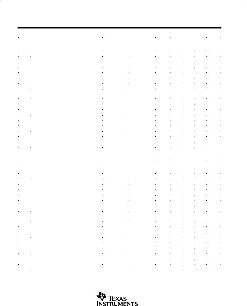
Percentage of Units ± %
DISTRIBUTION OF TLC279
INPUT OFFSET VOLTAGE
30
290 Units Tested From 2 Wafer Lots VDD = 5 V
25TA = 25°C
N Package
20
15
10
5
0 |
|
|
|
|
± 1200 |
± 600 |
0 |
600 |
1200 |
VIO ± Input Offset Voltage ± V
LinCMOS is a trademark of Texas Instruments Incorporated.
PRODUCTION DATA information is current as of publication date. Products conform to specifications per the terms of Texas Instruments standard warranty. Production processing does not necessarily include testing of all parameters.
Copyright 1998, Texas Instruments Incorporated
POST OFFICE BOX 655303 •DALLAS, TEXAS 75265 |
1 |

TLC274, TLC274A, TLC274B, TLC274Y, TLC279
LinCMOS PRECISION QUAD OPERATIONAL AMPLIFIERS
SLOS092C ± SEPTEMBER 1987 ± REVISED MARCH 1998
description (continued)
In general, many features associated with bipolar technology are available on LinCMOS operational amplifiers, without the power penalties of bipolar technology. General applications such as transducer interfacing, analog calculations, amplifier blocks, active filters, and signal buffering are easily designed with the TLC274 and TLC279. The devices also exhibit low voltage single-supply operation, making them ideally suited for remote and inaccessible battery-powered applications. The common-mode input voltage range includes the negative rail.
A wide range of packaging options is available, including small-outline and chip-carrier versions for high-density system applications.
The device inputs and outputs are designed to withstand ±100-mA surge currents without sustaining latch-up.
The TLC274 and TLC279 incorporate internal ESD-protection circuits that prevent functional failures at voltages up to 2000 V as tested under MIL-STD-883C, Method 3015.2; however, care should be exercised in handling these devices as exposure to ESD may result in the degradation of the device parametric performance.
The C-suffix devices are characterized for operation from 0°C to 70°C. The I-suffix devices are characterized for operation from ±40°C to 85°C. The M-suffix devices are characterized for operation over the full military temperature range of ±55°C to 125°C.
AVAILABLE OPTIONS
|
|
|
PACKAGED DEVICES |
|
CHIP |
|||
|
VIOmax |
|
|
|
|
|
||
|
SMALL |
CHIP |
CERAMIC |
PLASTIC |
|
|||
TA |
TSSOP |
FORM |
||||||
AT 25°C |
OUTLINE |
CARRIER |
DIP |
DIP |
||||
|
(PW) |
(Y) |
||||||
|
|
(D) |
(FK) |
(J) |
(N) |
|||
|
|
|
|
|||||
|
|
|
|
|
|
|
|
|
|
900 V |
TLC279CD |
Ð |
Ð |
TLC279CN |
Ð |
Ð |
|
0°C to 70°C |
2 mV |
TLC274BCD |
Ð |
Ð |
TLC274BCN |
Ð |
Ð |
|
5 mV |
TLC274ACD |
Ð |
Ð |
TLC274ACN |
Ð |
Ð |
||
|
||||||||
|
10 mV |
TLC274CD |
Ð |
Ð |
TLC274CN |
TLC274CPW |
TLC274Y |
|
|
|
|
|
|
|
|
|
|
|
900 V |
TLC279ID |
Ð |
Ð |
TLC279IN |
Ð |
Ð |
|
±40°C to 85°C |
2 mV |
TLC274BID |
Ð |
Ð |
TLC274BIN |
Ð |
Ð |
|
5 mV |
TLC274AID |
Ð |
Ð |
TLC274AIN |
Ð |
Ð |
||
|
||||||||
|
10 mV |
TLC274ID |
Ð |
Ð |
TLC274IN |
Ð |
Ð |
|
|
|
|
|
|
|
|
|
|
± 55°C to 125°C |
900 V |
TLC279MD |
TLC279MFK |
TLC279MJ |
TLC279MN |
Ð |
Ð |
|
10 mV |
TLC274MD |
TLC274MFK |
TLC274MJ |
TLC274MN |
Ð |
Ð |
||
|
||||||||
|
|
|
|
|
|
|
|
|
The D package is available taped and reeled. Add R suffix to the device type (e.g., TLC279CDR).
2 |
POST OFFICE BOX 655303 •DALLAS, TEXAS 75265 |
|
|
LinCMOS |
TLC274, TLC274A, TLC274B, TLC274Y, TLC279 |
||
|
|
PRECISION QUAD OPERATIONAL AMPLIFIERS |
|||
|
|
|
|
SLOS092C ± SEPTEMBER 1987 ± REVISED MARCH 1998 |
|
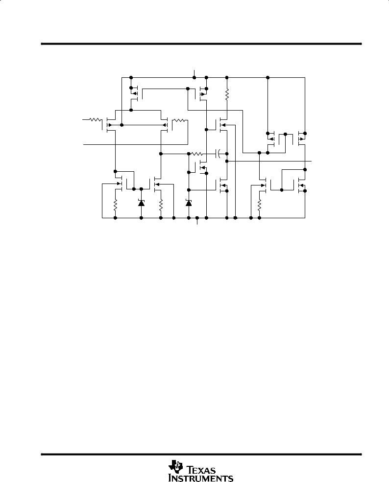
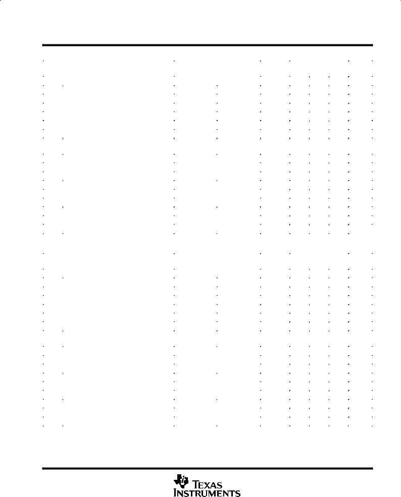
equivalent schematic (each amplifier) |
|
|
|
||
|
|
VDD |
|
|
|
P3 |
|
|
P4 |
|
|
|
|
|
|
R6 |
|
R1 |
|
R2 |
N5 |
|
|
IN ± |
|
|
|
|
|
|
|
|
|
P5 |
P6 |
P1 |
|
P2 |
|
|
|
IN + |
|
|
C1 |
|
|
|
|
|
R5 |
|
|
|
|
|
|
|
OUT |
|
|
|
N3 |
|
|
N1 |
N2 |
N4 |
N6 |
N7 |
|
R3 |
D1 |
R4 |
D2 |
R7 |
|
GND
POST OFFICE BOX 655303 •DALLAS, TEXAS 75265 |
3 |

TLC274, TLC274A, TLC274B, TLC274Y, TLC279
LinCMOS PRECISION QUAD OPERATIONAL AMPLIFIERS
SLOS092C ± SEPTEMBER 1987 ± REVISED MARCH 1998
TLC274Y chip information
These chips, when properly assembled, display characteristics similar to the TLC274C. Thermal compression or ultrasonic bonding may be used on the doped-aluminum bonding pads. Chips may be mounted with conductive epoxy or a gold-silicon preform.
|
BONDING PAD ASSIGNMENTS |
|
|
|
|
|
|||
|
|
|
|
|
|
|
VDD |
|
|
(14) |
(13) |
(12) |
(11) |
(10) |
(9) |
(8) |
(4) |
|
|
|
|
|
|
|
|
(3) |
+ |
|
|
|
|
|
|
|
|
1IN + |
(1) |
|
|
|
|
|
|
|
|
|
|
1OUT |
|
|
|
|
|
|
|
(2) |
|
|
|
|
|
|
|
|
|
1IN ± |
± |
|
|
|
|
|
|
|
|
|
+ |
(5) |
2IN + |
|
|
|
|
|
|
(7) |
|
||
|
|
|
|
|
|
|
|
||
|
|
|
|
|
|
2OUT |
± |
(6) |
2IN ± |
|
|
|
|
|
|
|
|||
68 |
|
|
|
|
|
(10) |
|
||
|
|
|
|
|
+ |
|
|
||
|
|
|
|
|
3IN + |
(8) |
|
||
|
|
|
|
|
|
3OUT |
|||
|
|
|
|
|
|
(9) |
|
|
|
|
|
|
|
|
|
3IN ± |
± |
|
|
|
|
|
|
|
|
(14) |
+ |
(12) |
4IN + |
|
|
|
|
|
|
4OUT |
± |
(13) |
4IN ± |
|
|
|
|
|
|
|
|||
(1) |
(2) |
(3) |
|
(5) |
(6) |
|
11 |
|
|
(4) |
(7) |
GND |
|
|
|||||
|
|
|
|
|
|
|
|
|
|
|
|
|
108 |
|
|
|
|
|
|
|
|
|
|
|
|
CHIP THICKNESS: 15 TYPICAL |
|
||
|
|
|
|
|
|
BONDING PADS: 4 × 4 MINIMUM |
|
||
|
|
|
|
|
|
TJmax = 150°C |
|
|
|
|
|
|
|
|
|
TOLERANCES ARE ± 10%. |
|
||
|
|
|
|
|
|
ALL DIMENSIONS ARE IN MILS. |
|
||
|
|
|
|
|
|
PIN (11) IS INTERNALLY CONNECTED |
|||
|
|
|
|
|
|
TO BACKSIDE OF CHIP. |
|
|
|
4 |
POST OFFICE BOX 655303 •DALLAS, TEXAS 75265 |
TLC274, TLC274A, TLC274B, TLC274Y, TLC279
LinCMOS PRECISION QUAD OPERATIONAL AMPLIFIERS
SLOS092C ± SEPTEMBER 1987 ± REVISED MARCH 1998
absolute maximum ratings over operating free-air temperature range (unless otherwise noted)²
Supply voltage, VDD (see Note 1) . . . . . . . . . . . . . . . . . . . . . . . . . . . . . . . . . . . . . . . |
. . . . . . . . . . . |
. . . . . . . . . . 18 V |
Differential input voltage, VID (see Note 2) . . . . . . . . . . . . . . . . . . . . . . . . . . . . . . . |
. . . . . . . . . . . . |
. . . . . . . . ± VDD |
Input voltage range, VI (any input) . . . . . . . . . . . . . . . . . . . . . . . . . . . . . . . . . . . . . . . |
. . . . . . . . . . . . |
±0.3 V to VDD |
Input current, II . . . . . . . . . . . . . . . . . . . . . . . . . . . . . . . . . . . . . . . . . . . . . . . . . . . . . . . |
. . . . . . . . . . . . |
. . . . . . . ± 5 mA |
Output current, lO (each output) . . . . . . . . . . . . . . . . . . . . . . . . . . . . . . . . . . . . . . . . |
. . . . . . . . . . . . |
. . . . . . ± 30 mA |
Total current into VDD . . . . . . . . . . . . . . . . . . . . . . . . . . . . . . . . . . . . . . . . . . . . . . . . . |
. . . . . . . . . . . . |
. . . . . . . 45 mA |
Total current out of GND . . . . . . . . . . . . . . . . . . . . . . . . . . . . . . . . . . . . . . . . . . . . . . . |
. . . . . . . . . . . . |
. . . . . . . 45 mA |
Duration of short-circuit current at (or below) 25°C (see Note 3) . . . . . . . . . . . . . |
. . . . . . . . . . . . |
. . . . . unlimited |
Continuous total dissipation . . . . . . . . . . . . . . . . . . . . . . . . . . . . . . . . . . . . . . . . . . . |
See Dissipation Rating Table |
|
Operating free-air temperature, TA: C suffix . . . . . . . . . . . . . . . . . . . . . . . . . . . . . . |
. . . . . . . . . . . . |
. . 0°C to 70°C |
I suffix . . . . . . . . . . . . . . . . . . . . . . . . . . . . . . . |
. . . . . . . . . . . . |
±40°C to 85°C |
M suffix . . . . . . . . . . . . . . . . . . . . . . . . . . . . . . |
. . . . . . . . . . . |
±55°C to 125°C |
Storage temperature range . . . . . . . . . . . . . . . . . . . . . . . . . . . . . . . . . . . . . . . . . . . . . |
. . . . . . . . . . . |
±65°C to 150°C |
Case temperature for 60 seconds: FK package . . . . . . . . . . . . . . . . . . . . . . . . . . . |
. . . . . . . . . . . . |
. . . . . . . 260°C |
Lead temperature 1,6 mm (1/16 inch) from case for 10 seconds: D, N, or PW package . . . . . |
. . . . . . . 260°C |
|
Lead temperature 1,6 mm (1/16 inch) from case for 60 seconds: J package . . |
. . . . . . . . . . . . |
. . . . . . . 300°C |
²Stresses beyond those listed under ªabsolute maximum ratingsº may cause permanent damage to the device. These are stress ratings only, and functional operation of the device at these or any other conditions beyond those indicated under ªrecommended operating conditionsº is not
implied. Exposure to absolute-maximum-rated conditions for extended periods may affect device reliability. NOTES: 1. All voltage values, except differential voltages, are with respect to network ground.
2.Differential voltages are at the noninverting input with respect to the inverting input.
3.The output may be shorted to either supply. Temperature and/or supply voltages must be limited to ensure that the maximum dissipation rating is not exceeded (see application section).
DISSIPATION RATING TABLE
PACKAGE |
TA ≤ 25°C |
DERATING FACTOR |
TA = 70°C |
TA = 85°C |
TA = 125°C |
|
POWER RATING |
ABOVE TA = 25°C |
POWER RATING |
POWER RATING |
POWER RATING |
||
|
||||||
D |
950 mW |
7.6 mW/°C |
608 mW |
494 mW |
Ð |
|
FK |
1375 mW |
11.0 mW/°C |
880 mW |
715 mW |
275 mW |
|
J |
1375 mW |
11.0 mW/°C |
880 mW |
715 mW |
275 mW |
|
N |
1575 mW |
12.6 mW/°C |
1008 mW |
819 mW |
Ð |
|
PW |
700 mW |
5.6 mW/°C |
448 mW |
Ð |
Ð |
|
|
|
|
|
|
|
recommended operating conditions
|
|
C SUFFIX |
I SUFFIX |
M SUFFIX |
UNIT |
||||
|
|
|
|
|
|
|
|
||
|
|
MIN |
MAX |
MIN |
MAX |
MIN |
MAX |
||
|
|
|
|||||||
|
|
|
|
|
|
|
|
|
|
Supply voltage, VDD |
|
3 |
16 |
4 |
16 |
4 |
16 |
V |
|
Common-mode input voltage, VIC |
VDD = 5 V |
± 0.2 |
3.5 |
± 0.2 |
3.5 |
0 |
3.5 |
V |
|
VDD = 10 V |
± 0.2 |
8.5 |
± 0.2 |
8.5 |
0 |
8.5 |
|||
|
|
||||||||
Operating free-air temperature, TA |
|
0 |
70 |
± 40 |
85 |
± 55 |
125 |
°C |
|
POST OFFICE BOX 655303 •DALLAS, TEXAS 75265 |
5 |
TLC274, TLC274A, TLC274B, TLC274Y, TLC279
LinCMOS PRECISION QUAD OPERATIONAL AMPLIFIERS
SLOS092C ± SEPTEMBER 1987 ± REVISED MARCH 1998
electrical characteristics at specified free-air temperature, VDD = 5 V (unless otherwise noted)
|
|
|
|
|
|
TLC274C, TLC274AC, |
|
||
|
PARAMETER |
TEST CONDITIONS |
T ² |
TLC274BC, TLC279C |
UNIT |
||||
|
|
|
|
|
A |
|
|
|
|
|
|
|
|
|
|
MIN |
TYP |
MAX |
|
|
|
|
|
|
|
|
|
|
|
|
|
TLC274C |
VO = 1.4 V, |
VIC = 0, |
25°C |
|
1.1 |
10 |
|
|
|
RS = 50 Ω, |
RL = 10 kΩ |
Full range |
|
|
12 |
mV |
|
|
|
|
|
|
|||||
|
|
TLC274AC |
VO = 1.4 V, |
VIC = 0, |
25°C |
|
0.9 |
5 |
|
|
|
|
|
||||||
VIO |
Input offset voltage |
RS = 50 Ω, |
RL = 10 kΩ |
Full range |
|
|
6.5 |
|
|
|
|
|
|
||||||
TLC274BC |
VO = 1.4 V, |
VIC = 0, |
25°C |
|
340 |
2000 |
|
||
|
|
|
|
||||||
|
|
RS = 50 Ω, |
RL = 10 kΩ |
Full range |
|
|
3000 |
µV |
|
|
|
|
|
|
|||||
|
|
TLC279C |
VO = 1.4 V, |
VIC = 0, |
25°C |
|
320 |
900 |
|
|
|
|
|
||||||
|
|
RS = 50 Ω, |
RL = 10 kΩ |
Full range |
|
|
1500 |
|
|
|
|
|
|
|
|
||||
αVIO |
Average temperature coefficient of input |
|
|
25°C to |
|
1.8 |
|
µV/°C |
|
offset voltage |
|
|
70°C |
|
|
||||
IIO |
Input offset current (see Note 4) |
VO = 2.5 V, |
VIC = 2.5 V |
25°C |
|
0.1 |
|
pA |
|
|
|
|
|
||||||
70°C |
|
7 |
300 |
||||||
|
|
|
|
|
|
|
|||
|
|
|
|
|
|
|
|
|
|
IIB |
Input bias current (see Note 4) |
VO = 2.5 V, |
VIC = 2.5 V |
25°C |
|
0.6 |
|
pA |
|
|
|
|
|
||||||
70°C |
|
40 |
600 |
||||||
|
|
|
|
|
|
|
|||
|
|
|
|
|
|
|
|
|
|
|
|
|
|
|
|
± 0.2 |
± 0.3 |
|
|
|
|
|
|
|
25°C |
to |
to |
|
V |
VICR |
Common-mode input voltage range |
|
|
|
4 |
4.2 |
|
|
|
(see Note 5) |
|
|
|
± 0.2 |
|
|
|
||
|
|
|
|
|
|
|
|||
|
|
|
|
|
Full range |
to |
|
|
V |
|
|
|
|
|
|
3.5 |
|
|
|
|
|
|
|
|
|
|
|
|
|
|
|
|
|
|
25°C |
3.2 |
3.8 |
|
|
|
|
|
RL = 10 kΩ |
|
|
|
|
|
|
VOH |
High-level output voltage |
VID = 100 mV, |
0°C |
3 |
3.8 |
|
V |
||
|
|
|
|
|
70°C |
3 |
3.8 |
|
|
|
|
|
|
|
|
|
|
|
|
|
|
|
|
|
25°C |
|
0 |
50 |
|
|
|
|
|
|
|
|
|
|
|
VOL |
Low-level output voltage |
VID = ± 100 mV, |
IOL = 0 |
0°C |
|
0 |
50 |
mV |
|
|
|
|
|
|
70°C |
|
0 |
50 |
|
|
|
|
|
|
|
|
|
|
|
|
Large-signal differential voltage |
|
|
25°C |
5 |
23 |
|
|
|
AVD |
VO = 0.25 V to 2 V, |
RL = 10 kΩ |
0°C |
4 |
27 |
|
V/mV |
||
amplification |
|
||||||||
|
|
|
70°C |
4 |
20 |
|
|
||
|
|
|
|
|
|
|
|||
|
|
|
|
|
25°C |
65 |
80 |
|
|
|
|
|
|
|
|
|
|
|
|
CMRR |
Common-mode rejection ratio |
VIC = VICRmin |
|
0°C |
60 |
84 |
|
dB |
|
|
|
|
|
|
70°C |
60 |
85 |
|
|
|
|
|
|
|
|
|
|
|
|
|
Supply-voltage rejection ratio |
|
|
25°C |
65 |
95 |
|
|
|
|
|
|
|
|
|
|
|
||
kSVR |
VDD = 5 V to 10 V, |
VO = 1.4 V |
0°C |
60 |
94 |
|
dB |
||
( VDD / VIO) |
|
||||||||
|
|
|
70°C |
60 |
96 |
|
|
||
|
|
|
|
|
|
|
|||
|
|
|
|
|
|
|
|
|
|
|
|
|
VO = 2.5 V, |
VIC = 2.5 V, |
25°C |
|
2.7 |
6.4 |
|
IDD |
Supply current (four amplifiers) |
0°C |
|
3.1 |
7.2 |
mA |
|||
No load |
|
|
|||||||
|
|
|
|
|
70°C |
|
2.3 |
5.2 |
|
|
|
|
|
|
|
|
|
|
|
² Full range is 0°C to 70°C.
NOTES: 4. The typical values of input bias current and input offset current below 5 pA were determined mathematically. 5. This range also applies to each input individually.
6 |
POST OFFICE BOX 655303 •DALLAS, TEXAS 75265 |
TLC274, TLC274A, TLC274B, TLC274Y, TLC279
LinCMOS PRECISION QUAD OPERATIONAL AMPLIFIERS
SLOS092C ± SEPTEMBER 1987 ± REVISED MARCH 1998
electrical characteristics at specified free-air temperature, VDD = 10 V (unless otherwise noted)
|
|
|
|
|
|
TLC274C, TLC274AC, |
|
||
|
PARAMETER |
TEST CONDITIONS |
T ² |
TLC274BC, TLC279C |
UNIT |
||||
|
|
|
|
|
A |
|
|
|
|
|
|
|
|
|
|
MIN |
TYP |
MAX |
|
|
|
|
|
|
|
|
|
|
|
|
|
TLC274C |
VO = 1.4 V, |
VIC = 0, |
25°C |
|
1.1 |
10 |
|
|
|
RS = 50 Ω, |
RL = 10 kΩ |
Full range |
|
|
12 |
mV |
|
|
|
|
|
|
|||||
|
|
TLC274AC |
VO = 1.4 V, |
VIC = 0, |
25°C |
|
0.9 |
5 |
|
|
|
|
|
||||||
VIO |
Input offset voltage |
RS = 50 Ω, |
RL = 10 kΩ |
Full range |
|
|
6.5 |
|
|
|
|
|
|
||||||
TLC274BC |
VO = 1.4 V, |
VIC = 0, |
25°C |
|
390 |
2000 |
|
||
|
|
|
|
||||||
|
|
RS = 50 Ω, |
RL = 10 kΩ |
Full range |
|
|
3000 |
µV |
|
|
|
|
|
|
|||||
|
|
TLC279C |
VO = 1.4 V, |
VIC = 0, |
25°C |
|
370 |
1200 |
|
|
|
|
|
||||||
|
|
RS = 50 Ω, |
RL = 10 kΩ |
Full range |
|
|
1900 |
|
|
|
|
|
|
|
|
||||
αVIO |
Average temperature coefficient of |
|
|
25°C to |
|
2 |
|
µV/°C |
|
input offset voltage |
|
|
70°C |
|
|
||||
IIO |
Input offset current (see Note 4) |
VO =.5 V, |
VIC = 5 V |
25°C |
|
0.1 |
|
pA |
|
|
|
|
|
||||||
70°C |
|
7 |
300 |
||||||
|
|
|
|
|
|
|
|||
|
|
|
|
|
|
|
|
|
|
IIB |
Input bias current (see Note 4) |
VO = 5 V, |
VIC = 5 V |
25°C |
|
0.7 |
|
pA |
|
|
|
|
|
||||||
70°C |
|
50 |
600 |
||||||
|
|
|
|
|
|
|
|||
|
|
|
|
|
|
|
|
|
|
|
|
|
|
|
|
± 0.2 |
± 0.3 |
|
|
|
|
|
|
|
25°C |
to |
to |
|
V |
VICR |
Common-mode input voltage range |
|
|
|
9 |
9.2 |
|
|
|
(see Note 5) |
|
|
|
± 0.2 |
|
|
|
||
|
|
|
|
|
|
|
|||
|
|
|
|
|
Full range |
to |
|
|
V |
|
|
|
|
|
|
8.5 |
|
|
|
|
|
|
|
|
|
|
|
|
|
|
|
|
|
|
25°C |
8 |
8.5 |
|
|
|
|
|
RL = 10 kΩ |
|
|
|
|
|
|
VOH |
High-level output voltage |
VID = 100 mV, |
0°C |
7.8 |
8.5 |
|
V |
||
|
|
|
|
|
70°C |
7.8 |
8.4 |
|
|
|
|
|
|
|
|
|
|
|
|
|
|
|
|
|
25°C |
|
0 |
50 |
|
|
|
|
|
|
|
|
|
|
|
VOL |
Low-level output voltage |
VID = ± 100 mV, |
IOL = 0 |
0°C |
|
0 |
50 |
mV |
|
|
|
|
|
|
70°C |
|
0 |
50 |
|
|
|
|
|
|
|
|
|
|
|
|
Large-signal differential voltage |
|
|
25°C |
10 |
36 |
|
|
|
AVD |
VO = 1 V to 6 V, |
RL = 10 kΩ |
0°C |
7.5 |
42 |
|
V/mV |
||
amplification |
|
||||||||
|
|
|
70°C |
7.5 |
32 |
|
|
||
|
|
|
|
|
|
|
|||
|
|
|
|
|
25°C |
65 |
85 |
|
|
|
|
|
|
|
|
|
|
|
|
CMRR |
Common-mode rejection ratio |
VIC = VICRmin |
|
0°C |
60 |
88 |
|
dB |
|
|
|
|
|
|
70°C |
60 |
88 |
|
|
|
|
|
|
|
|
|
|
|
|
|
Supply-voltage rejection ratio |
|
|
25°C |
65 |
95 |
|
|
|
|
|
|
|
|
|
|
|
||
kSVR |
VDD = 5 V to 10 V, |
VO = 1.4 V |
0°C |
60 |
94 |
|
dB |
||
( VDD / VIO) |
|
||||||||
|
|
|
70°C |
60 |
96 |
|
|
||
|
|
|
|
|
|
|
|||
|
|
|
|
|
|
|
|
|
|
|
|
|
VO = 5 V, |
VIC = 5 V, |
25°C |
|
3.8 |
8 |
|
IDD |
Supply current (four amplifiers) |
0°C |
|
4.5 |
8.8 |
mA |
|||
No load |
|
|
|||||||
|
|
|
|
|
70°C |
|
3.2 |
6.8 |
|
|
|
|
|
|
|
|
|
|
|
² Full range is 0°C to 70°C.
NOTES: 4. The typical values of input bias current and input offset current below 5 pA were determined mathematically. 5. This range also applies to each input individually.
POST OFFICE BOX 655303 •DALLAS, TEXAS 75265 |
7 |
TLC274, TLC274A, TLC274B, TLC274Y, TLC279
LinCMOS PRECISION QUAD OPERATIONAL AMPLIFIERS
SLOS092C ± SEPTEMBER 1987 ± REVISED MARCH 1998
electrical characteristics at specified free-air temperature, VDD = 5 V (unless otherwise noted)
|
|
|
|
|
|
TLC274I, TLC274AI, |
|
||
|
PARAMETER |
TEST CONDITIONS |
T ² |
TLC274BI, TLC279I |
UNIT |
||||
|
|
|
|
|
A |
|
|
|
|
|
|
|
|
|
|
MIN |
TYP |
MAX |
|
|
|
|
|
|
|
|
|
|
|
|
|
TLC274I |
VO = 1.4 V, |
VIC = 0, |
25°C |
|
1.1 |
10 |
|
|
|
RS = 50 Ω, |
RL = 10 kΩ |
Full range |
|
|
13 |
mV |
|
|
|
|
|
|
|||||
|
|
TLC274AI |
VO = 1.4 V, |
VIC = 0, |
25°C |
|
0.9 |
5 |
|
|
|
|
|
||||||
VIO |
Input offset voltage |
RS = 50 Ω, |
RL = 10 kΩ |
Full range |
|
|
7 |
|
|
|
|
|
|
||||||
TLC274BI |
VO = 1.4 V, |
VIC = 0, |
25°C |
|
340 |
2000 |
|
||
|
|
|
|
||||||
|
|
RS = 50 Ω, |
RL = 10 kΩ |
Full range |
|
|
3500 |
µV |
|
|
|
|
|
|
|||||
|
|
TLC279I |
VO = 1.4 V, |
VIC = 0, |
25°C |
|
320 |
900 |
|
|
|
|
|
||||||
|
|
RS = 50 Ω, |
RL = 10 kΩ |
Full range |
|
|
2000 |
|
|
|
|
|
|
|
|
||||
αVIO |
Average temperature coefficient of input |
|
|
25°C to |
|
1.8 |
|
µV/°C |
|
offset voltage |
|
|
85°C |
|
|
||||
IIO |
Input offset current (see Note 4) |
VO = 2.5 V, |
VIC = 2.5 V |
25°C |
|
0.1 |
|
pA |
|
|
|
|
|
||||||
85°C |
|
24 |
1000 |
||||||
|
|
|
|
|
|
|
|||
|
|
|
|
|
|
|
|
|
|
IIB |
Input bias current (see Note 4) |
VO = 2.5 V, |
VIC = 2.5 V |
25°C |
|
0.6 |
|
pA |
|
|
|
|
|
||||||
85°C |
|
200 |
2000 |
||||||
|
|
|
|
|
|
|
|||
|
|
|
|
|
|
|
|
|
|
|
|
|
|
|
25°C |
± 0.2 |
± 0.3 |
|
|
|
|
|
|
|
to |
to |
|
V |
|
VICR |
Common-mode input voltage range |
|
|
|
4 |
4.2 |
|
|
|
(see Note 5) |
|
|
Full range |
± 0.2 |
|
|
V |
||
|
|
|
|
|
to |
|
|
||
|
|
|
|
|
|
3.5 |
|
|
|
|
|
|
|
|
|
|
|
|
|
|
|
|
|
|
25°C |
3.2 |
3.8 |
|
|
|
|
|
RL = 10 kΩ |
|
|
|
|
|
|
VOH |
High-level output voltage |
VID = 100 mV, |
± 40°C |
3 |
3.8 |
|
V |
||
|
|
|
|
|
85°C |
3 |
3.8 |
|
|
|
|
|
|
|
|
|
|
|
|
|
|
|
|
|
25°C |
|
0 |
50 |
|
|
|
|
|
|
|
|
|
|
|
VOL |
Low-level output voltage |
VID = ±100 mV, |
IOL = 0 |
± 40°C |
|
0 |
50 |
mV |
|
|
|
|
|
|
85°C |
|
0 |
50 |
|
|
|
|
|
|
|
|
|
|
|
|
Large-signal differential voltage |
|
|
25°C |
5 |
23 |
|
|
|
AVD |
VO = 0.25 V to 2 V, |
RL = 10 kΩ |
± 40°C |
3.5 |
32 |
|
V/mV |
||
amplification |
|
||||||||
|
|
|
85°C |
3.5 |
19 |
|
|
||
|
|
|
|
|
|
|
|||
|
|
|
|
|
25°C |
65 |
80 |
|
|
|
|
|
|
|
|
|
|
|
|
CMRR |
Common-mode rejection ratio |
VIC = VICRmin |
|
± 40°C |
60 |
81 |
|
dB |
|
|
|
|
|
|
85°C |
60 |
86 |
|
|
|
|
|
|
|
|
|
|
|
|
|
Supply-voltage rejection ratio |
|
|
25°C |
65 |
95 |
|
|
|
|
|
|
|
|
|
|
|
||
kSVR |
VDD = 5 V to 10 V, |
VO = 1.4 V |
± 40°C |
60 |
92 |
|
dB |
||
( VDD / VIO) |
|
||||||||
|
|
|
85°C |
60 |
96 |
|
|
||
|
|
|
|
|
|
|
|||
|
|
|
|
|
|
|
|
|
|
|
|
|
VO = 2.5 V, |
VIC = 2.5 V, |
25°C |
|
2.7 |
6.4 |
|
IDD |
Supply current (four amplifiers) |
± 40°C |
|
3.8 |
8.8 |
mA |
|||
No load |
|
|
|||||||
|
|
|
|
|
85°C |
|
2.1 |
4.8 |
|
|
|
|
|
|
|
|
|
|
|
² Full range is ± 40°C to 85°C.
NOTES: 4. The typical values of input bias current and input offset current below 5 pA were determined mathematically. 5. This range also applies to each input individually.
8 |
POST OFFICE BOX 655303 •DALLAS, TEXAS 75265 |
TLC274, TLC274A, TLC274B, TLC274Y, TLC279
LinCMOS PRECISION QUAD OPERATIONAL AMPLIFIERS
SLOS092C ± SEPTEMBER 1987 ± REVISED MARCH 1998
electrical characteristics at specified free-air temperature, VDD = 10 V (unless otherwise noted)
|
|
|
|
|
|
TLC274I, TLC274AI, |
|
||
|
PARAMETER |
TEST CONDITIONS |
T ² |
TLC274BI, TLC279I |
UNIT |
||||
|
|
|
|
|
A |
|
|
|
|
|
|
|
|
|
|
MIN |
TYP |
MAX |
|
|
|
|
|
|
|
|
|
|
|
|
|
TLC274I |
VO = 1.4 V, |
VIC = 0, |
25°C |
|
1.1 |
10 |
|
|
|
RS = 50 Ω, |
RL = 10 kΩ |
Full range |
|
|
13 |
mV |
|
|
|
|
|
|
|||||
|
|
TLC274AI |
VO = 1.4 V, |
VIC = 0, |
25°C |
|
0.9 |
5 |
|
|
|
|
|
||||||
VIO |
Input offset voltage |
RS = 50 Ω, |
RL = 10 kΩ |
Full range |
|
|
7 |
|
|
|
|
|
|
||||||
TLC274BI |
VO = 1.4 V, |
VIC = 0, |
25°C |
|
390 |
2000 |
|
||
|
|
|
|
||||||
|
|
RS = 50 Ω, |
RL = 10 kΩ |
Full range |
|
|
3500 |
µV |
|
|
|
|
|
|
|||||
|
|
TLC279I |
VO = 1.4 V, |
VIC = 0, |
25°C |
|
370 |
1200 |
|
|
|
|
|
||||||
|
|
RS = 50 Ω, |
RL = 10 kΩ |
Full range |
|
|
2900 |
|
|
|
|
|
|
|
|
||||
αVIO |
Average temperature coefficient of input |
|
|
25°C to |
|
2 |
|
µV/°C |
|
offset voltage |
|
|
85°C |
|
|
||||
IIO |
Input offset current (see Note 4) |
VO = 5 V, |
VIC = 5 V |
25°C |
|
0.1 |
|
pA |
|
|
|
|
|
||||||
85°C |
|
26 |
1000 |
||||||
|
|
|
|
|
|
|
|||
|
|
|
|
|
|
|
|
|
|
IIB |
Input bias current (see Note 4) |
VO = 5 V, |
VIC = 5 V |
25°C |
|
0.7 |
|
pA |
|
|
|
|
|
||||||
85°C |
|
220 |
2000 |
||||||
|
|
|
|
|
|
|
|||
|
|
|
|
|
|
|
|
|
|
|
|
|
|
|
|
± 0.2 |
± 0.3 |
|
|
|
|
|
|
|
25°C |
to |
to |
|
V |
VICR |
Common-mode input voltage range |
|
|
|
9 |
9.2 |
|
|
|
(see Note 5) |
|
|
|
± 0.2 |
|
|
|
||
|
|
|
|
|
|
|
|||
|
|
|
|
|
Full range |
to |
|
|
V |
|
|
|
|
|
|
8.5 |
|
|
|
|
|
|
|
|
|
|
|
|
|
|
|
|
|
|
25°C |
8 |
8.5 |
|
|
|
|
|
RL = 10 kΩ |
|
|
|
|
|
|
VOH |
High-level output voltage |
VID = 100 mV, |
± 40°C |
7.8 |
8.5 |
|
V |
||
|
|
|
|
|
85°C |
7.8 |
8.5 |
|
|
|
|
|
|
|
|
|
|
|
|
|
|
|
|
|
25°C |
|
0 |
50 |
|
|
|
|
|
|
|
|
|
|
|
VOL |
Low-level output voltage |
VID = ± 100 mV, |
IOL = 0 |
± 40°C |
|
0 |
50 |
mV |
|
|
|
|
|
|
85°C |
|
0 |
50 |
|
|
|
|
|
|
|
|
|
|
|
|
Large-signal differential voltage |
|
|
25°C |
10 |
36 |
|
|
|
AVD |
VO = 1 V to 6 V, |
RL = 10 kΩ |
± 40°C |
7 |
47 |
|
V/mV |
||
amplification |
|
||||||||
|
|
|
85°C |
7 |
31 |
|
|
||
|
|
|
|
|
|
|
|||
|
|
|
|
|
25°C |
65 |
85 |
|
|
|
|
|
|
|
|
|
|
|
|
CMRR |
Common-mode rejection ratio |
VIC = VICRmin |
|
± 40°C |
60 |
87 |
|
dB |
|
|
|
|
|
|
85°C |
60 |
88 |
|
|
|
|
|
|
|
|
|
|
|
|
|
Supply-voltage rejection ratio |
|
|
25°C |
65 |
95 |
|
|
|
|
|
|
|
|
|
|
|
||
kSVR |
VDD = 5 V to 10 V, |
VO = 1.4 V |
± 40°C |
60 |
92 |
|
dB |
||
( VDD / VIO) |
|
||||||||
|
|
|
85°C |
60 |
96 |
|
|
||
|
|
|
|
|
|
|
|||
|
|
|
|
|
|
|
|
|
|
|
|
|
VO = 5 V, |
VIC = 5 V, |
25°C |
|
3.8 |
8 |
|
IDD |
Supply current (four amplifiers) |
± 40°C |
|
5.5 |
10 |
mA |
|||
No load |
|
|
|||||||
|
|
|
|
|
85°C |
|
2.9 |
6.4 |
|
|
|
|
|
|
|
|
|
|
|
² Full range is ± 40°C to 85°C. |
|
|
|
|
|
|
|
||
NOTES: |
4. The typical values of input bias current and input offset current below 5 pA were determined mathematically. |
|
|
||||||
|
5. This range also applies to each input individually. |
|
|
|
|
|
|
||
POST OFFICE BOX 655303 •DALLAS, TEXAS 75265 |
9 |

TLC274, TLC274A, TLC274B, TLC274Y, TLC279
LinCMOS PRECISION QUAD OPERATIONAL AMPLIFIERS
SLOS092C ± SEPTEMBER 1987 ± REVISED MARCH 1998
electrical characteristics at specified free-air temperature, VDD = 5 V (unless otherwise noted)
|
PARAMETER |
TEST CONDITIONS |
T ² |
TLC274M, TLC279M |
UNIT |
||||
|
|
|
|
||||||
|
|
|
|
||||||
|
|
|
|
|
A |
MIN |
TYP |
MAX |
|
|
|
|
|
|
|
|
|||
|
|
TLC274M |
VO = 1.4 V, |
VIC = 0, |
25°C |
|
1.1 |
10 |
mV |
VIO |
Input offset voltage |
RS = 50 Ω, |
RL = 10 kΩ |
Full range |
|
|
12 |
||
|
|
|
|
||||||
TLC279M |
VO = 1.4 V, |
VIC = 0, |
25°C |
|
320 |
900 |
µV |
||
|
|
|
|||||||
|
|
|
|
|
|
||||
|
|
Full range |
|
|
3750 |
||||
|
|
|
RS = 50 Ω, |
RL = 10 kΩ |
|
|
|
||
αVIO |
Average temperature coefficient of input |
|
|
25°C to |
|
2.1 |
|
µV/°C |
|
offset voltage |
|
|
125°C |
|
|
||||
IIO |
Input offset current (see Note 4) |
VO = 2.5 V, |
VIC = 2.5 V |
25°C |
|
0.1 |
|
pA |
|
|
|
|
|
|
|||||
125°C |
|
1.4 |
15 |
nA |
|||||
|
|
|
|
|
|
||||
|
|
|
|
|
|
|
|
|
|
IIB |
Input bias current (see Note 4) |
VO = 2.5 V, |
VIC = 2.5 V |
25°C |
|
0.6 |
|
pA |
|
|
|
|
|
|
|||||
125°C |
|
9 |
35 |
nA |
|||||
|
|
|
|
|
|
||||
|
|
|
|
|
25°C |
0 |
± 0.3 |
|
|
|
|
|
|
|
to |
to |
|
V |
|
VICR |
Common-mode input voltage range |
|
|
|
4 |
4.2 |
|
|
|
(see Note 5) |
|
|
|
0 |
|
|
|
||
|
|
|
|
|
Full range |
to |
|
|
V |
|
|
|
|
|
|
3.5 |
|
|
|
|
|
|
|
|
|
|
|
|
|
|
|
|
|
|
25°C |
3.2 |
3.8 |
|
|
|
|
|
RL = 10 kΩ |
|
|
|
|
|
|
VOH |
High-level output voltage |
VID = 100 mV, |
± 55°C |
3 |
3.8 |
|
V |
||
|
|
|
|
|
125°C |
3 |
3.8 |
|
|
|
|
|
|
|
|
|
|
|
|
|
|
|
|
|
25°C |
|
0 |
50 |
|
|
|
|
|
|
|
|
|
|
|
VOL |
Low-level output voltage |
VID = ± 100 mV, |
IOL = 0 |
± 55°C |
|
0 |
50 |
mV |
|
|
|
|
|
|
125°C |
|
0 |
50 |
|
|
Large-signal differential voltage |
|
|
25°C |
5 |
23 |
|
|
|
|
|
RL = 10 kΩ |
|
|
|
|
|
||
AVD |
VO = 0.25 V to 2 V, |
± 55°C |
3.5 |
35 |
|
V/mV |
|||
amplification |
|
||||||||
|
|
|
125°C |
3.5 |
16 |
|
|
||
|
|
|
|
|
|
|
|||
|
|
|
|
|
|
|
|
|
|
|
|
|
|
|
25°C |
65 |
80 |
|
|
CMRR |
Common-mode rejection ratio |
VIC = VICRmin |
|
± 55°C |
60 |
81 |
|
dB |
|
|
|
|
|
|
125°C |
60 |
84 |
|
|
|
|
|
|
|
|
|
|
|
|
|
Supply-voltage rejection ratio |
|
|
25°C |
65 |
95 |
|
|
|
|
|
|
|
|
|
|
|
||
kSVR |
VDD = 5 V to 10 V, |
VO = 1.4 V |
± 55°C |
60 |
90 |
|
dB |
||
( VDD / VIO) |
|
||||||||
|
|
|
125°C |
60 |
97 |
|
|
||
|
|
|
|
|
|
|
|||
|
|
|
VO = 2.5 V, |
VIC = 2.5 V, |
25°C |
|
2.7 |
6.4 |
|
|
|
|
|
|
|
|
|
||
IDD |
Supply current (four amplifiers) |
± 55°C |
|
4 |
10 |
mA |
|||
No load |
|
|
|||||||
|
|
|
|
|
125°C |
|
1.9 |
4.4 |
|
|
|
|
|
|
|
|
|
|
|
² Full range is ± 55°C to 125°C. |
|
|
|
|
|
|
|
||
NOTES: |
4. The typical values of input bias current and input offset current below 5 pA were determined mathematically. |
|
|
||||||
|
5. This range also applies to each input individually. |
|
|
|
|
|
|
||
10 |
POST OFFICE BOX 655303 •DALLAS, TEXAS 75265 |
TLC274, TLC274A, TLC274B, TLC274Y, TLC279
LinCMOS PRECISION QUAD OPERATIONAL AMPLIFIERS
SLOS092C ± SEPTEMBER 1987 ± REVISED MARCH 1998
electrical characteristics at specified free-air temperature, VDD = 10 V (unless) otherwise noted)
|
PARAMETER |
TEST CONDITIONS |
T ² |
TLC274M, TLC279M |
UNIT |
||||
|
|
|
|
||||||
|
|
|
|
||||||
|
|
|
|
|
A |
MIN |
TYP |
MAX |
|
|
|
|
|
|
|
|
|||
|
|
TLC274M |
VO = 1.4 V, |
VIC = 0, |
25°C |
|
1.1 |
10 |
mV |
VIO |
Input offset voltage |
RS = 50 Ω, |
RL = 10 kΩ |
Full range |
|
|
12 |
||
|
|
|
|
||||||
TLC279M |
VO = 1.4 V, |
VIC = 0, |
25°C |
|
370 |
1200 |
µV |
||
|
|
|
|||||||
|
|
|
|
|
|
||||
|
|
Full range |
|
|
4300 |
||||
|
|
|
RS = 50 Ω, |
RL = 10 kΩ |
|
|
|
||
αVIO |
Average temperature coefficient of input |
|
|
25°C to |
|
2.2 |
|
µV/°C |
|
offset voltage |
|
|
125°C |
|
|
||||
IIO |
Input offset current (see Note 4) |
VO = 5 V, |
VIC = 5 V |
25°C |
|
0.1 |
|
pA |
|
|
|
|
|
|
|||||
125°C |
|
1.8 |
15 |
nA |
|||||
|
|
|
|
|
|
||||
IIB |
Input bias current (see Note 4) |
VO = 5 V, |
VIC = 5 V |
25°C |
|
0.7 |
|
pA |
|
|
|
|
|
|
|||||
125°C |
|
10 |
35 |
nA |
|||||
|
|
|
|
|
|
||||
|
|
|
|
|
25°C |
0 |
± 0.3 |
|
V |
|
|
|
|
|
to |
to |
|
||
VICR |
Common-mode input voltage range |
|
|
|
9 |
9.2 |
|
|
|
(see Note 5) |
|
|
|
0 |
|
|
|
||
|
|
|
|
|
Full range |
to |
|
|
V |
|
|
|
|
|
|
8.5 |
|
|
|
|
|
|
|
|
25°C |
8 |
8.5 |
|
|
|
|
|
RL = 10 kΩ |
|
|
|
|
|
|
VOH |
High-level output voltage |
VID = 100 mV, |
± 55°C |
7.8 |
8.5 |
|
V |
||
|
|
|
|
|
125°C |
7.8 |
8.4 |
|
|
|
|
|
|
|
|
|
|
|
|
|
|
|
|
|
25°C |
|
0 |
50 |
|
VOL |
Low-level output voltage |
VID = ± 100 mV, |
IOL = 0 |
± 55°C |
|
0 |
50 |
mV |
|
|
|
|
|
|
125°C |
|
0 |
50 |
|
|
|
|
|
|
|
|
|
|
|
|
Large-signal differential voltage |
|
|
25°C |
10 |
36 |
|
|
|
|
|
RL = 10 kΩ |
|
|
|
|
|
||
AVD |
VO = 1 V to 6 V, |
± 55°C |
7 |
50 |
|
V/mV |
|||
amplification |
|
||||||||
|
|
|
125°C |
7 |
27 |
|
|
||
|
|
|
|
|
|
|
|||
|
|
|
|
|
25°C |
65 |
85 |
|
|
|
|
|
|
|
|
|
|
|
|
CMRR |
Common-mode rejection ratio |
VIC = VICRmin |
|
± 55°C |
60 |
87 |
|
dB |
|
|
|
|
|
|
125°C |
60 |
86 |
|
|
|
|
|
|
|
|
|
|
|
|
|
Supply-voltage rejection ratio |
|
|
25°C |
65 |
95 |
|
|
|
kSVR |
VDD = 5 V to 10 V, |
VO = 1.4 V |
± 55°C |
60 |
90 |
|
dB |
||
( VDD / VIO) |
|
||||||||
|
|
|
125°C |
60 |
97 |
|
|
||
|
|
|
|
|
|
|
|||
|
|
|
VO = 5 V, |
VIC = 5 V, |
25°C |
|
3.8 |
8 |
|
|
|
|
|
|
|
|
|
||
IDD |
Supply current (four amplifiers) |
± 55°C |
|
6.0 |
12 |
mA |
|||
No load |
|
|
|||||||
|
|
|
|
|
125°C |
|
2.5 |
5.6 |
|
² Full range is ± 55°C to 125°C. |
|
|
|
|
|
|
|
||
NOTES: |
4. The typical values of input bias current and input offset current below 5 pA were determined mathematically. |
|
|
||||||
|
5. This range also applies to each input individually. |
|
|
|
|
|
|
||
POST OFFICE BOX 655303 •DALLAS, TEXAS 75265 |
11 |
TLC274, TLC274A, TLC274B, TLC274Y, TLC279
LinCMOS PRECISION QUAD OPERATIONAL AMPLIFIERS
SLOS092C ± SEPTEMBER 1987 ± REVISED MARCH 1998
operating characteristics at specified free-air temperature, VDD = 5 V
|
|
|
|
|
TLC274C, TLC274AC, |
|
|
|
|
|
PARAMETER |
TEST CONDITIONS |
TA |
TLC274AC, |
UNIT |
||||
|
TLC274BC, TLC279C |
||||||||
|
|
|
|
|
|
|
|
|
|
|
|
|
|
|
MIN TYP MAX |
|
|
|
|
|
|
|
|
|
|
|
|
|
|
|
|
|
|
25°C |
3.6 |
|
|
|
|
|
|
|
|
|
|
|
|
|
|
|
|
RL = 10 Ω, |
VIPP = 1 V |
0°C |
4 |
|
|
|
|
SR |
Slew rate at unity gain |
|
70°C |
3 |
V/µs |
||||
CL = 20 PF, |
|
|
|
||||||
|
25°C |
2.9 |
|||||||
|
|
See Figure 1 |
|
|
|
|
|||
|
|
|
VIPP = 2.5 V |
0°C |
3.1 |
|
|
|
|
|
|
|
|
70°C |
2.5 |
|
|
|
|
|
|
f = 1 kHz, |
RS = 20 Ω , |
25°C |
|
|
|
|
|
Vn |
Equivalent input noise voltage |
25 |
nV/√ Hz |
||||||
See Figure 2 |
|||||||||
|
|
|
|
|
|
|
|
||
|
|
|
|
|
|
|
|
|
|
|
|
VO = VOH, |
CL = 20 PF, |
25°C |
320 |
|
|
|
|
|
|
|
|
|
|
|
|||
BOM |
Maximum output-swing bandwidth |
0°C |
340 |
kHz |
|||||
RL = 10 kΩ, |
See Figure 1 |
||||||||
|
|
70°C |
260 |
|
|
|
|||
|
|
|
|
|
|
|
|||
|
|
|
|
|
|
|
|
|
|
|
|
VI = 10 mV, |
CL = 20 PF, |
25°C |
1.7 |
|
|
|
|
|
|
|
|
|
|
|
|||
B1 |
Unity-gain bandwidth |
0°C |
2 |
MHz |
|||||
See Figure 3 |
|
||||||||
|
|
|
|
70°C |
1.3 |
|
|
|
|
|
|
VI = 10 mV, |
f = B1, |
25°C |
46° |
|
|
|
|
φm |
|
|
|
|
|
|
|||
Phase margin |
0°C |
47° |
|
|
|
||||
|
|
CL = 20 PF, |
|
|
|
|
|
|
|
|
|
|
70°C |
44° |
|
|
|
||
|
|
|
|
|
|
|
|||
|
|
|
|
|
|
|
|
|
|
operating characteristics at specified free-air temperature, VDD = 10 V
|
|
|
|
|
TLC274C, TLC274AC, |
|
|
|
|
|
PARAMETER |
TEST CONDITIONS |
TA |
TLC274AC, |
UNIT |
|
|||
|
TLC274BC, TLC279C |
|
|||||||
|
|
|
|
|
|
|
|
|
|
|
|
|
|
|
MIN TYP MAX |
|
|
|
|
|
|
|
|
|
|
|
|
|
|
|
|
|
|
25°C |
5.3 |
|
|
|
|
|
|
|
|
|
|
|
|
|
|
|
|
RL = 10 Ω, |
VIPP = 1 V |
0°C |
5.9 |
|
|
|
|
SR |
Slew rate at unity gain |
|
70°C |
4.3 |
V/µs |
|
|||
CL = 20 PF, |
|
|
|
|
|||||
|
25°C |
4.6 |
|
||||||
|
|
See Figure 1 |
|
|
|
|
|
||
|
|
|
VIPP = 5.5 V |
0°C |
5.1 |
|
|
|
|
|
|
|
|
70°C |
3.8 |
|
|
|
|
|
|
f = 1 kHz, |
RS = 20 Ω, |
25°C |
|
|
|
|
|
Vn |
Equivalent input noise voltage |
25 |
nV/√ Hz |
|
|||||
See Figure 2 |
|
||||||||
|
|
|
|
|
|
|
|
|
|
|
|
|
|
|
|
|
|
|
|
|
|
VO = VOH, |
CL = 20 PF, |
25°C |
200 |
|
|
|
|
|
|
|
|
|
|
|
|
||
BOM |
Maximum output-swing bandwidth |
0°C |
220 |
kHz |
|
||||
RL = 10 kΩ, |
See Figure 1 |
|
|||||||
|
|
70°C |
140 |
|
|
|
|
||
|
|
|
|
|
|
|
|
||
|
|
|
|
|
|
|
|
|
|
|
|
VI = 10 mV, |
CL = 20 PF, |
25°C |
2.2 |
|
|
|
|
|
|
|
|
|
|
|
|
||
B1 |
Unity-gain bandwidth |
0°C |
2.5 |
MHz |
|
||||
See Figure 3 |
|
|
|||||||
|
|
|
|
70°C |
1.8 |
|
|
|
|
|
|
VI = 10 mV, |
f = B1, |
25°C |
49° |
|
|
|
|
φm |
|
|
|
|
|
|
|
||
Phase margin |
0°C |
50° |
|
|
|
|
|||
|
|
CL = 20 PF, |
See Figure 3 |
|
|
|
|
|
|
|
|
70°C |
46° |
|
|
|
|
||
|
|
|
|
|
|
|
|
||
|
|
|
|
|
|
|
|
|
|
|
|
|
|
|
|
|
|
|
|
|
|
|
|
|
|
|
|
|
|
12 |
POST OFFICE BOX 655303 •DALLAS, TEXAS 75265 |
TLC274, TLC274A, TLC274B, TLC274Y, TLC279
LinCMOS PRECISION QUAD OPERATIONAL AMPLIFIERS
SLOS092C ± SEPTEMBER 1987 ± REVISED MARCH 1998
operating characteristics at specified free-air temperature, VDD = 5 V
|
|
|
|
|
|
TLC274I, TLC274AI, |
|
|
|
|
|
PARAMETER |
|
TEST CONDITIONS |
TA |
TLC274BI, TLC279I |
UNIT |
||||
|
|
|
|
|
|
MIN TYP MAX |
|
|
|
|
|
|
|
|
|
|
|
|
|
|
|
|
|
|
|
|
25°C |
3.6 |
|
|
|
|
|
|
|
|
|
|
|
|
|
|
|
|
|
RL = 10 kΩ, |
VIPP = 1 V |
± 40°C |
4.5 |
|
|
|
||
SR |
Slew rate at unity gain |
|
85°C |
2.8 |
V/µs |
|||||
CL = 20 PF, |
|
|
|
|||||||
|
25°C |
2.9 |
||||||||
|
|
See Figure 1 |
|
|
|
|
||||
|
|
|
|
|
|
|
|
|||
|
|
|
|
VIPP = 2.5 V |
± 40°C |
3.5 |
|
|
|
|
|
|
|
|
|
85°C |
2.3 |
|
|
|
|
|
|
|
|
|
|
|
|
|
||
|
|
f = 1 kHz, |
RS = 20 Ω, |
25°C |
|
|
|
|
||
Vn |
Equivalent input noise voltage |
25 |
nV/√ Hz |
|||||||
See Figure 2 |
|
|||||||||
|
|
|
|
|
|
|
|
|||
|
|
|
|
|
|
|
|
|
|
|
|
|
VO = VOH, |
CL = 20 PF, |
25°C |
320 |
|
|
|
||
|
|
|
|
|
|
|
||||
BOM |
Maximum output-swing bandwidth |
± 40°C |
380 |
kHz |
||||||
RL |
= 10 kΩ, |
See Figure 1 |
||||||||
|
|
85°C |
250 |
|
|
|
||||
|
|
|
|
|
|
|
|
|||
|
|
|
|
|
|
|
|
|
|
|
|
|
VI = 10 mV, |
CL = 20 PF, |
25°C |
1.7 |
|
|
|
||
|
|
|
|
|
|
|
||||
B1 |
Unity-gain bandwidth |
± 40°C |
2.6 |
MHz |
||||||
See Figure 3 |
|
|||||||||
|
|
|
|
|
85°C |
1.2 |
|
|
|
|
|
|
|
|
|
|
|
|
|
|
|
|
|
VI = 10 mV, |
f = B1, |
25°C |
46° |
|
|
|
||
m |
Phase margin |
± 40°C |
49° |
|
|
|
||||
CL |
= 20 PF, |
See Figure 3 |
|
|
|
|||||
|
|
|
|
|
|
|
||||
|
|
85°C |
43° |
|
|
|
||||
|
|
|
|
|
|
|
|
|||
|
|
|
|
|
|
|
|
|
|
|
operating characteristics at specified free-air temperature, VDD = 10 V
|
|
|
|
|
|
TLC274I, TLC274AI, |
|
|
|
|
|
PARAMETER |
|
TEST CONDITIONS |
TA |
TLC274BI, TLC279I |
UNIT |
||||
|
|
|
|
|
|
MIN TYP MAX |
|
|
|
|
|
|
|
|
|
|
|
|
|
|
|
|
|
|
|
|
25°C |
5.3 |
|
|
|
|
|
|
RL = 10 Ω, |
VIPP = 1 V |
± 40°C |
6.7 |
|
|
|
||
SR |
Slew rate at unity gain |
|
85°C |
4 |
V/µs |
|||||
CL = 20 PF, |
|
|
|
|||||||
|
25°C |
4.6 |
||||||||
|
|
See Figure 1 |
|
|
|
|
||||
|
|
|
|
|
|
|
|
|||
|
|
|
|
VIPP = 5.5 V |
± 40°C |
5.8 |
|
|
|
|
|
|
|
|
|
85°C |
3.5 |
|
|
|
|
|
|
f = 1 kHz, |
RS = 20 Ω, |
25°C |
|
|
|
|
||
Vn |
Equivalent input noise voltage |
25 |
nV/√ Hz |
|||||||
See Figure 2 |
|
|||||||||
|
|
|
|
|
|
|
|
|||
|
|
|
|
|
|
|
|
|
|
|
|
|
VO = VOH, |
CL = 20 PF, |
25°C |
200 |
|
|
|
||
BOM |
Maximum output-swing bandwidth |
± 40°C |
260 |
kHz |
||||||
RL |
= 10 kΩ, |
See Figure 1 |
||||||||
|
|
85°C |
130 |
|
|
|
||||
|
|
|
|
|
|
|
|
|||
|
|
|
|
|
|
|
|
|
|
|
|
|
VI = 10 mV, |
CL = 20 PF, |
25°C |
2.2 |
|
|
|
||
|
|
|
|
|
|
|
||||
B1 |
Unity-gain bandwidth |
± 40°C |
3.1 |
MHz |
||||||
See Figure 3 |
|
|||||||||
|
|
|
|
|
85°C |
1.7 |
|
|
|
|
|
|
VI = 10 mV, |
f = B1, |
25°C |
49° |
|
|
|
||
|
|
|
|
|
|
|
||||
m |
Phase margin |
± 40°C |
52° |
|
|
|
||||
CL |
= 20 PF, |
See Figure 3 |
|
|
|
|||||
|
|
85°C |
46° |
|
|
|
||||
|
|
|
|
|
|
|
|
|||
|
|
|
|
|
|
|
|
|
|
|
POST OFFICE BOX 655303 •DALLAS, TEXAS 75265 |
13 |
 Loading...