


Texas Instruments TL1454IDR, TL1454EVM-085, TL1454ID, TL1454CPWR, TL1454CPWLE Datasheet
...
|
|
|
|
|
|
TL1454, TL1454Y |
|
DUAL-CHANNEL PULSE-WIDTH-MODULATION (PWM) |
|||||||
|
|
|
|
CONTROL CIRCUIT |
|||
|
SLVS086B ± APRIL 1995 ± REVISED NOVEMBER 1997 |
||||||
|
|
|
|
|
|
|
|
D Two Complete PWM Control Circuits |
D, N OR PW PACKAGE |
||||||
D Outputs Drive MOSFETs Directly |
|
|
(TOP VIEW) |
|
|
||
|
|
|
|
|
|
|
|
D Oscillator Frequency . . . 50 kHz to 2 MHz |
CT |
|
|
|
|
REF |
|
|
|
|
|
||||
|
1 |
16 |
|
||||
D 3.6-V to 20-V Supply-Voltage Range |
|
|
|||||
RT |
|
2 |
15 |
|
SCP |
||
|
|
||||||
D Low Supply Current . . . 3.5 mA Typ |
DTC1 |
|
3 |
14 |
|
DTC2 |
|
D Adjustable Dead-Time Control, 0% to 100% |
IN1 + |
|
4 |
13 |
|
IN2 + |
|
D 1.25-V Reference |
IN1 ± |
|
5 |
12 |
|
IN2 ± |
|
|
COMP1 |
|
6 |
11 |
|
COMP2 |
|
description |
GND |
|
7 |
10 |
|
VCC |
|
|
OUT1 |
|
8 |
9 |
|
OUT2 |
|
The TL1454 is a dual-channel pulse-width-modu- lation (PWM) control circuit, primarily intended for low-power, dc/dc converters. Applications include LCD displays, backlight inverters, notebook com-
puters, and other products requiring small, high-frequency, dc/dc converters. Each PWM channel has its own error amplifier, PWM comparator, dead-time control comparator, and MOSFET driver. The voltage reference, oscillator, undervoltage lockout, and short-circuit protection are common to both channels.
Channel 1 is configured to drive n-channel MOSFETs in step-up or flyback converters, and channel 2 is configured to drive p-channel MOSFETs in step-down or inverting converters. The operating frequency is set with an external resistor and an external capacitor, and dead time is continuously adjustable from 0 to 100% duty cycle with a resistive divider network. Soft start can be implemented by adding a capacitor to the dead-time control (DTC) network. The error-amplifier common-mode input range includes ground, which allows the TL1454 to be used in ground-sensing battery chargers as well as voltage converters.
AVAILABLE OPTIONS
|
|
PACKAGED DEVICES² |
|
CHIP FORM |
|
TA |
SMALL OUTLINE |
|
PLASTIC DIP |
TSSOP |
|
|
(Y) |
||||
|
(D) |
|
(N) |
(PW) |
|
± 20°C to 85°C |
TL1454CD |
|
TL1454CN |
TL1454CPWLE |
TL1454Y |
|
|
|
|
|
|
± 40°C to 85°C |
TL1454ID |
|
TL1454IN |
Ð |
Ð |
|
|
|
|
|
|
²The D package is available taped and reeled. Add the suffix R to the device name (e.g., TL1454CDR). The PW package is available only left-end taped and reeled (indicated by the LE suffix on the device type; e.g., TL1454CPWLE).
PRODUCTION DATA information is current as of publication date. Products conform to specifications per the terms of Texas Instruments standard warranty. Production processing does not necessarily include testing of all parameters.
POST OFFICE BOX 655303• •DALLAS, TEXAS 75265
POST OFFICE BOX 1443 HOUSTON, TEXAS 77251±1443
Copyright 1997, Texas Instruments Incorporated
1

TL1454, TL1454Y |
|
|
|
|
|
|
||
DUAL-CHANNEL PULSE-WIDTH-MODULATION (PWM) |
|
|
|
|||||
CONTROL CIRCUIT |
|
|
|
|
|
|
||
SLVS086B ± APRIL 1995 ± REVISED NOVEMBER 1997 |
|
|
|
|
|
|||
functional block diagram |
|
|
|
|
|
|
||
|
|
VCC |
|
RT |
CT |
|
|
|
|
|
10 |
1.25 V |
2 |
1 |
|
16 REF |
|
|
|
Voltage |
|
|
1.8 V |
|||
|
|
2.5 V |
|
|
|
|
||
|
|
REF |
To Internal |
|
|
|
||
|
|
|
|
|
|
|
||
|
7 |
|
|
Circuitry |
|
1.2 V |
VCC |
|
GND |
|
|
|
OSC |
|
|||
6 |
|
|
|
PWM |
|
|||
COMP1 |
|
|
|
|
|
|
||
|
|
|
|
Comparator 1 |
|
|
||
|
4 |
|
|
|
|
|
|
|
IN1 + |
+ |
|
|
|
|
|
|
|
IN1 ± |
5 |
_ |
|
|
|
|
8 |
OUT1 |
|
|
Error |
|
|
|
|
|
|
|
|
Amplifier 1 |
|
|
|
|
|
|
|
11 |
|
|
|
|
PWM |
COMP2 |
|
|
|
|
Comparator 2 |
|
IN2 + |
13 |
+ |
|
|
|
V |
|
12 |
_ |
|
|
|
CC |
IN2 ± |
|
|
|
|
||
|
|
Error |
|
|
|
|
|
Amplifier 2 |
|
|
UVLO |
9 OUT2 |
|
|
|
|
|
|
||
|
|
|
|
|
and |
|
|
|
|
|
|
|
|
|
|
|
|
|
SCP Latch |
|
|
|
|
|
|
SCP |
|
|
|
|
|
|
Comparator 2 |
|
|
|
|
|
|
0.65 V |
0.65 V |
|
|
|
SCP |
|
1 V |
|
|
|
1 V |
|
|
|
|
|
|
Comparator 1 |
|
|
|
|
|
|
|
|
|
1.25 V |
|
|
|
|
|
|
|
|
|
|
|
|
15 |
3 |
14 |
|
|
|
|
SCP |
||
|
|
|
|
DTC1 |
DTC2 |
|
|
|
|
|
|
||
2 |
POST OFFICE BOX 655303 •DALLAS, TEXAS 75265 |
|
POST OFFICE BOX 1443 •HOUSTON, TEXAS 77251±1443 |
TL1454, TL1454Y
DUAL-CHANNEL PULSE-WIDTH-MODULATION (PWM)
CONTROL CIRCUIT
SLVS086B ± APRIL 1995 ± REVISED NOVEMBER 1997
TL1454Y chip information
This chip, when properly assembled, displays characteristics similar to the TL1454C. Thermal compression or ultrasonic bonding may be used on the doped aluminum bonding pads. The chips may be mounted with conductive epoxy or a gold-silicon preform.
BONDING PAD ASSIGNMENTS
(15) |
(14) |
(13) |
(12) |
(11) |
(10) |
(9)
(16)
86
(1) |
|
|
|
|
|
(8) |
|
|
|
|
|
|
|
(2) |
(3) |
(4) |
(5) |
(6) |
(7) |
|
|
|
|
|
|
|
|
|
|
108 |
|
|
|
|
|
|
|
|
|
|
|
CT |
(1) |
|
(16) |
|
|
|
REF |
(2) |
|
(15) |
|
|
|
||
RT |
|
|
|
|
SCP |
||
|
|
|
|
|
|
||
(3) |
|
(14) |
|
|
|||
DTC1 |
|
|
|
|
DTC2 |
||
|
|
|
|
|
|
||
(4) |
|
(13) |
|
||||
IN1 + |
|
|
|
|
IN2+ |
||
(5) |
TL1454Y |
(12) |
|
|
|
||
|
|
|
|
|
|||
IN1± |
|
|
|
|
IN2 ± |
||
|
|
|
|
|
|
||
(6) |
|
(11) |
|
|
|
||
COMP1 |
|
|
|
|
COMP2 |
||
(7) |
|
(10) |
|
|
|
||
GND |
|
|
|
|
VCC |
||
|
|
|
|
|
|
||
(8) |
|
(9) |
|
||||
OUT1 |
|
|
|
|
OUT2 |
||
|
|
|
|
|
|
||
|
|
|
|
|
|
|
|
CHIP THICKNESS: 15 TYPICAL BONDING PADS: 4 × 4 MINIMUM TJmax = 150°C
TOLERANCES ARE ± 10%.
ALL DIMENSIONS ARE IN MILS.
POST OFFICE BOX 655303 •DALLAS, TEXAS 75265 |
3 |
POST OFFICE BOX 1443 •HOUSTON, TEXAS 77251±1443 |
|
TL1454, TL1454Y
DUAL-CHANNEL PULSE-WIDTH-MODULATION (PWM)
CONTROL CIRCUIT
SLVS086B ± APRIL 1995 ± REVISED NOVEMBER 1997
theory of operation
reference voltage
A linear regulator operating from VCC generates a 2.5-V supply for the internal circuits and the 1.25-V reference, which can source a maximum of 1 mA for external loads. A small ceramic capacitor (0.047 μF to 0.1 μF) between REF and ground is recommended to minimize noise pickup.
error amplifier
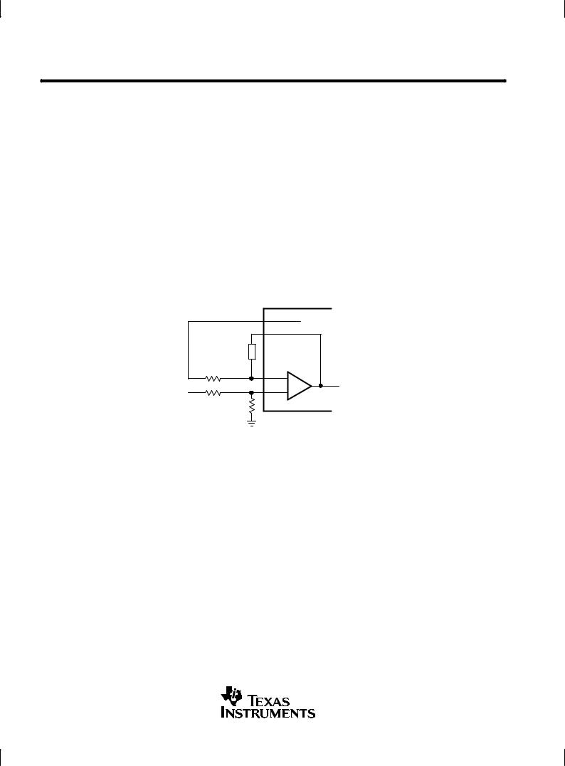
The error amplifier generates the error signal used by the PWM to adjust the power-switch duty cycle for the desired converter output voltage. The signal is generated by comparing a sample of the output voltage to the voltage reference and amplifying the difference. An external resistive divider connected between the converter output and ground, as shown in Figure 1, is generally required to obtain the output voltage sample.
The amplifier output is brought out on COMP to allow the frequency response of the amplifier to be shaped with an external RC network to stabilize the feedback loop of the converter. DC loading on the COMP output is limited to 45 μA (the maximum amplifier source current capability).
Figure 1 illustrates the sense-divider network and error-amplifier connections for converters with positive output voltages. The divider network is connected to the noninverting amplifier input because the PWM has a phase inversion; the duty cycle decreases as the error-amplifier output increases.
|
|
|
|
REF |
TL1454 |
|
|
|
|
COMP |
|
|
|
Compensation |
|
|
|
|
|
Network |
|
|
|
|
|
R3 |
|
IN ± |
_ |
|
|
|
|
||
|
|
|
|
|
|
Converter |
|
|
|
IN + |
To PWM |
VO |
|
|
+ |
||
Output |
R1 |
|
|
||
|
|
|
|
||
|
|
R2 |
|
|
|
|
|
|
|
|
|
Figure 1. Sense Divider/Error Amplifier
Configuration for Converters with Positive Outputs
The output voltage is given by:
VO + Vref 1 ) R1R2
where Vref = 1.25 V.
The dc source resistance of the error-amplifier inputs should be 10 kΩ or less and approximately matched to minimize output voltage errors caused by the input-bias current. A simple procedure for determining appropriate values for the resistors is to choose a convenient value for R3 (10 kΩ or less) and calculate R1 and R2 using:
R1 |
|
R3VO |
|
|||
+ |
V |
|
±V |
ref |
||
|
|
O |
|
|||
R2 |
|
R3VO |
||||
+ |
V |
ref |
|
|
||
|
|
|
|
|
||
|
|
|
|
|
|
|
|
|
|
|
|
|
|
4 |
POST OFFICE BOX 655303 •DALLAS, TEXAS 75265 |
|
POST OFFICE BOX 1443 •HOUSTON, TEXAS 77251±1443 |
TL1454, TL1454Y
DUAL-CHANNEL PULSE-WIDTH-MODULATION (PWM)
CONTROL CIRCUIT
SLVS086B ± APRIL 1995 ± REVISED NOVEMBER 1997
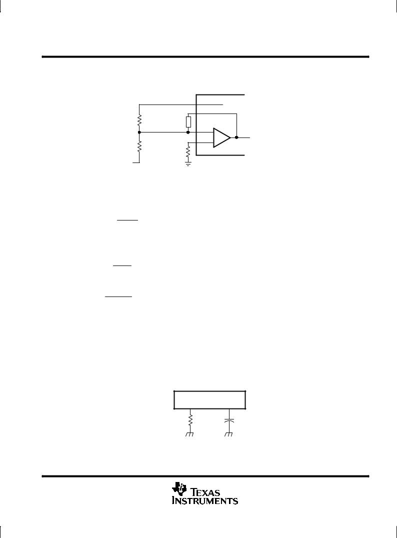
error amplifier
R1 and R2 should be tight-tolerance (±1% or better) devices with low and/or matched temperature coefficients to minimize output voltage errors. A device with a ±5% tolerance is suitable for R3.
|
REF |
|
|
COMP |
|
R2 |
Compensation |
|
|
Network |
|
|
IN ± |
_ |
|
|
|
|
IN + |
To PWM |
R1 |
|
+ |
R3 |
|
|
|
|
Converter
Output VO
Figure 2. Sense Divider/Error Amplifier Configuration for Converters with Negative Outputs
Figure 2 shows the divider network and error-amplifier configuration for negative output voltages. In general, the comments for positive output voltages also apply for negative outputs. The output voltage is given by:
V + * R1Vref
O R2
The design procedure for choosing the resistor value is to select a convenient value for R2 (instead of R3 in the procedure for positive outputs) and calculate R1 and R3 using:
R V R1 + * V2 O
ref
R + R1R2 3 R1 )R2
Values in the 10-kΩ to 20-kΩ range work well for R2. R3 can be omitted and the noninverting amplifier connected to ground in applications where the output voltage tolerance is not critical.
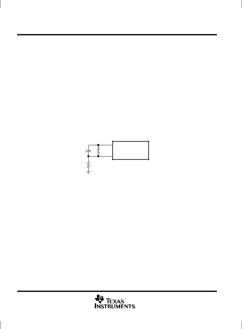
oscillator
The oscillator frequency can be set between 50 kHz and 2 MHz with a resistor connected between RT and GND and a capacitor between CT and GND (see Figure 3). Figure 6 is used to determine RT and CT for the desired operating frequency. Both components should be tight-tolerance, temperature-stable devices to minimize frequency deviation. A 1% metal-film resistor is recommended for RT, and a 10%, or better, NPO ceramic capacitor is recommended for CT.
|
TL1454 |
RT |
CT |
2 |
1 |
RT |
CT |
Figure 3. Oscillator Timing
POST OFFICE BOX 655303 •DALLAS, TEXAS 75265 |
5 |
POST OFFICE BOX 1443 •HOUSTON, TEXAS 77251±1443 |
|
TL1454, TL1454Y
DUAL-CHANNEL PULSE-WIDTH-MODULATION (PWM)
CONTROL CIRCUIT
SLVS086B ± APRIL 1995 ± REVISED NOVEMBER 1997
dead-time control (DTC) and soft start
The two PWM channels have independent dead-time control inputs so that the maximum power-switch duty cycles can be limited to less then 100%. The dead-time is set with a voltage applied to DTC; the voltage is typically obtained from a resistive divider connected between the reference and ground as shown in Figure 4. Soft start is implemented by adding a capacitor between REF and DTC.
The voltage, VDT, required to limit the duty cycle to a maximum value is given by:
VDT + VO(max) * D VO(max) * VO(min) * 0.65
where VO(max) and VO(min) are obtained from Figure 9, and D is the maximum duty cycle.
Predicting the regulator startup or rise time is complicated because it depends on many variables, including: input voltage, output voltage, filter values, converter topology, and operating frequency. In general, the output will be in regulation within two time constants of the soft-start circuit. A five-to-ten millisecond time constant usually works well for low-power converters.
The DTC input can be grounded in applications where achieving a 100% duty cycle is desirable, such as a buck converter with a very low input-to-output differential voltage. However, grounding DTC prevents the implementation of soft start, and the output voltage overshoot at power-on is likely to be very large. A better arrangement is to omit RDT1 (see Figure 4) and choose RDT2 = 47 kΩ. This configuration ensures that the duty cycle can reach 100% and still allows the designer to implement soft start using CSS.
|
16 |
REF |
|
|
|
CSS |
RDT1 |
TL1454 |
|
||
|
|
DTC |
|
RDT2 |
|
Figure 4. Dead-Time Control and Soft Start
PWM comparator
Each of the PWM comparators has dual inverting inputs. One inverting input is connected to the output of the error amplifier; the other inverting input is connected to the DTC terminal. Under normal operating conditions, when either the error-amplifier output or the dead-time control voltage is higher than that for the PWM triangle wave, the output stage is set inactive (OUT1 low and OUT2 high), turning the external power stage off.
undervoltage-lockout (UVLO) protection
The undervoltage-lockout circuit turns the output circuit off and resets the SCP latch whenever the supply voltage drops too low (to approximately 2.9 V) for proper operation. A hysteresis voltage of 200 mV eliminates false triggering on noise and chattering.
short-circuit protection (SCP)
The TL1454 SCP function prevents damage to the power switches when the converter output is shorted to ground. In normal operation, SCP comparator 1 clamps SCP to approximately 185 mV. When one of the converter outputs is shorted, the error amplifier output (COMP) will be driven below 1 V to maximize duty cycle and force the converter output back up. When the error amplifier output drops below 1 V, SCP comparator 1 releases SCP, and capacitor, CSCP, which is connected between SCP and GND, begins charging. If the error-amplifier output rises above 1 V before CSCP is charged to 1 V, SCP comparator 1 discharges CSCP and normal operation resumes. If CSCP reaches 1 V, SCP comparator 2 turns on and sets the SCP latch, which turns off the output drives and resets the soft-start circuit. The latch remains set until the supply voltage is lowered to 2 V or less, or CSCP is discharged externally.
6 |
POST OFFICE BOX 655303 •DALLAS, TEXAS 75265 |
|
POST OFFICE BOX 1443 •HOUSTON, TEXAS 77251±1443 |

TL1454, TL1454Y
DUAL-CHANNEL PULSE-WIDTH-MODULATION (PWM)
CONTROL CIRCUIT
SLVS086B ± APRIL 1995 ± REVISED NOVEMBER 1997
short-circuit protection (SCP) (continued)
The SCP time-out period must be greater than the converter start-up time or the converter will not start. Because high-value capacitor tolerances tend to be ± 20% or more and IC resistor tolerances are loose as well, it is best to choose an SCP time-out period 10-to-15 times greater than the converter startup time. The value of CSCP may be determined using Figure 6, or it can be calculated using:
CSCP |
+ TSCP |
|
|
80.3 |
|
where CSCP is in μF and TSCP is the time-out period in ms.
output stage
The output stage of the TL1454 is a totem-pole output with a maximum source/sink current rating of 40 mA and a voltage rating of 20 V. The output is controlled by a complementary output AND gate and is turned on (sourcing current for OUT1, sinking current for OUT2) when all the following conditions are met: 1) the oscillator triangle wave voltage is higher than both the DTC voltage and the error-amplifier output voltage, 2) the undervoltage-lockout circuit is inactive, and 3) the short-circuit protection circuit is inactive.
absolute maximum ratings over operating free-air temperature range (unless otherwise noted)²
Supply voltage, VCC (see Note 1) . . . . . . . . . . . . . . . . . . . . . . . . . . . . . . . . . . . . . . . |
. . . . . . . . . . . . . . . . . . . . . 23 V |
Error amplifier input voltage: IN1+, IN1±, IN2+, IN2± . . . . . . . . . . . . . . . . . . . . . . |
. . . . . . . . . . . . . . . . . . . . . 23 V |
Output voltage: OUT1, OUT2 . . . . . . . . . . . . . . . . . . . . . . . . . . . . . . . . . . . . . . . . . . . |
. . . . . . . . . . . . . . . . . . . . . 20 V |
Continuous output current: OUT1, OUT2 . . . . . . . . . . . . . . . . . . . . . . . . . . . . . . . . . |
. . . . . . . . . . . . . . . . . ± 200 mA |
Peak output current: OUT1, OUT2 . . . . . . . . . . . . . . . . . . . . . . . . . . . . . . . . . . . . . . |
. . . . . . . . . . . . . . . . . . . . . . 1 A |
Continuous total dissipation . . . . . . . . . . . . . . . . . . . . . . . . . . . . . . . . . . . . . . . . . . . |
See Dissipation Rating Table |
Operating free-air temperature range, TA: C suffix . . . . . . . . . . . . . . . . . . . . . . . . |
. . . . . . . . . . . . ±20°C to 85°C |
I suffix . . . . . . . . . . . . . . . . . . . . . . . . . |
. . . . . . . . . . . . ±40°C to 85°C |
Storage temperature range, Tstg . . . . . . . . . . . . . . . . . . . . . . . . . . . . . . . . . . . . . . . . |
. . . . . . . . . . . ±65°C to 150°C |
Lead temperature 1,6 mm (1/16 inch) from case for 10 seconds . . . . . . . . . . . . |
. . . . . . . . . . . . . . . . . . . 260°C |
²Stresses beyond those listed under ªabsolute maximum ratingsº may cause permanent damage to the device. These are stress ratings only, and functional operation of the device at these or any other conditions beyond those indicated under ªrecommended operating conditionsº is not implied. Exposure to absolute-maximum-rated conditions for extended periods may affect device reliability.
NOTE 1: All voltage values are with respect to network GND.
DISSIPATION RATING TABLE
PACKAGE |
TA ≤ 25°C |
DERATING FACTOR |
TA = 70°C |
TA = 85°C |
|
POWER RATING |
ABOVE TA = 25°C |
POWER RATING |
POWER RATING |
||
|
|||||
D |
950 mW |
7.6 mW/°C |
608 mW |
494 mW |
|
N |
1250 mW |
10.0 mW/°C |
800 mW |
650 mW |
|
PW |
500 mW |
4.0 mW/°C |
320 mW |
260 mW |
|
|
|
|
|
|
POST OFFICE BOX 655303 •DALLAS, TEXAS 75265 |
7 |
POST OFFICE BOX 1443 •HOUSTON, TEXAS 77251±1443 |
|
TL1454, TL1454Y
DUAL-CHANNEL PULSE-WIDTH-MODULATION (PWM)
CONTROL CIRCUIT
SLVS086B ± APRIL 1995 ± REVISED NOVEMBER 1997
recommended operating conditions
|
|
MIN |
MAX |
UNIT |
|
|
|
|
|
|
|
Supply voltage, VCC |
|
3.6 |
20 |
V |
|
Error amplifier common-mode input voltage |
|
± 0.2 |
1.45 |
V |
|
|
|
|
|
|
|
Output voltage, VO |
|
|
20 |
V |
|
Output current, IO |
|
|
± 40 |
mA |
|
COMP source current |
|
|
± 45 |
μA |
|
|
|
|
|
|
|
COMP sink current |
|
|
100 |
μA |
|
|
|
|
|
|
|
Reference output current |
|
|
1 |
mA |
|
|
|
|
|
|
|
COMP dc load resistance |
|
100 |
|
kΩ |
|
|
|
|
|
|
|
Timing capacitor, CT |
|
10 |
4000 |
pF |
|
Timing resistor, RT |
|
5.1 |
100 |
kΩ |
|
Oscillator frequency |
|
50 |
2000 |
kHz |
|
|
|
|
|
|
|
Operating free-air temperature, TA |
TL1454C |
± 20 |
85 |
°C |
|
|
|
|
|||
TL1454I |
± 40 |
85 |
|||
|
|
||||
|
|
|
|
|
electrical characteristics over recommended operating free-air temperature range, VCC = 6 V, fosc = 500 kHz (unless otherwise noted)
reference
|
PARAMETER |
TEST CONDITIONS |
|
TL1454 |
|
UNIT |
|
|
|
|
|
||||
|
MIN |
TYP |
MAX |
||||
|
|
|
|
|
|||
|
|
|
|
|
|
|
|
Vref |
Output voltage, REF |
IO = 1 mA, |
TA = 25°C |
1.23 |
1.25 |
1.28 |
V |
IO = 1 mA |
|
1.2 |
|
1.31 |
|||
|
|
|
|
|
|||
|
Input regulation |
VOC = 3.6 V to 20 V, |
IO = 1 mA |
|
2 |
6 |
mV |
|
Output regulation |
IO = 0.1 mA to 1 mA |
|
|
1 |
7.5 |
mV |
|
Output voltage change with temperature |
TA = TA(min) to 25°C, |
IO = 1 mA |
±12.5 |
± 1.25 |
12.5 |
mV |
|
TA = 25°C to 85°C, |
IO = 1 mA |
±12.5 |
±2.5 |
12.5 |
||
|
|
|
|||||
IOS |
Short-circuit output current |
Vref = 0 V |
|
|
30 |
|
mA |
undervoltage lockout (UVLO)
|
PARAMETER |
TEST CONDITIONS |
|
TL1454 |
|
UNIT |
|
|
|
|
|||
|
MIN |
TYP |
MAX |
|||
|
|
|
|
|||
|
|
|
|
|
|
|
VIT + |
Positive-going threshold voltage |
|
|
2.9 |
|
V |
VIT ± |
Negative-going threshold voltage |
TA = 25°C |
|
2.7 |
|
V |
Vhys |
Hysteresis, VIT + ± VIT ± |
|
100 |
200 |
|
mV |
short-circuit protection (SCP)
|
PARAMETER |
TEST CONDITIONS |
|
TL1454 |
|
UNIT |
|
|
|
|
|
||||
|
MIN |
TYP |
MAX |
||||
|
|
|
|
|
|||
|
|
|
|
|
|
|
|
VIT |
Input threshold voltage |
TA = 25°C |
|
0.95 |
1 |
1.05 |
V |
Vstby² |
Standby voltage |
No pullup |
|
140 |
185 |
230 |
mV |
VI(latched) |
Latched-mode input voltage |
|
|
60 |
120 |
mV |
|
|
|
|
|||||
VIT(COMP) |
Comparator threshold voltage |
COMP1, COMP2 |
|
1 |
|
V |
|
|
Input source current |
TA = 25°C, |
VO(SCP) = 0 |
± 5 |
± 15 |
± 20 |
μA |
² This symbol is not presently listed within EIA / JEDEC standards for semiconductor symbology.
8 |
POST OFFICE BOX 655303 •DALLAS, TEXAS 75265 |
|
POST OFFICE BOX 1443 •HOUSTON, TEXAS 77251±1443 |
 Loading...