


TLC1078IDR
Texas Instruments TLC1078IDR, TLC1078ID, TLC1078CPS, TLC1078CPSR, TLC1078CP Datasheet
...
TLC1078, TLC1078Y, TLC1079, TLC1079Y
LinCMOS µPOWER PRECISION
OPERATIONAL AMPLIFIERS
SLOS179 – FEBRUARY 1997
1
POST OFFICE BOX 655303 • DALLAS, TEXAS 75265
D
Power Dissipation as Low as 10 µW Typ Per
Amplifier
D
Operates on a Single Silver-Oxide Watch
Battery, V
DD
= 1.4 V Min
D
VIO. . . 450 µV/850 µV Max in DIP and
Small-Outline Package (TLC1078/79)
D
Input Offset Voltage Drift...0.1 µV/Month
Typ, Including the First 30 Days
D
High-impedance LinCMOS Inputs
I
IB
= 0.6 pA Typ
D
High Open-Loop Gain...800000 Typ
D
Output Drive Capability > 20 mA
D
Slew Rate...47 V/ms T yp
D
Common-Mode Input Voltage Range
Extends Below the Negative Rail
D
Output Voltage Range Includes Negative
Rail
D
On-Chip ESD-Protection Circuitry
D
Small-Outline Package Option Also
Available in Tape and Reel
description
The TLC107x operational amplifiers offer ultralow offset voltage, high gain, 1 10-kHz bandwidth,
47-V/ms slew rate, and just 150-µW power
dissipation per amplifier.
With a supply voltage of 1.4 V, common-mode
input to the negative rail, and output swing to the
negative rail, the TLC107xC is an ideal solution for
low-voltage battery-operated systems. The
20-mA output drive capability means that the
TLC107x can easily drive small resistive and large
capacitive loads when needed, while maintaining
ultra-low standby power dissipation.
Since this device is functionally compatible as well
as pin compatible with the TLC27L2/4 and
TLC27L7/9, the TLC107x easily upgrades
existing designs that can benefit from its improved
performance.
Copyright 1997, Texas Instruments Incorporated
PRODUCTION DATA information is current as of publication date.
Products conform to specifications per the terms of Texas Instruments
standard warranty. Production processing does not necessarily include
testing of all parameters.
Please be aware that an important notice concerning availability, standard warranty, and use in critical applications of
Texas Instruments semiconductor products and disclaimers thereto appears at the end of this data sheet.
LinCMOS is a trademark of Texas Instruments Incorporated.
1
2
3
4
8
7
6
5
1OUT
1IN –
1IN+
GND
V
DD
2OUT
2IN –
2IN+
3212019
910111213
4
5
6
7
8
18
17
16
15
14
NC
2OUT
NC
2IN –
NC
NC
1IN –
NC
1IN+
NC
NC
1OUT
NC
2IN +
NC
NC
NC
GND
NC
NC – No internal connection
DD
V
TLC1078
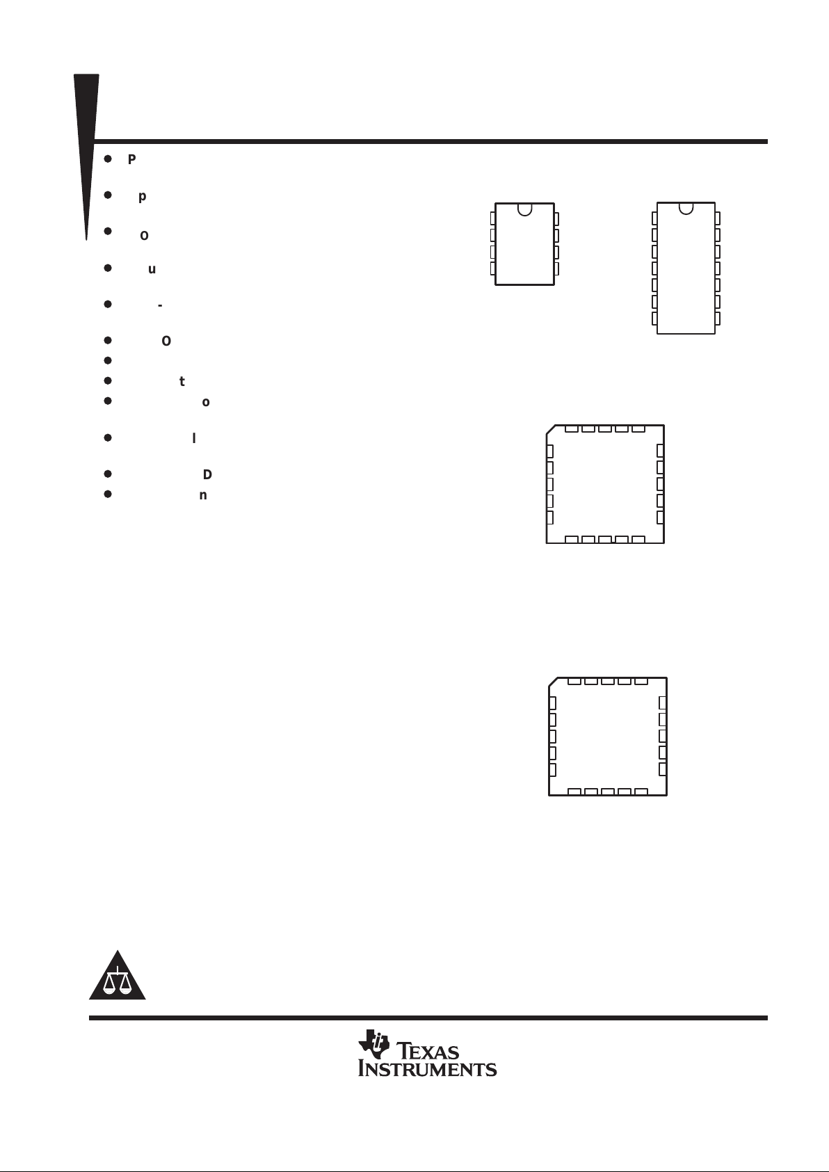
D, JG, OR P PACKAGE
(TOP VIEW)
TLC1078
FK PACKAGE
(TOP VIEW)
3212019
910111213
4
5
6
7
8
18
17
16
15
14
4IN+
NC
GND
NC
3IN+
1IN+
NC
V
DD
NC
2IN+
1IN –
1OUT
NC
3OUT
3IN –
4IN –
2IN –
2OUT
NC
4OUT
1
2
3
4
5
6
7
14
13
12
11
10
9
8
1OUT
1IN –
1IN+
V
DD
2IN+
2IN –
2OUT
4OUT
4IN –
4IN+
GND
3IN+
3IN –
3OUT
TLC1079
D, J, OR N PACKAGE
(TOP VIEW)
TLC1079
FK PACKAGE
(TOP VIEW)
TLC1078, TLC1078Y, TLC1079, TLC1079Y
LinCMOS µPOWER PRECISION
OPERATIONAL AMPLIFIERS
SLOS179 – FEBRUARY 1997
2
POST OFFICE BOX 655303 • DALLAS, TEXAS 75265
description (continued)
The TLC107x incorporates internal ESD-protection circuits that will prevent functional failures at voltages up
to 2000 V as tested under MIL-PRF-38535, Method 3015.2; however, care should be exercised when handling
these devices as exposure to ESD may result in degradation of the device parametric performance. The
TLC107x design also inhibits latch-up of the device inputs and outputs even with surge currents as large
100 mA.
The C-suffix devices are characterized for operation from 0°C to 70°C. The I-suffix devices are characterized
for operation from – 40°C to 85°C. The M-suffix devices are characterized for operation over the full military
temperature range of –55°C to 125°C. The wide range of packaging options includes small-outline and
chip-carrier versions for high-density system applications.
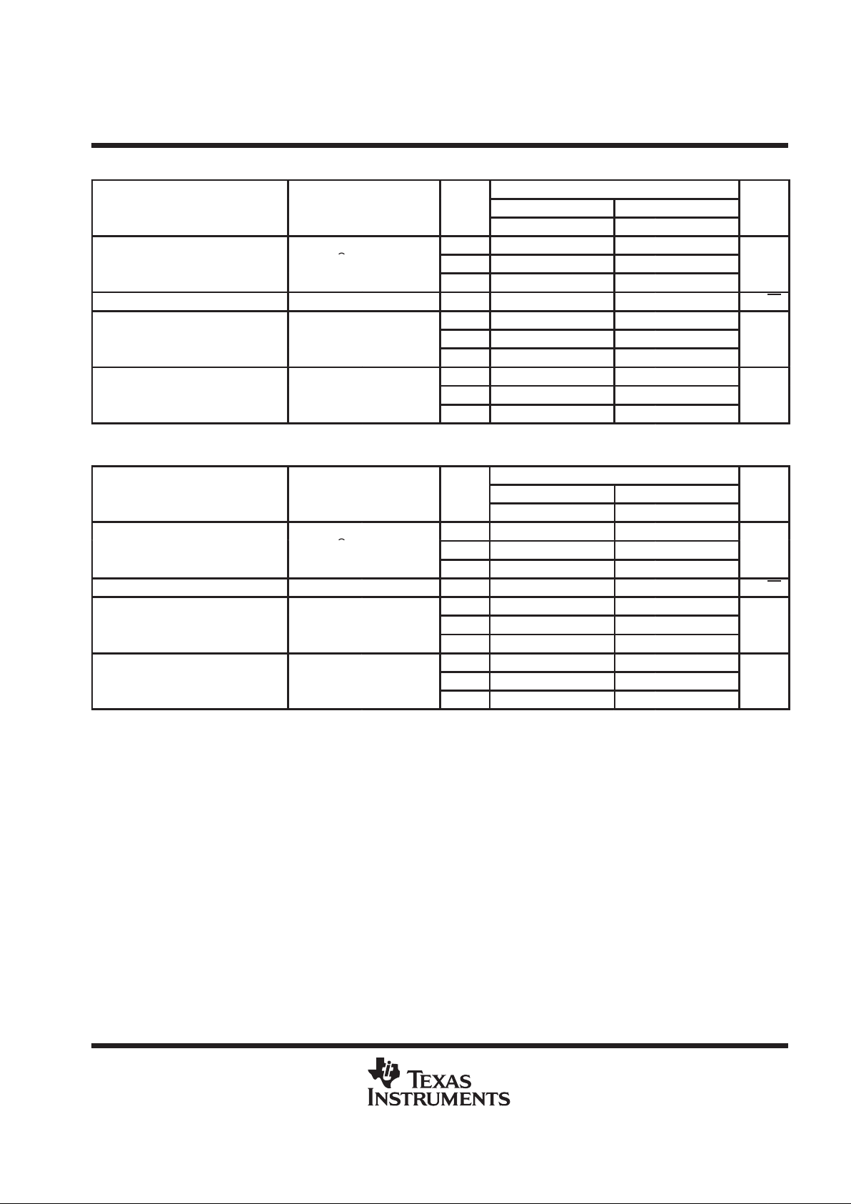
AVAILABLE OPTIONS
PACKAGED DEVICES
CHIP
T
A
SMALL OUTLINE
†
CHIP CARRIER CERAMIC DIP CERAMIC DIP PLASTIC DIP PLASTIC DIP
FORM
‡
(D)
(FK) (J) (JG) (N) (P)
(Y)
0°C to 70°C
TLC1078CD
TLC1079CD
— — — TLC1079CN TLC1078CP
TLC1078Y
TLC1079Y
–40°C to 85°C
TLC1078ID
TLC1079ID
— — — TLC1079IN TLC1078IP —
–55°C to 125°C
TLC1078MD
TLC1079MD
TLC1078MFK
TLC1079MFK
TLC1079MJ TLC1078MJG TLC1079MN TLC1078MP —
†
The D package is available taped and reeled. Add the suffix R to the device type (e.g., TLC1078CDR).
‡
Chip forms are tested 25°C only.
symbol (each amplifier)
OUT
–
+
IN–
IN+
TLC1078, TLC1078Y, TLC1079, TLC1079Y
LinCMOS µPOWER PRECISION
OPERATIONAL AMPLIFIERS
SLOS179 – FEBRUARY 1997
3
POST OFFICE BOX 655303 • DALLAS, TEXAS 75265
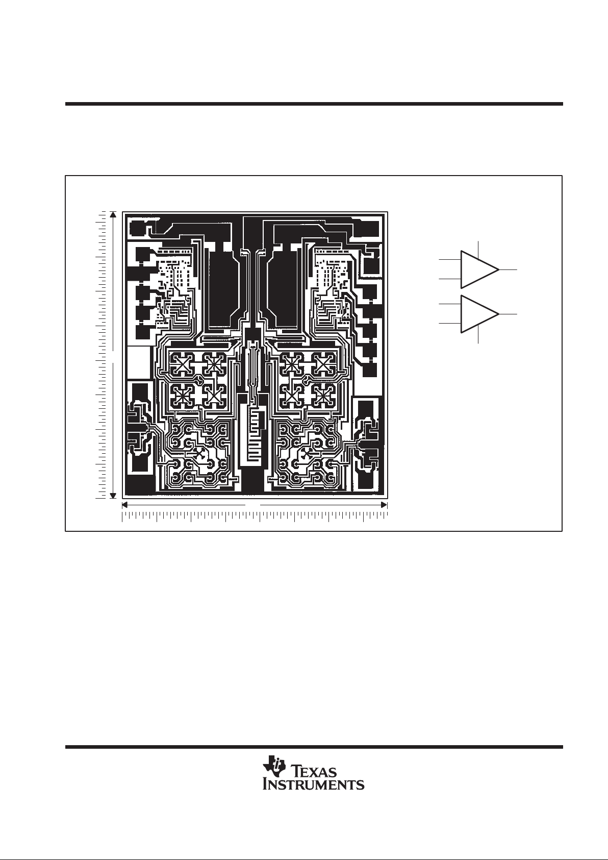
TLC1087Y chip information
This chip, when properly assembled, displays characteristics similar to the TLC1078C. Thermal compression
or ultrasonic bonding may be used on the doped-aluminum bonding pads. Chips can be mounted with
conductive epoxy or a gold-silicon preform.
BONDING PAD ASSIGNMENTS
CHIP THICKNESS: 15 MILS TYPICAL
BONDING PADS: 4 × 4 MILS MINIMUM
TJmax = 150°C
TOLERANCES ARE ±10%.
ALL DIMENSIONS ARE IN MILS.
+
–
1OUT
1IN+
1IN–
V
DD
V
DD–
/GND
(8)
(3)
(2)
(4)
+
–
2OUT
2IN+
2IN–
(5)
(6)
83
72
(1)
(5)
(4)
(3)
(2)
(6)
(7)
(8)
BONDING PAD ASSIGNMENTS
TLC1078, TLC1078Y, TLC1079, TLC1079Y
LinCMOS µPOWER PRECISION
OPERATIONAL AMPLIFIERS
SLOS179 – FEBRUARY 1997
4
POST OFFICE BOX 655303 • DALLAS, TEXAS 75265
TLC1079Y chip information
This chip, when properly assembled, display characteristics similar to the TLC1079C. Thermal compression
or ultrasonic bonding may be used on the doped-aluminum bonding pads. Chips can be mounted with
conductive epoxy or a gold-silicon preform.
BONDING PAD ASSIGNMENTS
+
–
1OUT
1IN+
1IN–
V
DD
(4)
(6)
(3)
(2)
(5)
(1)
2IN+
2IN–
2OUT
(11)
V
DD–
/GND
+
–
3OUT
3IN+
3IN–
(13)
(10)
(9)
(12)
(8)
–
+
(14)
4OUT
4IN+
4IN–
+
–
(7)
CHIP THICKNESS: 15 MILS TYPICAL
BONDING PADS: 4 × 4 MILS MINIMUM
TJmax = 150°C
TOLERANCES ARE ±10%.
ALL DIMENSIONS ARE IN MILS.
PIN (11) IS INTERNALLY CONNECTED
TO BACKSIDE OF CHIP.
130
70
(1)
(2)
(3)
(4)
(5)
(6)
(7)
(8)
(9)
(10)
(11)
(12)
(13)
(14)
TLC1078, TLC1078Y, TLC1079, TLC1079Y
LinCMOS µPOWER PRECISION
OPERATIONAL AMPLIFIERS
SLOS179 – FEBRUARY 1997
5
POST OFFICE BOX 655303 • DALLAS, TEXAS 75265
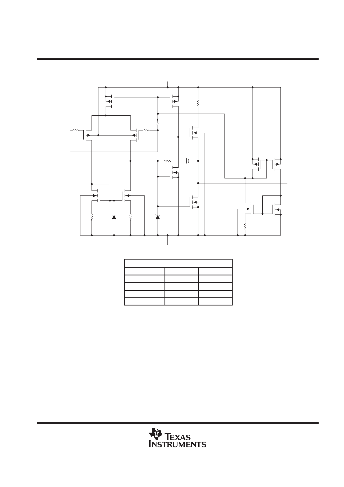
equivalent schematic (each amplifier)
R2 D1
R3
Q4Q2
Q1
R1
IN–
IN+
R4
Q5
R5
Q3 Q6
V
DD
GND
Q7
Q9
D2
C1
R6
R7
Q10
Q13
OUT
Q11
Q12
Q8
ACTUAL DEVICE COMPONENT COUNT
COMPONENT TLC1078 TLC1079
Transistors 38 76
Resistors 16 32
Diodes 12 24
Capacitors 2 4
TLC1078, TLC1078Y, TLC1079, TLC1079Y
LinCMOS µPOWER PRECISION
OPERATIONAL AMPLIFIERS
SLOS179 – FEBRUARY 1997
6
POST OFFICE BOX 655303 • DALLAS, TEXAS 75265
absolute maximum ratings over operating free-air temperature range (unless otherwise noted)
†
Supply voltage, V
DD
(see Note 1) 18 V. . . . . . . . . . . . . . . . . . . . . . . . . . . . . . . . . . . . . . . . . . . . . . . . . . . . . . . . . . . .
Differential input voltage, V
ID
(see Note 2) ±V
DD
. . . . . . . . . . . . . . . . . . . . . . . . . . . . . . . . . . . . . . . . . . . . . . . . . . .
Input voltage range, V
I
(any input) –0.3 V to V
DD
. . . . . . . . . . . . . . . . . . . . . . . . . . . . . . . . . . . . . . . . . . . . . . . . . . .
Input current, I
I
(each input) ± 5 mA. . . . . . . . . . . . . . . . . . . . . . . . . . . . . . . . . . . . . . . . . . . . . . . . . . . . . . . . . . . . . . .
Output current, I
O
(each output) ± 30 mA. . . . . . . . . . . . . . . . . . . . . . . . . . . . . . . . . . . . . . . . . . . . . . . . . . . . . . . . . .
Total current into V
DD
(see Note 3) 45 mA. . . . . . . . . . . . . . . . . . . . . . . . . . . . . . . . . . . . . . . . . . . . . . . . . . . . . . . . .
Duration of short-circuit at (or below) T
A
= 25°C (see Note 3) unlimited. . . . . . . . . . . . . . . . . . . . . . . . . . . . . . . .
Continuous total power dissipation see Dissipation Rating Table. . . . . . . . . . . . . . . . . . . . . . . . . . . . . . . . . . . . . .
Operating free-air temperature range, T
A
: C suffix 0°C to 70°C. . . . . . . . . . . . . . . . . . . . . . . . . . . . . . . . . . . . . . .
I suffix –40°C to 85°C. . . . . . . . . . . . . . . . . . . . . . . . . . . . . . . . . . . . . .
M suffix –55°C to 125°C. . . . . . . . . . . . . . . . . . . . . . . . . . . . . . . . . . . .
Storage temperature range –65°C to 150°C. . . . . . . . . . . . . . . . . . . . . . . . . . . . . . . . . . . . . . . . . . . . . . . . . . . . . . . .
Case temperature for 60 seconds: FK package 260°C. . . . . . . . . . . . . . . . . . . . . . . . . . . . . . . . . . . . . . . . . . . . . .
Lead temperature 1,6 mm (1/16 inch) from case for 10 seconds: D or P package 260°C. . . . . . . . . . . . . . . . .
Lead temperature 1,6 mm (1/16 inch) from case for 60 seconds: JG package 300°C. . . . . . . . . . . . . . . . . . . .
†
Stresses beyond those listed under “absolute maximum ratings” may cause permanent damage to the device. These are stress ratings only, and
functional operation of the device at these or any other conditions beyond those indicated under “recommended operating conditions” is not
implied. Exposure to absolute-maximum-rated conditions for extended periods may affect device reliability.
NOTES: 1. All voltage values, except differential voltages, are with respect to network ground.
2. Differential voltages are at IN+ with respect to IN–.
3. The output may be shorted to either supply. Temperature and/or supply voltages must be limited to ensure that the maximum
dissipation ratings are not exceeded.
DISSIPATION RATING TABLE
PACKAGE
TA ≤ 25°C
POWER RATING
DERATING FACTOR
ABOVE TA = 25°C
TA = 70°C
POWER RATING
TA = 85°C
POWER RATING
TA = 125°C
POWER RATING
D–8 725 mW 5.8 mW/°C 464 mW 377 mW 145 mW
D–14 950 mW 7.6 mW/°C 608 mW 494 mW 190 mW
FK 1375 mW 11.0 mW/°C 880 mW 715 mW 275 mW
J 1375 mW 11.0 mW/°C 880 mW 715 mW 275 mW
JG 1050 mW 8.4 mW/°C 672 mW 546 mW 210 mW
N 1150 mW 9.2 mW/°C 736 mW 598 mW 230 mW
P 1000 mW 8.0 mW/°C 640 mW 520 mW 200 mW
recommended operating conditions
C SUFFIX I SUFFIX M SUFFIX
MIN MAX MIN MAX MIN MAX
UNIT
Supply voltage, V
DD
1.4 16 3 16 4 16 V
p
VDD = 5 V –0.2 4 –0.2 4 0 4
Common-mode input voltage, V
IC
VDD = 10 V –0.2 9 –0.2 9 0 9
V
Operating free-air temperature, T
A
0 70 –40 85 –55 125 °C
TLC1078, TLC1078Y, TLC1079, TLC1079Y
LinCMOS µPOWER PRECISION
OPERATIONAL AMPLIFIERS
SLOS179 – FEBRUARY 1997
7
POST OFFICE BOX 655303 • DALLAS, TEXAS 75265
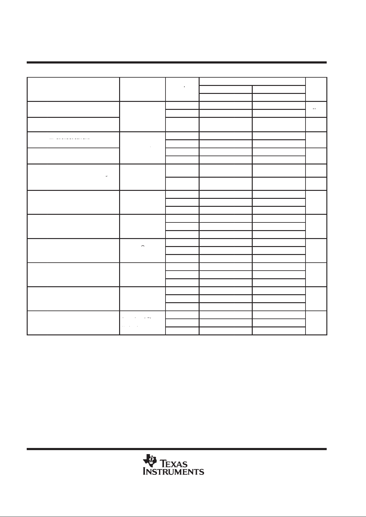
electrical characteristics at specified free-air temperature
TLC1078C
PARAMETER
TEST
T
A
†
VDD = 5 V VDD = 10 V
UNIT
CONDITIONS
A
MIN TYP MAX MIN TYP MAX
p
=
25°C 160 450 180 600
VIOInput offset voltage
V
O
= 1.4 V,
RS = 50 Ω,
Full range 800 950
µ
V
α
VIO
Temperature coefficient of input
offset voltage
VIC = 0,
RI = 1 MΩ
25°C to 70°C 1.1 1 µV/°C
p
25°C 0.1 0.1
p
IIOInput offset current (see Note 4)
V
= V
/ 2,
70°C 7 300 7 300
pA
p
ODD
,
VIC = VDD/ 2
25°C 0.6 0.7
p
IIBInput bias current (see Note 4)
70°C 40 600 50 600
pA
Common-mode input voltage
25°C
–0.2
to 4
–0.3
to 4.2
–0.2
to 9
–0.3
to 9.2
V
V
ICR
g
range (see Note 5)
Full range
–0.2
to 3.5
–0.2
to 8.5
V
25°C 3.2 4.1 8.2 8.9
V
OH
High-level output voltage
VID = 100 mV ,
0°C 3.2 4.1 8.2 8.9
V
RL= 1 MΩ
70°C 3.2 4.2 8.2 8.9
25°C 0 25 0 25
V
OL
Low-level output voltage
VID = –100 mV ,
0°C 0 25 0 25
mV
I
OL
=
0
70°C 0 25 0 25
25°C 250 525 500 850
A
VD
Large-signal differential voltage
p
RL= 1 MΩ,
0°C 250 680 500 1010
V/mV
am lification
See Note 6
70°C 200 380 350 660
25°C 70 95 75 97
CMRR Common-mode rejection ratio VIC = V
ICR
min
0°C 70 95 75 97
dB
70°C 70 95 75 97
25°C 75 98 75 98
k
SVR
Supply-voltage rejection ratio
VO = 1.4 V
0°C 75 98 75 98
dB
(∆VDD/∆VIO)
70°C 75 98 75 98
V
= V
/ 2
,
25°C 20 34 29 46
I
DD
Supply current (two amplifiers)
V
O
VDD/ 2,
VIC = VDD/ 2,
0°C 24 42 36 66
µA
No load
70°C 16 28 22 40
†
Full range is 0°C to 70°C.
NOTES: 4. The typical values of input bias current and input offset current below 5 pA were determined mathematically .
5. This range also applies to each input individually.
6. At VDD = 5 V. VO = 0.25 V to 2 V; at VDD = 10 V, VO = 1 V to 6 V.
TLC1078, TLC1078Y, TLC1079, TLC1079Y
LinCMOS µPOWER PRECISION
OPERATIONAL AMPLIFIERS
SLOS179 – FEBRUARY 1997
8
POST OFFICE BOX 655303 • DALLAS, TEXAS 75265
electrical characteristics at specified free-air temperature
TLC1079C
PARAMETER TEST CONDITIONS T
A
†
VDD = 5 V VDD = 10 V
UNIT
MIN TYP MAX MIN TYP MAX
p
25°C 190 850 200 1150
VIOInput offset voltage
VO = 1.4 V, VIC = 0,
Full range
1200 1500
µ
V
α
VIO
T emperature coef ficient of
input offset voltage
RS = 50 Ω, RI = 1 MΩ
25°C to
70°C
1.1 1 µV/°C
Input offset current
25°C 0.1 0.1
p
I
IO
(see Note 4)
V
= V
/ 2,
70°C 7 300 7 300
pA
Input bias current
ODD
,
VIC = VDD/ 2
25°C 0.6 0.7
p
I
IB
(see Note 4)
70°C 40 600 50 600
pA
Common mode input
25°C
–0.2
to 4
–0.3
to 4.2
–0.2
to 9
–0.3
to 9.2
V
V
ICR
voltage range (see Note 5)
Full range
–0.2
to 3.5
–0.2
to 8.5
V
25°C 3.2 4.1 8.2 8.9
V
OH
High-level output voltage
VID = 100 mV ,
0°C 3.2 4.1 8.2 8.9
V
R
L
= 1
MΩ
70°C 3.2 4.2 8.2 8.9
25°C 0 25 0 25
V
OL
Low-level output voltage
VID = –100 mV ,
0°C 0 25 0 25
mV
I
OL
=
0
70°C 0 25 0 25
25°C 250 525 500 850
A
VD
Large-signal differential
p
RL = 1 MΩ, See Note 6
0°C 250 700 500 1010
V/mV
voltage am lification
70°C 200 380 350 660
25°C 70 95 75 97
CMRR
Common mode rejection
VIC = V
ICR
min
0°C 70 95 75 97
dB
ratio
70°C 70 95 75 97
25°C 75 98 75 98
k
SVR
Supply-voltage rejection
VDD = 5 V to 10 V,
0°C 75 98 75 98
dB
ratio (∆VDD/∆VIO)
V
O
= 1.4
V
70°C 75 98 75 98
25°C 40 68 57 92
I
DD
S
upply current (four
p
V
O
=
VDD/ 2
,
=
0°C 48 84 72 132
µA
am lifiers)
V
IC
=
VDD/ 2
, No
load
70°C 31 56 44 80
†
Full range is 0°C to 70°C.
NOTES: 4. The typical values of input bias current and input offset current below 5 pA were determined mathematically.
5. This range also applies to each input individually.
6. At VDD = 5 V, VO = 0.25 V to 2 V; at VDD = 10 V, VO = 1 V to 6 V.
TLC1078, TLC1078Y, TLC1079, TLC1079Y
LinCMOS µPOWER PRECISION
OPERATIONAL AMPLIFIERS
SLOS179 – FEBRUARY 1997
9
POST OFFICE BOX 655303 • DALLAS, TEXAS 75265
operating characteristics at specified free-air temperature
TLC1078C
PARAMETER TEST CONDITIONS T
A
VDD = 5 V VDD = 10 V
UNIT
MIN TYP MAX MIN TYP MAX
25°C 32 47
SR Slew rate at unity gain
RL = 1 MΩ,
CL = 20 pF,
0°C 35 51
V/ms
V
I(PP)
= 1 V,
See Figure 1
70°C 27 38
VnEquivalent input noise voltage f = 1 kHz, RS = 20 Ω 25°C 68 68 nV/√Hz
25°C 85 110
B1Unity-gain bandwidth CL = 20 pF, See Figure 2
0°C
100 125
kHz
70°C 65 90
25°C 34° 38°
φmPhase margin at unity gain CL = 20 pF, See Figure 2
0°C
36° 40°
70°C 30° 34°
operating characteristics at specified free-air temperature
TLC1079C
PARAMETER TEST CONDITIONS T
A
VDD = 5 V VDD = 10 V
UNIT
MIN TYP MAX MIN TYP MAX
25°C 32 47
SR Slew rate at unity gain
RL = 1 MΩ,
CL = 20 pF,
0°C 35 51
V/ms
V
I(PP)
= 1 V,
See Figure 1
70°C 27 38
VnEquivalent input noise voltage f = 1 kHz, RS = 20 Ω 25°C 68 68 nV/√Hz
25°C 85 110
B1Unity-gain bandwidth CL = 20 pF, See Figure 2
0°C
100 125
kHz
70°C 65 90
25°C 34° 38°
φmPhase margin at unity gain CL = 20 pF, See Figure 2
0°C
36° 40°
70°C 30° 34°
TLC1078, TLC1078Y, TLC1079, TLC1079Y
LinCMOS µPOWER PRECISION
OPERATIONAL AMPLIFIERS
SLOS179 – FEBRUARY 1997
10
POST OFFICE BOX 655303 • DALLAS, TEXAS 75265
electrical characteristics at specified free-air temperature
TLC1078I
PARAMETER
TEST
T
A
†
VDD = 5 V VDD = 10 V
UNIT
CONDITIONS
A
MIN TYP MAX MIN TYP MAX
p
25°C 160 450 180 600
VIOInput offset voltage
VO = 1.4 V,
Full range 950 1100
µ
V
α
VIO
Temperature coefficient of input
offset voltage
R
S
= 50 Ω,
VIC = 0, RI = 1 MΩ
25°C to 85°C 1.1 1 µV/°C
Input offset current
25°C 0.1 0.1
p
I
IO
In ut offset current
(see Note 4)
V
= V
/ 2,
85°C 24 1000 26 1000
pA
p
ODD
,
VIC = VDD/ 2
25°C 0.6 0.7
p
IIBInput bias current (see Note 4)
85°C 200 2000 220 2000
pA
Common-mode input voltage
25°C
–0.2
to 4
–0.3
to 4.2
–0.2
to 9
–0.3
to 9.2
V
V
ICR
g
range (see Note 5)
Full range
–0.2
to 3.5
–0.2
to 8.5
V
25°C 3.2 4.1 8.2 8.9
V
OH
High-level output voltage
VID = 100 mV ,
–40°C 3.2 4.1 8.2 8.9
V
R
L
= 1
MΩ
85°C 3.2 4.2 8.2 8.9
25°C 0 25 0 25
V
OL
Low-level output voltage
VID = –100 mV ,
–40°C 0 25 0 25
mV
I
OL
=
0
85°C 0 25 0 25
25°C 250 525 500 850
A
VD
Large-signal differential voltagepRL = 1 MΩ,
–40°C 250 900 500 1550
V/mV
am lification
See Note 6
85°C 150 300 250 585
25°C 70 95 75 97
CMRR Common-mode rejection ratio VIC = V
ICR
min
–40°C 70 95 75 97
dB
85°C 70 95 75 97
25°C 75 98 75 98
k
SVR
Supply-voltage rejection ratio
VO = 1.4 V
–40°C 75 98 75 98
dB
(∆VDD/∆VIO)
85°C 75 98 75 98
V
= V
/ 2
,
25°C 20 34 29 46
I
DD
Supply current (two amplifiers)
V
O
VDD/ 2,
VIC = VDD/ 2,
–40°C 31 54 50 86
µA
No load
85°C 15 26 20 36
†
Full range is –40°C to 80°C.
NOTES: 4. The typical values of input bias current and input offset current below 5 pA were determined mathematically.
5. This range also applies to each input individually.
6. At VDD = 5 V, VO = 0.25 V to 2 V; at VDD = 10 V, VO = 1 V to 6 V.
 Loading...