


Texas Instruments TL16C552APN, TL16C552AMHV, TL16C552AMHVB, TL16C552AIFN, TL16C552AFNR Datasheet
...TL16C552A, TL16C552AM DUAL ASYNCHRONOUS COMMUNICATIONS ELEMENT WITH FIFO
SLLS189D ± NOVEMBER 1994 ± REVISED JANUARY 1999
DIBM PC/AT Compatible
DTwo TL16C550 ACEs
DEnhanced Bidirectional Printer Port
D16-Byte FIFOs Reduce CPU Interrupts
DUp to 16-MHz Clock Rate for up to 1-Mbaud Operation
DTransmit, Receive, Line Status, and Data Set Interrupts on Each Channel Independently Controlled
DIndividual Modem Control Signals for Each Channel
DProgrammable Serial Interface Characteristics for Each Channel:
±5-, 6-, 7-, or 8-Bit Characters
±Even, Odd, or No Parity Bit Generation and Detection
±1-, 1-1/2-, or 2-Stop Bit Generation
D3-State Outputs Provide TTL Drive for the Data and Control Bus on Each Channel
DHardware and Software Compatible With TL16C452
HV or FN PACKAGE (TOP VIEW)
|
RXRDY0 |
DCD1 |
GND |
RI1 |
DSR1 |
CLK |
CS1 |
TRI |
PEMD |
ACK |
PE BUSY |
SLCT |
DD |
ERR |
SIN1 |
RXRDY1 |
|
|
V |
|
|||||||||||||||
SOUT1 |
9 |
8 |
7 |
6 |
5 |
4 |
3 |
2 |
1 |
68 67 66 65 64 63 62 61 |
INT1 |
||||||
10 |
|
|
|
|
|
|
|
|
|
|
|
|
|
|
60 |
||
DTR1 |
11 |
|
|
|
|
|
|
|
|
|
|
|
|
|
|
59 |
INT2 |
RTS1 |
12 |
|
|
|
|
|
|
|
|
|
|
|
|
|
|
58 |
SLIN |
CTS1 |
13 |
|
|
|
|
|
|
|
|
|
|
|
|
|
|
57 |
INIT |
DB0 |
14 |
|
|
|
|
|
|
|
|
|
|
|
|
|
|
56 |
AFD |
DB1 |
15 |
|
|
|
|
|
|
|
|
|
|
|
|
|
|
55 |
STB |
DB2 |
16 |
|
|
|
|
|
|
|
|
|
|
|
|
|
|
54 |
GND |
DB3 |
17 |
|
|
|
|
|
|
|
|
|
|
|
|
|
|
53 |
PD0 |
DB4 |
18 |
|
|
|
|
|
|
|
|
|
|
|
|
|
|
52 |
PD1 |
DB5 |
19 |
|
|
|
|
|
|
|
|
|
|
|
|
|
|
51 |
PD2 |
DB6 |
20 |
|
|
|
|
|
|
|
|
|
|
|
|
|
|
50 |
PD3 |
DB7 |
21 |
|
|
|
|
|
|
|
|
|
|
|
|
|
|
49 |
PD4 |
TXRDY0 |
22 |
|
|
|
|
|
|
|
|
|
|
|
|
|
|
48 |
PD5 |
VDD |
23 |
|
|
|
|
|
|
|
|
|
|
|
|
|
|
47 |
PD6 |
RTS0 |
24 |
|
|
|
|
|
|
|
|
|
|
|
|
|
|
46 |
PD7 |
DTR0 |
25 |
|
|
|
|
|
|
|
|
|
|
|
|
|
|
45 |
INT0 |
SOUT0 |
26 |
|
|
|
|
|
|
|
|
|
|
|
|
|
|
44 |
BDO |
|
27 |
28 29 30 31 32 33 34 35 36 37 38 39 40 41 42 43 |
|
||||||||||||||
|
GND |
CTS0 |
DCD0 |
RI0 |
DSR0 |
CS0 |
A2 |
A1 |
A0 |
IOW |
IOR CS2 |
RESET |
DD |
SIN0 |
TXRDY1 |
ENIRQ |
|
|
V |
|
|||||||||||||||
Please be aware that an important notice concerning availability, standard warranty, and use in critical applications of Texas Instruments semiconductor products and disclaimers thereto appears at the end of this data sheet.
IBM PC/AT is a trademark of International Business Machines Corporation.
PRODUCTION DATA information is current as of publication date. Products conform to specifications per the terms of Texas Instruments standard warranty. Production processing does not necessarily include testing of all parameters.
Copyright 1999, Texas Instruments Incorporated
POST OFFICE BOX 655303 •DALLAS, TEXAS 75265 |
1 |

TL16C552A, TL16C552AM
DUAL ASYNCHRONOUS COMMUNICATIONS ELEMENT
WITH FIFO
SLLS189D ± NOVEMBER 1994 ± REVISED JANUARY 1999
PN PACKAGE (TOP VIEW)
|
|
|
|
|
|
|
|
|
|
|
|
NC |
INT1 |
INT2 |
|
SLIN |
|
INIT |
|
AFD |
|
STB GND PD0 PD1 PD2 PD3 |
PD4 PD5 |
PD6 |
PD7 |
INT0 |
|
BDO NC |
NC |
|
|
|
|
|
|
|
|
|
||||||||||||||||||||||||||
|
|
|
|
|
|
|
|
|
|
|
|
|
|
|
|
|
|
|
|
|
|
|
|
|
|
|||||||||||||||||||||||||||||||||||||||
|
|
|
|
|
|
|
|
|
|
|
|
|
|
|
|
|
|
|
|
|
|
|
|
|
|
|
|
|
|
|
|
|
|
|
|
|
|
|
|
|
|
|
|
|
|
|
|
|
|
|
|
|
|
|
|
|
|
|
|
|
|
|
|
|
|
|
|
|
|
|
|
|
|
|
|
|
|
|
|
|
|
|
|
|
|
|
|
|
|
|
|
|
|
|
|
|
|
|
|
|
|
|
|
|
|
|
|
|
|
|
|
|
|
|
|
|
|
|
|
|
|
|
|
|
|
|
|
|
|
|
|
|
|
NC |
|
|
|
80 79 78 |
|
|
77 76 75 74 73 72 71 70 69 68 67 66 65 64 63 62 61 |
|
|
|
|
NC |
||||||||||||||||||||||||||||||||||||||||||||||||
|
|
|
|
|
|
|
|
|
|
|
||||||||||||||||||||||||||||||||||||||||||||||||||||||
|
|
|
|
|
|
1 |
|
|
|
|
|
|
|
|
|
|
|
|
|
|
|
|
|
|
|
|
|
|
|
|
|
|
|
|
|
|
|
|
|
|
|
|
|
|
|
60 |
|
|
||||||||||||||||
|
|
|
|
|
|
|
|
|
|
|
|
|
|
|
|
|
|
|
|
|
|
|
|
|
|
|
|
|
|
|
|
|
|
|
|
|
|
|
|
|
|
|
|
|
|
|
||||||||||||||||||
|
|
|
|
NC |
|
|
|
|
|
|
|
|
|
|
|
|
|
|
|
|
|
|
|
|
|
|
|
|
|
|
|
|
|
|
|
|
|
|
|
|
|
|
|
|
|
|
|
|
|
|
|
|
|
|
|
|
|
|
|
|
|
|||
|
|
|
|
|
|
2 |
|
|
|
|
|
|
|
|
|
|
|
|
|
|
|
|
|
|
|
|
|
|
|
|
|
|
|
|
|
|
|
|
|
|
|
|
|
|
|
59 |
|
|
ENIRQ |
|
|
|||||||||||||
|
|
|
|
|
|
|
|
|
|
|
|
|
|
|
|
|
|
|
|
|
|
|
|
|
|
|
|
|
|
|
|
|
|
|
|
|
|
|
|
|
|
|
|
|
|
|
|
|
|
|
|
|
|
|
|
|
|
|
|
|
|
|
|
|
RXRDY1 |
|
|
|
|
|
|
3 |
|
|
|
|
|
|
|
|
|
|
|
|
|
|
|
|
|
|
|
|
|
|
|
|
|
|
|
|
|
|
|
|
|
|
|
|
|
|
|
58 |
|
|
TXRDY1 |
||||||||||||||
|
SIN1 |
|
|
4 |
|
|
|
|
|
|
|
|
|
|
|
|
|
|
|
|
|
|
|
|
|
|
|
|
|
|
|
|
|
|
|
|
|
|
|
|
|
|
|
57 |
|
|
SIN0 |
|||||||||||||||||
|
|
|
|
|
|
|
|
|
|
|
|
|
|
|
|
|
|
|
|
|
|
|
|
|
|
|
|
|
|
|
|
|
|
|
|
|
|
|
|
|
|
|
|
|||||||||||||||||||||
|
|
|
|
|
|
|
|
|
|
|
|
|
|
|
|
|
|
|
|
|
|
|
|
|
|
|
|
|
|
|
|
|
|
|
|
|
|
|
|
|
|
|
|
|
|
|
|
|
|
|
|
|
|
|
|
VDD |
||||||||
|
|
ERR |
|
|
|
|
|
|
5 |
|
|
|
|
|
|
|
|
|
|
|
|
|
|
|
|
|
|
|
|
|
|
|
|
|
|
|
|
|
|
|
|
|
|
|
|
|
|
|
56 |
|
|
|||||||||||||
|
|
|
|
|
|
|
|
|
|
|
|
|
|
|
|
|
|
|
|
|
|
|
|
|
|
|
|
|
|
|
|
|
|
|
|
|
|
|
|
|
|
|
|
|
|
|
|
|
||||||||||||||||
|
|
VDD |
|
|
6 |
|
|
|
|
|
|
|
|
|
|
|
|
|
|
|
|
|
|
|
|
|
|
|
|
|
|
|
|
|
|
|
|
|
|
|
|
|
|
|
55 |
|
|
RESET |
|
|||||||||||||||
|
|
|
|
|
|
|
|
|
|
|
|
|
|
|
|
|
|
|
|
|
|
|
|
|
|
|
|
|
|
|
|
|
|
|
|
|
|
|
|
|
|
|
|
|
|
|||||||||||||||||||
|
SLCT |
|
|
7 |
|
|
|
|
|
|
|
|
|
|
|
|
|
|
|
|
|
|
|
|
|
|
|
|
|
|
|
|
|
|
|
|
|
|
|
|
|
|
|
54 |
|
|
CS2 |
|
|
|
|
|
|
|||||||||||
BUSY |
|
|
|
|
|
|
|
|
|
|
|
|
|
|
|
|
|
|
|
|
|
|
|
|
|
|
|
|
|
|
|
|
|
|
|
|
|
|
|
|
|
|
|
|
|
|
|
|
|
|
|
|
|
|
|
|
|
|||||||
|
|
8 |
|
|
|
|
|
|
|
|
|
|
|
|
|
|
|
|
|
|
|
|
|
|
|
|
|
|
|
|
|
|
|
|
|
|
|
|
|
|
|
53 |
|
|
IOR |
|
|
|
|
|
|
|
||||||||||||
|
|
|
|
PE |
|
|
|
|
|
|
|
|
|
|
|
|
|
|
|
|
|
|
|
|
|
|
|
|
|
|
|
|
|
|
|
|
|
|
|
|
|
|
|
|
|
|
|
|
|
|
|
|
|
|
|
|
|
|
|
|
|
|||
|
|
|
|
|
|
9 |
|
|
|
|
|
|
|
|
|
|
|
|
|
|
|
|
|
|
|
|
|
|
|
|
|
|
|
|
|
|
|
|
|
|
|
|
|
|
|
52 |
|
|
IOW |
|
|
|
|
|
||||||||||
|
|
|
|
|
|
|
|
|
|
|
|
|
|
|
|
|
|
|
|
|
|
|
|
|
|
|
|
|
|
|
|
|
|
|
|
|
|
|
|
|
|
|
|
|
|
|
|
|
|
|
|
|
|
|
|
A0 |
||||||||
|
|
ACK |
|
|
|
|
10 |
|
|
|
|
|
|
|
|
|
|
|
|
|
|
|
|
|
|
|
|
|
|
|
|
|
|
|
|
|
|
|
|
|
|
|
|
|
|
|
51 |
|
|
|||||||||||||||
PEMD |
|
|
11 |
|
|
|
|
|
|
|
|
|
|
|
|
|
|
|
|
|
|
|
|
|
|
|
|
|
|
|
|
|
|
|
|
|
|
|
|
|
|
|
50 |
|
|
A1 |
||||||||||||||||||
|
|
|
|
|
|
|
|
|
|
|
|
|
|
|
|
|
|
|
|
|
|
|
|
|
|
|
|
|
|
|
|
|
|
|
|
|
|
|
|
|
|
|
||||||||||||||||||||||
|
|
|
TRI |
|
|
12 |
|
|
|
|
|
|
|
|
|
|
|
|
|
|
|
|
|
|
|
|
|
|
|
|
|
|
|
|
|
|
|
|
|
|
|
|
|
|
|
49 |
|
|
A2 |
|||||||||||||||
|
|
|
|
|
|
|
|
|
|
|
|
|
|
|
|
|
|
|
|
|
|
|
|
|
|
|
|
|
|
|
|
|
|
|
|
|
|
|
|
|
|
|
|
|
|
|||||||||||||||||||
|
|
|
|
|
|
|
|
|
|
|
|
|
|
|
|
|
|
|
|
|
|
|
|
|
|
|
|
|
|
|
|
|
|
|
|
|
|
|
|
|
|
|
|
|
|
|
|
|
|
|
|
|
|
|
|
|
|
|
|
|
|
|
|
|
|
|
|
CS1 |
|
|
|
|
13 |
|
|
|
|
|
|
|
|
|
|
|
|
|
|
|
|
|
|
|
|
|
|
|
|
|
|
|
|
|
|
|
|
|
|
|
|
|
|
|
48 |
|
|
CS0 |
|
|
|
||||||||||
|
|
|
|
|
|
|
|
|
|
|
|
|
|
|
|
|
|
|
|
|
|
|
|
|
|
|
|
|
|
|
|
|
|
|
|
|
|
|
|
|
|
|
|
|
|
|
|
|
|
|
|
|
|
|
||||||||||
|
|
CLK |
|
|
|
|
|
|
|
|
|
|
|
|
|
|
|
|
|
|
|
|
|
|
|
|
|
|
|
|
|
|
|
|
|
|
|
|
|
|
|
|
|
|
|
|
|
|
|
|
|
|
|
|
|
|
|
|
||||||
|
|
|
|
14 |
|
|
|
|
|
|
|
|
|
|
|
|
|
|
|
|
|
|
|
|
|
|
|
|
|
|
|
|
|
|
|
|
|
|
|
|
|
|
|
47 |
|
|
DSR0 |
|
|
|
||||||||||||||
|
|
|
|
|
|
|
|
|
|
|
|
|
|
|
|
|
|
|
|
|
|
|
|
|
|
|
|
|
|
|
|
|
|
|
|
|
|
|
|
|
|
|
|
|
|
|
|
|
|
|
|
|
|
|
|
|
|
|
|
|
|
|
|
|
|
DSR1 |
|
|
|
|
|
|
15 |
|
|
|
|
|
|
|
|
|
|
|
|
|
|
|
|
|
|
|
|
|
|
|
|
|
|
|
|
|
|
|
|
|
|
|
|
|
|
|
46 |
|
|
RI0 |
|
|
|
|
|
|
|
|
|||||
|
|
|
|
|
|
|
|
|
|
|
|
|
|
|
|
|
|
|
|
|
|
|
|
|
|
|
|
|
|
|
|
|
|
|
|
|
|
|
|
|
|
|
|
|
|
|
|
|
|
|
|
|
|
|
|
|
|
|
|
|
|
|
|
|
|
|
|
|
RI1 |
|
|
|
|
|
16 |
|
|
|
|
|
|
|
|
|
|
|
|
|
|
|
|
|
|
|
|
|
|
|
|
|
|
|
|
|
|
|
|
|
|
|
|
|
|
|
45 |
|
|
DCD0 |
|
|
|
||||||||
|
GND |
|
|
|
|
|
|
|
|
|
|
|
|
|
|
|
|
|
|
|
|
|
|
|
|
|
|
|
|
|
|
|
|
|
|
|
|
|
|
|
|
|
|
|
|
|
|
|
|
|
|
|
|
|
|
|
|
|||||||
|
|
|
17 |
|
|
|
|
|
|
|
|
|
|
|
|
|
|
|
|
|
|
|
|
|
|
|
|
|
|
|
|
|
|
|
|
|
|
|
|
|
|
|
44 |
|
|
CTS0 |
|
|
|
|
||||||||||||||
|
|
|
|
|
|
|
|
|
|
|
|
|
|
|
|
|
|
|
|
|
|
|
|
|
|
|
|
|
|
|
|
|
|
|
|
|
|
|
|
|
|
|
|
|
|
|
|
|
|
|
|
|
|
|
|
GND |
||||||||
|
DCD1 |
|
|
|
|
18 |
|
|
|
|
|
|
|
|
|
|
|
|
|
|
|
|
|
|
|
|
|
|
|
|
|
|
|
|
|
|
|
|
|
|
|
|
|
|
|
43 |
|
|
||||||||||||||||
|
|
|
|
|
|
|
|
|
|
|
|
|
|
|
|
|
|
|
|
|
|
|
|
|
|
|
|
|
|
|
|
|
|
|
|
|
|
|
|
|
|
|
|
|
|
|
|
|||||||||||||||||
|
|
|
|
|
|
|
|
|
|
|
|
|
|
|
|
|
|
|
|
|
|
|
|
|
|
|
|
|
|
|
|
|
|
|
|
|
|
|
|
|
|
|
|
|
|
|
|
|
|
|
|
|
|
|
|
NC |
||||||||
RXRDY0 |
|
|
|
|
19 |
|
|
|
|
|
|
|
|
|
|
|
|
|
|
|
|
|
|
|
|
|
|
|
|
|
|
|
|
|
|
|
|
|
|
|
|
|
|
|
42 |
|
|
|||||||||||||||||
|
|
|
|
|
|
|
|
|
|
|
|
|
|
|
|
|
|
|
|
|
|
|
|
|
|
|
|
|
|
|
|
|
|
|
|
|
|
|
|
|
|
|
|
|
|
|
||||||||||||||||||
|
|
|
|
NC |
|
20 |
|
|
|
|
|
|
|
|
|
|
|
|
|
|
|
|
|
|
|
|
|
|
|
|
|
|
|
|
|
|
|
|
|
|
|
|
|
|
|
41 |
|
|
NC |
|||||||||||||||
|
|
|
|
|
|
|
|
|
|
|
|
|
|
|
|
|
|
|
|
|
|
|
|
|
|
|
|
|
|
|
|
|
|
|
|
|
|
|
|
|
|
|
|
|
|
|||||||||||||||||||
|
|
|
|
|
|
|
|
|
|
|
21 22 23 24 25 26 27 28 29 30 31 32 33 34 35 36 37 38 39 |
|
40 |
|
|
|
|
|
|
|
|
|
|
|
|
|
||||||||||||||||||||||||||||||||||||||
|
|
|
|
|
|
|
|
|
|
|
|
|
|
|
|
|
|
|
|
|
|
|
|
|
|
|
|
|
|
|
|
|
|
|
|
|
|
|
|
|
|
|
|
|
|
|
|
|
|
|
|
|
|
|
|
|
|
|
|
|
|
|||
|
|
|
|
|
|
|
|
|
|
|
|
NC |
NC |
SOUT1 |
DTR1 |
|
RTS1 CTS1 DB0 DB1 DB2 DB3 DB4 DB5 |
DB6 DB7 |
TXRDY0 |
V |
RTS0 |
|
DTR0 SOUT0 |
NC |
|
|
|
|
|
|
|
|
|
|||||||||||||||||||||||||||||||
|
|
|
|
|
|
|
|
|
|
|
|
|
|
|
|
|
|
|
|
|
|
|
|
|
|
|
|
|
|
|
|
|
|
|
|
|
|
|
|
|
|
|
|
DD |
|
|
|
|
|
|
|
|
|
|
|
|
|
|
|
|
|
|
|
|
|
|
|
|
|
|
|
|
|
|
|
|
|
|
|
|
|
|
|
|
|
|
|
|
|
|
|
|
|
|
|
|
|
|
|
|
|
|
|
|
|
|
|
|
|
|
|
|
|
|
|
|
|
|
|
|
|
|
|
|
|
|
|
|
|
|
|
|
|
|
|
|
|
|
|
|
|
|
|
|
|
|
|
|
|
|
|
|
|
|
|
|
|
|
|
|
|
|
|
|
|
|
|
|
|
|
|
|
|
|
|
|
|
|
|
|
|
|
|
|
|
|
|
|
|
|
|
|
|
|
description
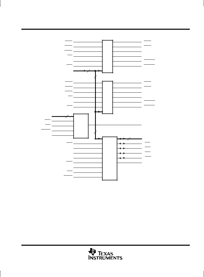
The TL16C552A is an enhanced dual-channel version of the popular TL16C550B asynchronous communications element (ACE). The device serves two serial input/output interfaces simultaneously in microcomputer or microprocessor-based systems. Each channel performs serial-to-parallel conversion on data characters received from peripheral devices or modems and parallel-to-serial conversion on data characters transmitted by the CPU. The complete status of each channel of the dual ACE can be read at any time during functional operation by the CPU. The information obtained includes the type and condition of the transfer operations being performed and the error conditions encountered.
In addition to its dual communications interface capabilities, the TL16C552A provides the user with a bidirectional parallel data port that fully supports the parallel Centronics-type printer interface. The parallel port and the two serial ports provide IBM PC/AT-compatible computers with a single device to serve the three system ports. A programmable baud rate generator that can divide the timing reference clock input by a divisor between 1 and (216 ± 1) is included.
The TL16C552A is available in a 68-pin plastic-leaded chip-carrier (FN) package, a 48-pin TQFP (PN) package, and the 80-pin TQFP (PN) package. The TL16C552AM is available in a 68-pin ceramic quad flat (HV) package.
2 |
POST OFFICE BOX 655303 •DALLAS, TEXAS 75265 |
TL16C552A, TL16C552AM
DUAL ASYNCHRONOUS COMMUNICATIONS ELEMENT
WITH FIFO
SLLS189D ± NOVEMBER 1994 ± REVISED JANUARY 1999
functional block diagram
|
CTS0 |
28 |
|
24 |
|
31 |
|
25 |
|
|
DSR0 |
|
||
|
29 |
|
26 |
|
|
DCD0 |
|
||
|
30 |
ACE |
45 |
|
|
RI0 |
|||
|
41 |
#1 |
9 |
|
|
|
|||
|
SIN0 |
|
||
|
32 |
|
22 |
|
|
CS0 |
|
||
|
14 ± 21 |
8 |
|
|
DB0 ± DB7 |
|
|||
|
|
|||
|
|
|
8 |
|
|
CTS1 |
13 |
|
12 |
|
DSR1 |
5 |
|
11 |
|
DCD1 |
8 |
ACE |
10 |
|
RI1 |
6 |
60 |
|
|
#2 |
|||
|
|
62 |
61 |
|
|
SIN1 |
|
||
|
CS1 |
3 |
|
42 |
35 ± 33 |
3 |
|
|
|
A0 ± A2 |
|
|
|
|
36 |
|
Select |
|
|
IOW |
|
|
44 |
|
37 |
|
and |
|
|
IOR |
|
Control |
|
|
39 |
|
|
|
|
|
Logic |
8 |
|
|
RESET |
|
|
||
4 |
|
|
|
|
CLK |
|
|
8 |
53 ± 46 |
|
|
|
||
|
ERR |
63 |
|
57 |
|
65 |
|
56 |
|
|
SLCT |
|
||
|
BUSY |
66 |
Parallel |
55 |
|
PE |
67 |
58 |
|
|
Port |
|||
|
ACK |
68 |
|
59 |
|
PEMD |
1 |
|
|
|
CS2 |
38 |
|
|
|
ENIRQ |
43 |
|
|
RTS0
DTR0
SOUT0
INT0
RXRDY0
TXRDY0
RTS1
DTR1
SOUT1
INT1
RXRDY1
TXRDY1
BDO
PD0 ± PD7 INIT
AFD
STB
SLIN
INT2
POST OFFICE BOX 655303 •DALLAS, TEXAS 75265 |
3 |

TL16C552A, TL16C552AM
DUAL ASYNCHRONOUS COMMUNICATIONS ELEMENT
WITH FIFO
SLLS189D ± NOVEMBER 1994 ± REVISED JANUARY 1999
|
|
|
|
|
|
|
|
|
|
|
|
|
|
|
|
Terminal Functions |
|
||||||||||||||||||||||||||||
|
|
|
|
|
|
|
|
|
|
|
|
|
|
|
|
|
|
|
|
|
|
|
|
|
|
|
|
|
|
|
|
|
|
|
|
|
|
|
|
|
|
|
|
|
|
|
|
|
|
|
|
|
|
|
|
|
TERMINAL |
|
|
|
|
|
|
|
|
|
|
|
|
|
|
|
|
|
|
|
|
|
|
|
|
|
|
|
|
|
|
|
|
||
|
NAME |
NO. |
I/O |
|
|
|
|
|
|
|
|
|
|
|
|
|
|
|
|
DESCRIPTION |
|
||||||||||||||||||||||||
|
FN |
PN |
|
|
|
|
|
|
|
|
|
|
|
|
|
|
|
|
|
|
|
|
|
|
|
|
|
|
|
|
|
|
|
||||||||||||
|
|
|
|
|
|
|
|
|
|
|
|
|
|
|
|
|
|
|
|
|
|
|
|
|
|
|
|
|
|
|
|
|
|
|
|
|
|
|
|
|
|
|
|
||
|
|
|
|
|
|
|
|
|
|
|
|
|
|
|
|
|
|
|
|
|
|
|
|
|
|
|
|
|
|
|
|
|
|
|
|
|
|
|
|
|
|
|
|
|
|
|
|
|
|
|
|
|
|
|
|
|
|
|
68 |
10 |
I |
Line printer acknowledge. |
|
|
goes low to indicate a successful data transfer has taken place. |
|
|
|
|
|
|||||||||||||||||||||
|
ACK |
|
|
|
|
|
|
|
|
|
ACK |
ACK |
|
|
|||||||||||||||||||||||||||||||
|
|
|
|
|
|
|
|
|
|
|
|
|
|
|
|
generates a printer port interrupt during its positive transition. |
|
||||||||||||||||||||||||||||
|
|
|
|
|
|
|
|
|
|
|
|
|
|
|
|
|
|
|
|
|
|
|
|
|
|
|
|
|
|
|
|
|
|
|
|
|
|
|
|
|
|||||
|
|
|
|
|
|
|
|
|
|
|
|
|
56 |
75 |
I/O |
|
|
|
|
|
|
|
|
|
|
|
|
|
|
|
|
|
|
|
|
|
|
|
|
|
|
|
|
|
|
|
AFD |
|
|
|
|
|
|
|
|
|
|
Line printer autofeed. |
AFD |
is an open-drain line that provides the printer with an active-low signal when |
|
||||||||||||||||||||||||||||||
|
|
|
|
|
|
|
|
|
|
|
|
|
|
|
|
continuous form paper is to be autofed to the printer. AFD has an internal pullup resistor to VDD of |
|
||||||||||||||||||||||||||||
|
|
|
|
|
|
|
|
|
|
|
|
|
|
|
|
approximately 10 kΩ . |
|
||||||||||||||||||||||||||||
|
|
|
|
|
|
|
|
|
|
|
|
|
|
|
|
|
|
|
|
|
|
|
|
|
|
|
|
|
|
|
|
|
|
|
|
|
|
|
|||||||
|
A0, A1, A2 |
35, 34, |
51, 50, |
I |
Address. The address lines A0 ± A2 select the internal registers during CPU bus operations. See Table |
|
|||||||||||||||||||||||||||||||||||||||
|
|
|
|
|
|
|
|
|
|
|
|
|
33 |
49 |
|
2 for the decode of the serial channels and Table 13 for the decode of the parallel printer port. |
|
||||||||||||||||||||||||||||
|
|
|
|
|
|
|
|
|
|
|
|
|
|
|
|
|
|
|
|
|
|
|
|
|
|
|
|
|
|
|
|
|
|
|
|
|
|
|
|||||||
|
BDO |
44 |
63 |
O |
Bus buffer. BDO is the active-high output and is asserted when either the serial channel or the parallel |
|
|||||||||||||||||||||||||||||||||||||||
|
|
|
|
|
|
|
|
|
|
|
|
|
|
|
|
port is read. BDO controls the system bus driver (74LS245 or 54LS245). |
|
||||||||||||||||||||||||||||
|
|
|
|
|
|
|
|
|
|
|
|
|
|
|
|
|
|
|
|
|
|
|
|
|
|
|
|
|
|
|
|
|
|
|
|
|
|
|
|||||||
|
BUSY |
66 |
8 |
I |
Line printer busy. BUSY is an input line from the printer that goes high when the printer is not ready |
|
|||||||||||||||||||||||||||||||||||||||
|
|
|
|
|
|
|
|
|
|
|
|
|
|
|
|
to accept data. |
|
||||||||||||||||||||||||||||
|
|
|
|
|
|
|
|
|
|
|
|
|
|
|
|
|
|
|
|
|
|
|
|
|
|
|
|
|
|
|
|
|
|
|
|
|
|
|
|||||||
|
CLK |
4 |
14 |
I |
Clock. CLK is the external clock input to the baud rate divisor of each ACE. |
|
|||||||||||||||||||||||||||||||||||||||
|
|
|
|
|
|
|
|
|
|
|
|
|
|
|
|
|
|
|
|
|
|
|
|
|
|
|
|
|
|
|
|
|
|
|
|
|
|
||||||||
|
|
|
, |
|
|
|
|
|
|
|
32, 3, |
48, 13, |
I |
|
|
|
|
|
|
|
|
|
|
|
|
|
|
|
|
|
|
|
|
|
|
|
|
|
|
|
|
|
|
||
|
CS0 |
CS1, |
|
Chip select. Each |
CSx |
input acts as an enable for the write and read signals for serial channels 1 |
(CS0) |
|
|
||||||||||||||||||||||||||||||||||||
|
CS2 |
38 |
54 |
|
and 2 (CS1). CS2 enables the signals to the printer port. |
|
|||||||||||||||||||||||||||||||||||||||
|
|
|
|
|
|
|
|
|
|
|
|
|
|
|
|
|
|
|
|
|
|
|
|
|
|
|
|
|
|
|
|||||||||||||||
|
|
|
|
|
|
|
, |
|
|
28, 13 |
44, 26 |
I |
Clear to send. The logical state of each |
|
|
|
terminal is reflected in the CTS bit of the modem status |
|
|||||||||||||||||||||||||||
|
CTS0 |
|
CTSx |
|
|||||||||||||||||||||||||||||||||||||||||
|
CTS1 |
|
|
|
register (CTS is bit 4 of the modem status register, written as MSR4) of each ACE. A change of state |
|
|||||||||||||||||||||||||||||||||||||||
|
|
|
|
|
|
|
|
|
|
|
|
|
|
|
|
in either CTS terminal since the previous reading of the associated MSR causes the setting of CTS |
|
||||||||||||||||||||||||||||
|
|
|
|
|
|
|
|
|
|
|
|
|
|
|
|
(MSR0) of each modem status register. |
|
||||||||||||||||||||||||||||
|
|
|
|
|
|
|
|
|
|
|
|
|
|
|
|
|
|
|
|
|
|
|
|
|
|
|
|
|
|||||||||||||||||
|
DB0 ± |
14 ± 21 |
27 ± 34 |
I/O |
Data bits DB0 ± DB7. The data bus provides eight I/O lines with 3-state outputs for the transfer of data, |
|
|||||||||||||||||||||||||||||||||||||||
|
DB7 |
|
|
|
control, and status information between the TL16C552A and the CPU. These lines are normally in the |
|
|||||||||||||||||||||||||||||||||||||||
|
|
|
|
|
|
|
|
|
|
|
|
|
|
|
|
high-impedance state except during read operations. DB0 is the least significant bit (LSB) and is the |
|
||||||||||||||||||||||||||||
|
|
|
|
|
|
|
|
|
|
|
|
|
|
|
|
first serial data bit to be received or transmitted. |
|
||||||||||||||||||||||||||||
|
|
|
|
|
|
|
|
|
|
|
|
|
|
|
|
|
|
|
|
|
|
|
|
|
|
|
|
||||||||||||||||||
|
|
|
|
|
|
|
|
|
|
, |
|
|
29, 8 |
45, 18 |
I |
Data carrier detect. |
|
|
|
|
|
is a modem input. Its condition can be tested by the CPU by reading MSR7 |
|
||||||||||||||||||||||
|
DCD0 |
|
DCD |
|
|||||||||||||||||||||||||||||||||||||||||
|
DCD1 |
|
|
|
(DCD) of the modem status registers. MSR3 ( DCD) of the modem status register indicates whether |
|
|||||||||||||||||||||||||||||||||||||||
|
|
|
|
|
|
|
|
|
|
|
|
|
|
|
|
DCD has changed states since the previous reading of the MSR. DCD has no effect on the receiver. |
|
||||||||||||||||||||||||||||
|
|
|
|
|
|
|
|
|
|
|
|
|
|
|
|
|
|
|
|
|
|
|
|
|
|||||||||||||||||||||
|
|
|
|
|
|
|
|
|
, |
|
|
31, 5 |
47, 15 |
I |
|
|
|
|
|
|
|
|
|
|
|
|
|
|
|
|
|
|
|
|
|
|
|
|
|
|
|
|
|
|
|
|
DSR0 |
|
Data set ready. The logical state of the |
DSRx |
terminals is reflected in MSR5 of its associated modem |
|
|||||||||||||||||||||||||||||||||||||||
DSR1 |
|
|
|
status register. DSR (MSR1) indicates whether the associated DSRx terminal has changed states |
|
||||||||||||||||||||||||||||||||||||||||
|
|
|
|
|
|
|
|
|
|
|
|
|
|
|
|
since the previous reading of the MSR. |
|
||||||||||||||||||||||||||||
|
|
|
|
|
|
|
|
|
|
|
|
|
|
|
|
|
|
|
|
|
|
||||||||||||||||||||||||
|
|
|
|
|
|
|
|
, |
|
|
25, 11 |
38, 24 |
O |
|
|
|
|
|
|
|
|
|
|
|
|
|
|
|
|
|
|
|
|
|
|
|
|
|
|
|
|
|
|
||
|
DTR0 |
|
Data terminal ready. Each |
DTRx |
can be set low by setting MCR0, modem control register bit 0 of its |
|
|||||||||||||||||||||||||||||||||||||||
|
DTR1 |
|
|
|
associated ACE. DTRx is cleared (high) by clearing the DTR bit (MCR0) or whenever a reset occurs. |
|
|||||||||||||||||||||||||||||||||||||||
|
|
|
|
|
|
|
|
|
|
|
|
|
|
|
|
When active (low), DTRx indicates that its ACE is ready to receive data. |
|
||||||||||||||||||||||||||||
|
|
|
|
|
|
|
|
|
|
|
|
|
|
|
|
|
|
|
|||||||||||||||||||||||||||
|
|
|
|
|
|
|
|
|
|
|
|
|
43 |
59 |
I |
Parallel port interrupt source mode selection. When |
|
is low, the AT mode of interrupts is enabled. |
|
||||||||||||||||||||||||||
|
ENIRQ |
|
ENIRQ |
|
|||||||||||||||||||||||||||||||||||||||||
|
|
|
|
|
|
|
|
|
|
|
|
|
|
|
|
In AT mode, INT2 is internally connected to |
ACK. |
When ENIRQ is tied high, the PS-2 mode of interrupt |
|
||||||||||||||||||||||||||
|
|
|
|
|
|
|
|
|
|
|
|
|
|
|
|
is enabled and INT2 is internally tied to the inverse of the PRINT bit in the line printer status register. |
|
||||||||||||||||||||||||||||
|
|
|
|
|
|
|
|
|
|
|
|
|
|
|
|
INT2 is latched high on the rising edge of ACK. INT2 is held until the status register is read, which then |
|
||||||||||||||||||||||||||||
|
|
|
|
|
|
|
|
|
|
|
|
|
|
|
|
clears the PRINT status bit and INT2. |
|
||||||||||||||||||||||||||||
|
|
|
|
|
|
|
|
|
|
|
|
|
|
||||||||||||||||||||||||||||||||
|
|
|
|
|
|
|
|
|
|
|
|
|
63 |
5 |
I |
Line printer error. |
|
|
|
|
|
is an input line from the printer. The printer reports an error by holding |
|
|
|
low |
|
||||||||||||||||||
|
ERR |
|
ERR |
ERR |
|
||||||||||||||||||||||||||||||||||||||||
|
|
|
|
|
|
|
|
|
|
|
|
|
|
|
|
during the error condition. |
|
||||||||||||||||||||||||||||
|
|
|
|
|
|
|
|
|
|
||||||||||||||||||||||||||||||||||||
|
GND |
7, 27, |
17, 43, |
|
Ground (0 V). All terminals must be tied to GND for proper operation. |
|
|||||||||||||||||||||||||||||||||||||||
|
|
|
|
|
|
|
|
|
|
|
|
|
54 |
73 |
|
|
|
|
|
|
|
|
|
|
|
|
|
|
|
|
|
|
|
|
|
|
|
|
|
|
|
|
|
|
|
|
|
|
|
|
|
|
|
|
|||||||||||||||||||||||||||||||||||||
|
|
|
|
|
|
|
|
|
|
|
|
|
57 |
76 |
I/O |
Line printer initialize. |
|
|
|
|
|
is an open-drain line that provides the printer with an active-low signal that |
|
||||||||||||||||||||||
|
INIT |
|
INIT |
|
|||||||||||||||||||||||||||||||||||||||||
|
|
|
|
|
|
|
|
|
|
|
|
|
|
|
|
allows the printer initialization routine to be started. INIT has an internal pullup resistor to VDD of |
|
||||||||||||||||||||||||||||
|
|
|
|
|
|
|
|
|
|
|
|
|
|
|
|
approximately 10 kΩ. |
|
||||||||||||||||||||||||||||
|
|
|
|
|
|
|
|||||||||||||||||||||||||||||||||||||||
|
INT0, INT1 |
45, 60 |
64, 79 |
O |
External serial channel interrupt. Each serial channel interrupt 3-state output (enabled by bit 3 of the |
|
|||||||||||||||||||||||||||||||||||||||
|
|
|
|
|
|
|
|
|
|
|
|
|
|
|
|
MCR) goes active (high) when one of the following interrupts has an active (high) condition and is |
|
||||||||||||||||||||||||||||
|
|
|
|
|
|
|
|
|
|
|
|
|
|
|
|
enabled by the interrupt enable register of its associated channel: receiver error flag, received data |
|
||||||||||||||||||||||||||||
|
|
|
|
|
|
|
|
|
|
|
|
|
|
|
|
available, transmitter holding register empty, and modem status. The interrupt is cleared on appropriate |
|
||||||||||||||||||||||||||||
|
|
|
|
|
|
|
|
|
|
|
|
|
|
|
|
service. Upon reset, the interrupt output is in the high-impedance state. |
|
||||||||||||||||||||||||||||
|
|
|
|
|
|
|
|
|
|
|
|
|
|
|
|
|
|
|
|
|
|
|
|
|
|
|
|
|
|
|
|
|
|
|
|
|
|
|
|
|
|
|
|
|
|
|
|
|
|
|
|
|
|
|
|
|
|
|
|
|
|
|
|
|
|
|
|
|
|
|
|
|
|
|
|
|
|
|
|
|
|
|
|
|
|
|
|
|
|
|
|
|
|
|
|
|
|
|
|
|
|
|
|
|
|
|
|
|
|
|
|
|
|
|
|
|
|
|
|
|
|
|
|
|
|
|
|
|
|
|
|
|
|
|
|
|
|
4 |
POST OFFICE BOX 655303 •DALLAS, TEXAS 75265 |

|
|
|
|
|
|
|
|
|
|
|
|
|
|
|
|
|
|
|
|
|
|
|
|
|
|
|
|
|
|
|
|
|
|
|
TL16C552A, TL16C552AM |
|||||
|
|
|
|
|
|
|
|
|
|
|
|
|
|
|
DUAL ASYNCHRONOUS COMMUNICATIONS ELEMENT |
|||||||||||||||||||||||||
|
|
|
|
|
|
|
|
|
|
|
|
|
|
|
|
|
|
|
|
|
|
|
|
|
|
|
|
|
|
|
|
|
|
|
|
|
WITH FIFO |
|||
|
|
|
|
|
|
|
|
|
|
|
|
|
|
|
|
|
|
|
|
|
|
|
|
|
|
|
|
|
|
|
|
|
|
|
SLLS189D ± NOVEMBER 1994 ± REVISED JANUARY 1999 |
|||||
|
|
|
|
|
|
|
|
|
|
|
|
|
|
|
|
|
|
|
|
|
|
|
|
|
|
|
|
|
|
|
|
|
|
|
|
|
|
|
|
|
|
|
|
|
|
|
|
|
|
|
|
|
|
Terminal Functions (Continued) |
|||||||||||||||||||||||||||
|
|
|
|
|
|
|
|
|
|
|
|
|
|
|
|
|
|
|
|
|
|
|
|
|
|
|
|
|
|
|
|
|
|
|
|
|
|
|
|
|
|
|
|
|
|
|
|
|
|
|
TERMINAL |
|
|
|
|
|
|
|
|
|
|
|
|
|
|
|
|
|
|
|
|
|
|
|
|
|
|
|
|
|
|
|
NAME |
NO. |
|
I/O |
|
|
|
|
|
|
|
|
|
|
|
|
|
|
|
|
|
|
|
|
|
DESCRIPTION |
|
|||||||||||||
|
FN |
PN |
|
|
|
|
|
|
|
|
|
|
|
|
|
|
|
|
|
|
|
|
|
|
|
|
|
|
|
|
|
|||||||||
|
|
|
|
|
|
|
|
|
|
|
|
|
|
|
|
|
|
|
|
|
|
|
|
|
|
|
|
|
|
|
|
|
|
|
|
|
|
|
||
|
|
|
|
|
|
|
|
|
|
|
|
|
|
|
|
|
|
|
|
|
|
|
|
|
|
|
|
|
|
|
|
|
|
|
|
|
|
|
|
|
|
INT2 |
59 |
78 |
O |
Printer port interrupt. INT2 is an active-high, 3-state output generated by the positive transition of |
|
||||||||||||||||||||||||||||||||||
|
|
|
|
|
|
|
|
|
|
|
|
|
ACK. INT2 is enabled by bit 4 of the write control register. Upon reset, INT2 is in the high-impedance |
|
||||||||||||||||||||||||||
|
|
|
|
|
|
|
|
|
|
|
|
|
state. Its mode is also controlled by ENIRQ. |
|
||||||||||||||||||||||||||
|
|
|
|
|
|
|
|
|
|
|
|
|
|
|
|
|
|
|
|
|
|
|
|
|
|
|
|
|
|
|
|
|
|
|
|
|
|
|
|
|
|
|
|
|
|
|
|
|
|
|
37 |
53 |
I |
Input/output read strobe. |
|
|
|
|
|
is an active-low input that enables the selected channel to output data |
|
||||||||||||||||||||
|
IOR |
|
|
|
|
|
|
|
IOR |
|
||||||||||||||||||||||||||||||
|
|
|
|
|
|
|
|
|
|
|
|
|
to the data bus (DB0 ± DB7). The data output depends on the register selected by the address inputs |
|
||||||||||||||||||||||||||
|
|
|
|
|
|
|
|
|
|
|
|
|
A0, A1, A2, and chip select. Chip select 0 (CS0) selects ACE #1, chip select 1 |
(CS1) |
selects ACE #2, |
|
||||||||||||||||||||||||
|
|
|
|
|
|
|
|
|
|
|
|
|
and chip select 2 (CS2) selects the printer port. |
|
||||||||||||||||||||||||||
|
|
|
|
|
|
|
|
|
|
|
|
|
|
|
|
|
|
|
|
|
|
|
|
|
|
|
|
|
|
|
|
|
|
|
||||||
|
|
|
|
|
|
|
|
|
|
36 |
52 |
I |
Input/output write strobe. |
|
|
|
|
|
|
is an active-low input causing data from the data bus to be input to either |
|
|||||||||||||||||||
|
IOW |
|
|
|
|
|
|
IOW |
|
|||||||||||||||||||||||||||||||
|
|
|
|
|
|
|
|
|
|
|
|
|
ACE or to the parallel port. The destination depends on the register selected by the address inputs A0, |
|
||||||||||||||||||||||||||
|
|
|
|
|
|
|
|
|
|
|
|
|
A1, A2, and chip selects |
CS0, |
|
CS1, |
and CS2. |
|
||||||||||||||||||||||
|
|
|
|
|
|
|
|
|
|
|
|
|
|
|
|
|
|
|
|
|
|
|
|
|
|
|
|
|||||||||||||
|
PD0 ± PD7 53± 46 |
72±65 |
I/O |
Parallel data bits (0 ± 7). PD0 ± PD7 provide a byte wide input or output port to the system. |
|
|||||||||||||||||||||||||||||||||||
|
|
|
|
|
|
|
|
|
|
|
|
|
|
|
|
|
|
|
|
|
|
|
|
|
|
|
|
|
||||||||||||
|
PE |
67 |
9 |
I |
Line printer paper empty. PE is an input line from the printer that goes high when the printer runs out |
|
||||||||||||||||||||||||||||||||||
|
|
|
|
|
|
|
|
|
|
|
|
|
of paper. |
|
||||||||||||||||||||||||||
|
|
|
|
|
|
|
|
|
|
|
|
|
|
|
|
|
|
|
|
|
|
|
|
|
|
|
|
|
||||||||||||
|
PEMD |
1 |
11 |
I |
Printer enhancement mode. When low, PEMD enables the write data register to the PD0 ± PD7 lines. |
|
||||||||||||||||||||||||||||||||||
|
|
|
|
|
|
|
|
|
|
|
|
|
A high on PEMD allows direction control of the PD0 ± PD7 port by the DIR bit in the control register. |
|
||||||||||||||||||||||||||
|
|
|
|
|
|
|
|
|
|
|
|
|
PEMD is usually tied low for the printer operation. |
|
||||||||||||||||||||||||||
|
|
|
|
|
|
|
|
|
|
|
|
|
|
|
|
|
|
|
|
|
|
|
|
|
|
|
|
|||||||||||||
|
|
|
|
|
|
|
|
|
|
39 |
55 |
I |
Reset. When low, |
|
|
|
|
|
|
|
|
|
|
forces the TL16C552A into an idle mode in which all serial data activities |
|
|||||||||||||||
|
RESET |
|
|
RESET |
|
|
||||||||||||||||||||||||||||||||||
|
|
|
|
|
|
|
|
|
|
|
|
|
are suspended. The modem control register and its associated outputs are cleared. The line status |
|
||||||||||||||||||||||||||
|
|
|
|
|
|
|
|
|
|
|
|
|
register is cleared except for the transmitter holding register empty (THRE) and TEMT bits, which are |
|
||||||||||||||||||||||||||
|
|
|
|
|
|
|
|
|
|
|
|
|
set. All functions of the device remain in an idle state until programmed to resume serial data activities. |
|
||||||||||||||||||||||||||
|
|
|
|
|
|
|
|
|
|
|
|
|
RESET has a hysteresis level of typically 400 mV. |
|
||||||||||||||||||||||||||
|
|
|
|
|
|
|
|
|
|
|
|
|
|
|
|
|
|
|
|
|
|
|
|
|
||||||||||||||||
|
|
|
|
|
|
|
, |
|
24, 12 |
37, 25 |
O |
Request to send. The |
|
|
|
|
|
|
outputs are set low by setting MCR1 of its UARTs modem control register. |
|
||||||||||||||||||||
|
RTS0 |
|
RTS |
|
||||||||||||||||||||||||||||||||||||
|
RTS1 |
|
|
|
Both RTS terminals are reset high by RESET. A low on RTS indicates that its ACE has data ready to |
|
||||||||||||||||||||||||||||||||||
|
|
|
|
|
|
|
|
|
|
|
|
|
transmit. In half-duplex operations, RTS controls the direction of the line. |
|
||||||||||||||||||||||||||
|
|
|
|
|
|
|
|
|
|
|
|
|
|
|
|
|
|
|
|
|
|
|
||||||||||||||||||
|
RXRDY0, |
9, 61 |
19, 3 |
O |
Receiver ready. Receiver direct memory access (DMA) signaling is also available through this output. |
|
||||||||||||||||||||||||||||||||||
|
RXRDY1 |
|
|
|
One of two types of DMA signaling can be selected using FCR3 when in FIFO mode. Only DMA mode |
|
||||||||||||||||||||||||||||||||||
|
|
|
|
|
|
|
|
|
|
|
|
|
0 is allowed when in TL16C450 mode. For signal transfer DMA (a transfer is made between CPU bus |
|
||||||||||||||||||||||||||
|
|
|
|
|
|
|
|
|
|
|
|
|
cycles), mode 0 is used. Multiple transfers that are made continuously until the receiver FIFO has been |
|
||||||||||||||||||||||||||
|
|
|
|
|
|
|
|
|
|
|
|
|
emptied are supported by mode 1. |
|
||||||||||||||||||||||||||
|
|
|
|
|
|
|
|
|
|
|
|
|
|
|
|
|
|
|
|
|
|
|
|
|
||||||||||||||||
|
|
|
|
|
|
|
|
|
|
|
|
|
Mode 0. |
RXRDY |
is active (low) in FIFO mode (FCR0 = 1, FCR3 = 0) or in TL16C450 mode (FCR0 = |
|
||||||||||||||||||||||||
|
|
|
|
|
|
|
|
|
|
|
|
|
0) and the receiver FIFO or receiver holding register contains at least one character. When there are |
|
||||||||||||||||||||||||||
|
|
|
|
|
|
|
|
|
|
|
|
|
no more characters in the FIFO or holding register, RXRDY goes inactive (high). |
|
||||||||||||||||||||||||||
|
|
|
|
|
|
|
|
|
|
|
|
|
|
|
|
|
|
|
|
|
|
|
||||||||||||||||||
|
|
|
|
|
|
|
|
|
|
|
|
|
Mode 1. |
RXRDY |
goes active (low) in the FIFO mode (FCR0 = 1) when FCR3 = 1 and the time-out or |
|
||||||||||||||||||||||||
|
|
|
|
|
|
|
|
|
|
|
|
|
trigger levels have been reached. |
RXRDY |
goes inactive (high) when the FIFO or holding register is |
|
||||||||||||||||||||||||
|
|
|
|
|
|
|
|
|
|
|
|
|
empty. |
|
||||||||||||||||||||||||||
|
|
|
|
|
|
|
|
|
|
|
|
|
|
|
|
|||||||||||||||||||||||||
|
|
|
|
|
|
|
|
|
|
30, 6 |
46, 16 |
I |
Ring indicator. The |
|
signal is a modem control input. Its condition is tested by reading MSR6 (RI) of |
|
||||||||||||||||||||||||
|
RI0, |
|
RI1 |
|
RI |
|
||||||||||||||||||||||||||||||||||
|
|
|
|
|
|
|
|
|
|
|
|
|
each ACE. The modem status register output TERI (MSR2) indicates whether RI has changed from |
|
||||||||||||||||||||||||||
|
|
|
|
|
|
|
|
|
|
|
|
|
high to low since the previous reading of the modem status register. |
|
||||||||||||||||||||||||||
|
|
|
|
|
|
|
|
|
|
|
|
|||||||||||||||||||||||||||||
|
SIN0, |
41, 62 |
57, 4 |
I |
Serial data. SIN0 and SIN1 move information from the communication line or modem to the |
|
||||||||||||||||||||||||||||||||||
|
SIN1 |
|
|
|
TL16C552A receiver circuits. Mark is a high state and space is a low state. Data on serial data inputs |
|
||||||||||||||||||||||||||||||||||
|
|
|
|
|
|
|
|
|
|
|
|
|
is disabled in loop mode. |
|
||||||||||||||||||||||||||
|
|
|
|
|
|
|
|
|
|
|
|
|||||||||||||||||||||||||||||
|
SLCT |
65 |
7 |
I |
Line printer select. SLCT is an input line from the printer that goes high when the printer is selected. |
|
||||||||||||||||||||||||||||||||||
|
|
|
|
|
|
|
|
|
|
|
||||||||||||||||||||||||||||||
|
|
|
|
|
|
|
|
|
|
58 |
77 |
I/O |
Line printer select. |
|
|
|
|
is an open-drain I/O that selects the printer when active (low). |
|
has an |
|
|||||||||||||||||||
|
SLIN |
|
SLIN |
SLIN |
|
|||||||||||||||||||||||||||||||||||
|
|
|
|
|
|
|
|
|
|
|
|
|
internal pullup resistor to VDD of approximately 10 kΩ. |
|
||||||||||||||||||||||||||
POST OFFICE BOX 655303 •DALLAS, TEXAS 75265 |
5 |

TL16C552A, TL16C552AM
DUAL ASYNCHRONOUS COMMUNICATIONS ELEMENT
WITH FIFO
SLLS189D ± NOVEMBER 1994 ± REVISED JANUARY 1999
|
|
|
|
|
|
|
Terminal Functions (Continued) |
||||||
|
|
|
|
|
|
|
|
|
|
|
|
|
|
|
|
|
|
TERMINAL |
|
|
|
|
|
|
|
|
|
|
NAME |
NO. |
|
I/O |
|
|
DESCRIPTION |
||||||
|
FN |
PN |
|
|
|
|
|
|
|
|
|||
|
|
|
|
|
|
|
|
|
|
|
|
||
|
|
|
|
|
|
|
|
|
|
|
|
|
|
|
SOUT0, |
26, 10 |
39, 23 |
O |
Serial data outputs. SOUT0 and SOUT1 are the serial data outputs from the ACE transmitter circuitry. |
||||||||
|
SOUT1 |
|
|
|
A mark is a high state and a space is a low state. Each SOUT is held in the mark condition when the |
||||||||
|
|
|
|
|
|
|
transmitter is disabled (RESET is asserted low), the transmitter register is empty, or when in the loop |
||||||
|
|
|
|
|
|
|
mode. |
||||||
|
|
|
|
|
|
|
|
|
|
|
|
|
|
|
|
|
|
55 |
74 |
I/O |
Line printer strobe. STB provides communication between the TL16C552A and the printer. When |
|
|
||||
|
STB |
|
|
STB |
|
||||||||
|
|
|
|
|
|
|
is active (low), it provides the printer with a signal to latch the data currently on the parallel port. STB |
||||||
|
|
|
|
|
|
|
has an internal pullup resistor to VDD of approximately 10 kΩ. |
||||||
|
TRI |
2 |
12 |
I |
3-state output control input. TRI controls the 3-state control of all I/O and output terminals. When TRI |
||||||||
|
|
|
|
|
|
|
is asserted, all I/Os and outputs are in the high-impedance state, allowing board level testers to drive |
||||||
|
|
|
|
|
|
|
the outputs without overdriving internal buffers. TRI is level sensitive and is pulled down with an internal |
||||||
|
|
|
|
|
|
|
resistor that is approximately 5 kΩ . |
||||||
|
|
|
|
22, 42 |
35, 58 |
O |
Transmitter ready. Two types of DMA signaling are available. Either can be selected using FCR3 when |
||||||
|
TXRDY0 |
|
|||||||||||
|
TXRDY1 |
|
|
|
operating in FIFO mode. Only DMA mode 0 is allowed when in TL16C450 mode. Single-transfer DMA |
||||||||
|
|
|
|
|
|
|
(a transfer is made between CPU bus cycles) is supported by mode 0. Multiple transfers that are made |
||||||
|
|
|
|
|
|
|
continuously until the transmitter FIFO has been filled are supported by mode 1. |
||||||
|
|
|
|
|
|
|
Mode 0. In FIFO mode (FCR0 = 1, FCR3 = 0) or in TL16C450 mode (FCR0 = 0) when there are no |
||||||
|
|
|
|
|
|
|
characters in the transmitter holding register or transmitter FIFO, TXRDYx is active (low). Once |
||||||
|
|
|
|
|
|
|
TXRDYx is activated (low), it goes inactive after the first character is loaded into the holding register |
||||||
|
|
|
|
|
|
|
of the transmitter FIFO. |
||||||
|
|
|
|
|
|
|
|
|
|
||||
|
|
|
|
|
|
|
Mode 1. |
TXRDY |
goes active (low) in FIFO mode (FCR0 = 1) when FCR3 = 1 and there are no |
||||
|
|
|
|
|
|
|
characters in the transmitter FIFO. When the transmitter FIFO is completely full, |
TXRDY |
goes inactive |
||||
|
|
|
|
|
|
|
(high). |
||||||
|
|
|
|
|
|
||||||||
|
VDD |
23, 40, |
6, 36, |
|
Power supply. The VDD requirement is 5 V ± 5%. |
||||||||
|
|
|
|
64 |
56 |
|
|
|
|
|
|
|
|
|
|
|
|
|
|
|
|
|
|
|
|
|
|
absolute maximum ratings over operating free-air temperature range (unless otherwise noted)²
Supply voltage range, VDD (see Note 1) . . . . . . . . . . . . . . . . . . . . . . . . . . . . . . . . . |
. . . . . ±0.5 V to VDD + 0.3 |
V |
Input voltage range, VI . . . . . . . . . . . . . . . . . . . . . . . . . . . . . . . . . . . . . . . . . . . . . . . . . |
. . . . . . . . . . . . . ±0.5 V to 7 |
V |
Output voltage range, VO . . . . . . . . . . . . . . . . . . . . . . . . . . . . . . . . . . . . . . . . . . . . . . |
. . . . . ±0.5 V to VDD + 0.3 |
V |
Continuous total power dissipation . . . . . . . . . . . . . . . . . . . . . . . . . . . . . . . . . . . . . |
See Dissipation Rating Table |
|
Operating free-air temperature range, TA:: I suffix . . . . . . . . . . . . . . . . . . . . . . . . . |
. . . . . . . . . . . . ±40°C to 85°C |
|
M suffix . . . . . . . . . . . . . . . . . . . . . . . . . |
. . . . . . . . . . . ±55°C to 125°C |
|
. . . . . . . . . . . . . . . . . . . . . . . . . . . . . . . . . . . . . . . . . . . . . . . . . . . ±65°C to 150°C
²Stresses beyond those listed under ªabsolute maximum ratingsº may cause permanent damage to the device. These are stress ratings only, and functional operation of the device at these or any other conditions beyond those indicated under ªrecommended operating conditionsº is not
implied. Exposure to absolute-maximum-rated conditions for extended periods may affect device reliability. NOTE 1: All voltage levels are with respect to GND.
DISSIPATION RATING TABLE³
|
T ≤ 25°C |
DERATING FACTOR§ |
T = 70°C |
T = 125°C |
|
PACKAGE |
A |
ABOVE TA = 25°C |
A |
A |
|
POWER RATING |
POWER RATING |
POWER RATING |
|||
|
|||||
FN |
1730 mW |
19.2 mW/°C |
865 mW |
± |
|
HV |
1689 mW |
13.5 mW/°C |
1081 mW |
337 mW |
|
|
|
|
|
|
³ Power ratings assume a maximum junction temperature (TJ) of 115°C for 'I' and 150°C for 'M' suffix devices. § Derating factor is the inverse of the junction-to-ambient thermal resistance, RθJA.
6 |
POST OFFICE BOX 655303 •DALLAS, TEXAS 75265 |

TL16C552A, TL16C552AM
DUAL ASYNCHRONOUS COMMUNICATIONS ELEMENT
WITH FIFO
SLLS189D ± NOVEMBER 1994 ± REVISED JANUARY 1999
recommended operating conditions
|
|
MIN |
NOM |
MAX |
UNIT |
|
|
|
|
|
|
Supply voltage, VDD |
|
4.75 |
5 |
5.25 |
V |
Clock high-level input voltage, VIH(CLK) |
|
2 |
|
VDD |
V |
Clock low-level input voltage, VIL(CLK) |
|
0 |
|
0.8 |
V |
High-level input voltage, VIH |
|
2 |
|
VDD |
V |
Low-level input voltage, VIL |
|
0 |
|
0.8 |
V |
Clock frequency, fclock |
|
|
|
16 |
MHz |
Operating free-air temperature, TA |
I suffix |
± 40 |
|
85 |
°C |
|
|
|
|
||
M suffix |
± 55 |
|
125 |
||
|
|
|
|||
|
|
|
|
|
|
package thermal characteristics
|
PARAMETER |
TEST CONDITIONS |
FN Package |
|
HV Package |
|
UNIT |
|
|
|
|
|
|
|
|||
|
MIN |
TYP |
MAX |
MIN TYP |
MAX |
|||
|
|
|
|
|||||
|
|
|
|
|
|
|
|
|
RqJA |
Junction-to-ambient thermal impedance |
Board mounted, no air flow |
|
52 |
|
74 |
|
°C/W |
RqJC |
Junction-to-case thermal impedance |
|
|
14 |
|
3 |
|
°C/W |
TJ |
Junction temperature |
|
|
|
115 |
|
150 |
°C/W |
electrical characteristics over recommended ranges of operating free-air temperature and supply voltage (unless otherwise noted)
|
PARAMETER |
TEST CONDITIONS |
|
MIN MAX |
UNIT |
|||||||
|
|
|
|
|
|
|
|
|
|
|
||
VOH |
High-level output voltage |
IOH = ± 12 mA for PD0 ± PD7, |
|
2.4 |
V |
|||||||
IOH = ± 4 mA for all other outputs (see Note 2), |
|
|||||||||||
|
|
|
|
|
||||||||
|
|
IOL = 12 mA for PD0 ± PD7, |
|
|
|
|||||||
VOL |
Low-level output voltage |
IOL = 12 mA for INIT, |
AFD, |
|
STB, |
and |
SLIN, |
|
|
0.4 |
V |
|
|
|
IOL = 4 mA for all other outputs |
|
|
|
|||||||
II |
Input current |
VDD = 5.25 V (see Note 3), |
|
± 10 |
mA |
|||||||
All other terminals are floating |
|
|||||||||||
|
|
|
|
|
||||||||
|
|
|
|
|
|
|
|
|
|
|
|
|
II(CLK) |
Clock input current |
VI = 0 to 5.25 V |
|
|
|
|
|
|
|
± 10 |
mA |
|
IOZ |
High-impedance output current |
VDD = 5.25 V, |
|
VO = 0 with chip deselected or |
|
± 20 |
μA |
|||||
VO = 5.25 V with chip and write mode selected (see Note |
2) |
|||||||||||
|
|
|
|
|||||||||
IDD |
Supply current |
VDD = 5.25 V, |
|
No loads on outputs, |
|
50 |
mA |
|||||
Inputs at 0.8 V or 2 V, |
|
fclock = 8 MHz |
|
|||||||||
|
|
|
|
|
|
|||||||
NOTES: 2. Excluding INIT, AFD, STB, and SLIN. They are open-drain terminals with an internal pullup resistor to VDD of approximately 10 KW. 3. Excluding the TRI input terminal. It contains an internal pulldown resistor of approximately 5 kW.
clock timing requirements over recommended ranges of operating free-air temperature and supply voltage
|
|
|
|
MIN MAX |
UNIT |
|
|
|
|
|
|
tw1 |
Pulse duration, CLK ↑ (external clock) (see Figure 1) |
31 |
ns |
||
tw2 |
Pulse duration, CLK ↓ (external clock) (see Figure 1) |
31 |
ns |
||
|
|
|
|
||
tw3 |
Pulse duration, |
RESET |
|
1000 |
ns |
POST OFFICE BOX 655303 •DALLAS, TEXAS 75265 |
7 |

TL16C552A, TL16C552AM
DUAL ASYNCHRONOUS COMMUNICATIONS ELEMENT
WITH FIFO
SLLS189D ± NOVEMBER 1994 ± REVISED JANUARY 1999
read cycle timing requirements over recommended ranges of operating free-air temperature and supply voltage (see Note 4 and Figure 4)
|
|
|
|
|
|
|
|
|
|
|
|
|
|
|
|
|
|
|
|
|
|
MIN MAX |
UNIT |
|
|
|
|
|
|
|
|
|
|
|
|
|
|
|
|
|
|
|
|
|
|
||
tw4 |
Pulse duration, |
|
|
|
↓ |
80 |
ns |
||||||||||||||||
IOR |
|||||||||||||||||||||||
|
|
|
|
|
|
|
|
|
|
|
|
|
|
|
|
↓ (see Note 5) |
|
|
|||||
tsu1 |
Setup time, |
CSx |
valid before |
IOR |
|
15 |
ns |
||||||||||||||||
tsu2 |
Setup time, A2 ± A0 valid before |
|
|
|
|
↓ (see Note 5) |
15 |
ns |
|||||||||||||||
IOR |
|||||||||||||||||||||||
th1 |
Hold time, A2 ± A0 valid after |
|
|
|
|
|
|
↑ (see Note 5) |
20 |
ns |
|||||||||||||
IOR |
|
||||||||||||||||||||||
th2 |
Hold time, |
|
|
|
valid after |
|
|
|
|
↑ (see Note 5) |
20 |
ns |
|||||||||||
CSx |
IOR |
||||||||||||||||||||||
td1 |
Delay time, tsu2 + tw4 + td2 (see Note 6) |
175 |
ns |
||||||||||||||||||||
td2 |
Delay time, |
|
|
|
|
↑ to |
|
or |
|
|
|
|
|
|
|
↓ |
80 |
ns |
|||||
IOR |
IOR |
IOW |
|||||||||||||||||||||
NOTES: 4. These parameters are not production tested.
5.The internal address strobe is always active.
6.In FIFO mode, td1 = 425 ns (min) between reads of the receiver FIFO and the status registers (interrupt identification register and line status register).
write cycle timing requirements over recommended ranges of operating free-air temperature and supply voltage (see Note 7 and Figure 5)
|
|
|
|
|
|
|
|
|
|
|
|
|
|
|
|
|
|
|
|
|
|
|
|
|
MIN MAX |
UNIT |
|
|
|
|
|
|
|
|
|
|
|
|
|
|
|
|
|
|
|
|
|
|
|
|
|
||
tw5 |
Pulse duration, |
|
|
|
↓ |
80 |
ns |
|||||||||||||||||||
IOW |
||||||||||||||||||||||||||
tsu4 |
Setup time, |
|
|
|
|
valid before |
|
|
|
|
|
|
|
↓ (see Note 8) |
15 |
ns |
||||||||||
CSx |
|
IOW |
||||||||||||||||||||||||
tsu5 |
Setup time, A2 ± A0 valid before |
|
|
|
|
|
|
|
↓ (see Note 8) |
15 |
ns |
|||||||||||||||
IOW |
|
|||||||||||||||||||||||||
tsu6 |
Setup time, DB0 ± DB7 valid before |
|
|
|
↑ |
15 |
ns |
|||||||||||||||||||
IOW |
||||||||||||||||||||||||||
th3 |
Hold time, A2 ± A0 valid after |
|
|
|
|
|
|
|
↑ (see Note 8) |
20 |
ns |
|||||||||||||||
IOW |
||||||||||||||||||||||||||
th4 |
Hold time, |
|
|
|
valid after |
|
|
|
|
↑ (see Note 8) |
20 |
ns |
||||||||||||||
CSx |
IOW |
|||||||||||||||||||||||||
th5 |
Hold time, DB0 ± DB7 valid after |
|
|
|
|
|
|
↑ |
15 |
ns |
||||||||||||||||
IOW |
||||||||||||||||||||||||||
td3 |
Delay time, tsu5 + tw5 + td4 |
175 |
ns |
|||||||||||||||||||||||
td4 |
Delay time, |
|
|
|
|
|
↑ to |
|
or |
|
|
|
|
↓ |
80 |
ns |
||||||||||
IOW |
IOW |
IOR |
||||||||||||||||||||||||
NOTES: 7. These parameters are not production tested. 8. The internal address strobe is always active.
read cycle switching characteristics over recommended ranges of operating free-air temperature and supply voltage, CL = 100 pF (see Note 9 and Figure 4)
|
|
|
|
|
|
|
PARAMETER |
MIN MAX |
UNIT |
||
|
|
|
|
|
|
|
|
|
|
||
tpd1 |
Propagation delay time from |
|
↓ to BDO ↑ or from |
|
↑ to BDO ↓ |
60 |
ns |
||||
IOR |
IOR |
||||||||||
|
|
|
↓ to DB0 ± DB7 valid (see Note 10) |
|
|
||||||
ten |
Enable time from |
IOR |
|
60 |
ns |
||||||
tdis |
Disable time from |
|
|
↑ to DB0 ± DB7 released (see Note 10) |
60 |
ns |
|||||
IOR |
|||||||||||
NOTES: 9. These parameters are not production tested.
10. VOL and VOH (and the external loading) determine the charge and discharge time.
8 |
POST OFFICE BOX 655303 •DALLAS, TEXAS 75265 |

TL16C552A, TL16C552AM
DUAL ASYNCHRONOUS COMMUNICATIONS ELEMENT
WITH FIFO
SLLS189D ± NOVEMBER 1994 ± REVISED JANUARY 1999
transmitter switching characteristics over recommended ranges of operating free-air temperature and supply voltage (see Note 11 and Figures 6, 7, and 8)
|
|
|
PARAMETER |
TEST CONDITIONS |
MIN |
MAX |
UNIT |
||||||||
|
|
|
|
|
|
|
|
|
|
|
|
|
|
|
|
td5 |
Delay time, interrupt THRE ↓ to SOUT ↓ at start |
See Figure 6 |
8 |
24 |
RCLK |
||||||||||
cycles |
|||||||||||||||
|
|
|
|
|
|
|
|
|
|
|
|
|
|
||
|
|
|
|
|
|
|
|
|
|
|
|
|
|
|
|
td6 |
Delay time, SOUT ↓ at start to interrupt THRE ↑ |
See Note 12 and Figure 6 |
8 |
9 |
RCLK |
||||||||||
cycles |
|||||||||||||||
|
|
|
|
|
|
|
|
|
|
|
|
|
|
||
|
|
|
|
|
|
|
|
|
|
|
|
|
|
|
|
|
|
|
|
|
|
|
|
|
|
|
|
|
|
RCLK |
|
td7 |
Delay time, IOW (WR THR) ↑ to interrupt THRE ↑ |
See Note 12 and Figure 6 |
16 |
32 |
|||||||||||
cycles |
|||||||||||||||
|
|
|
|
|
|
|
|
|
|
|
|
|
|
||
|
|
|
|
|
|
|
|
|
|
|
|
|
|
|
|
|
|
|
|
|
|
|
|
|
|
|
CL = 100 pF, |
|
|
RCLK |
|
td8 |
Delay time, SOUT ↓ at start to TXRDY ↓ |
|
8 |
||||||||||||
See Figures 7 and 8 |
|
cycles |
|||||||||||||
|
|
|
|
|
|
|
|
|
|
|
|
|
|||
|
|
|
|
|
|
|
|
|
|
|
|
|
|
|
|
|
|
|
|
|
|
|
|
|
|
|
CL = 100 pF, |
|
|
|
|
tpd2 |
Propagation delay time from IOW (WR THR) ↓ to interrupt THRE ↓ |
|
140 |
ns |
|||||||||||
See Figure 6 |
|
||||||||||||||
|
|
|
|
|
|
|
|
|
|
|
|
|
|
||
|
|
|
|
|
|
|
|
|
|
|
|
|
|
|
|
|
|
|
|
|
|
|
|
|
|
|
CL = 100 pF, |
|
|
|
|
tpd4 |
Propagation delay time from IOR (RD IIR) ↑ to interrupt THRE ↓ |
|
140 |
ns |
|||||||||||
See Figure 6 |
|
||||||||||||||
|
|
|
|
|
|
|
|
|
|
|
|
|
|
||
|
|
|
|
|
|
|
|
|
|
|
|
|
|
|
|
|
|
|
|
|
|
|
|
|
|
|
CL = 100 pF, |
|
|
|
|
tpd5 |
Propagation delay time from IOW (WR THR) ↑ to TXRDY ↑ |
|
195 |
ns |
|||||||||||
See Figures 7 and 8 |
|
||||||||||||||
|
|
|
|
|
|
|
|
|
|
|
|
|
|
||
|
|
|
|
|
|
|
|
|
|
|
|
|
|
|
|
NOTES: 11. These parameters are not production tested.
12. When the transmitter interrupt delay is active, this delay is lengthened by one character time minus the last stop bit time.
receiver switching characteristics over recommended ranges of operating free-air temperature and supply voltage (see Note 13 and Figures 9 through 13)
|
|
PARAMETER |
TEST CONDITIONS |
MIN MAX |
UNIT |
||||
|
|
|
|
|
|
|
|
|
|
td9 |
Delay time from stop to INT ↑ |
See Note 14 |
1 |
RCLK |
|||||
cycle |
|||||||||
|
|
|
|
|
|
|
|
||
|
|
|
|
|
|
|
|
|
|
tpd6 |
Propagation delay time from RCLK ↑ to sample CLK ↑ |
|
100 |
ns |
|||||
tpd7 |
Propagation delay time from |
|
(RD RBR/RD LSR) ↓ to reset interrupt ↓ |
CL = 100 pF |
150 |
ns |
|||
IOR |
|||||||||
tpd8 |
Propagation delay time from |
|
(RD RBR) ↓ to |
|
↑ |
|
150 |
ns |
|
IOR |
RXRDY |
|
|||||||
NOTES: 13. These parameters are not production tested.
14.The receiver data available indicator, the overrun error indicator, the trigger level interrupts, and the active RXRDY indicator are delayed three RCLK cycles in FIFO mode (FCR0 = 1). After the first byte has been received, status indicators (PE, FE, BI) are delayed three RCLK cycles. These indicators are updated immediately for any further bytes received after RDRBR goes active. There are eight RCLK cycle delays for trigger change level interrupts.
modem control switching characteristics over recommended ranges of operating free-air temperature and supply voltage, CL = 100 pF (see Note 15 and Figure 14)
|
|
|
|
|
PARAMETER |
MIN MAX |
UNIT |
||||||||
|
|
|
|
|
|
|
|
|
|
|
|
|
|
|
|
|
|
|
|
|
|
|
|
|
|
|
↓↑ |
|
|
||
tpd9 |
Propagation delay time from |
IOW |
(WR MCR) ↑ to |
RTS |
|
(DTR) |
100 |
ns |
|||||||
tpd10 |
Propagation delay time from modem input |
|
|
|
|
↓↑ to interrupt ↑ |
170 |
ns |
|||||||
(CTS, |
|
DSR) |
|||||||||||||
tpd11 |
Propagation delay time from |
|
|
(RD MSR) ↑ to interrupt ↓ |
140 |
ns |
|||||||||
IOR |
|||||||||||||||
|
|
|
|
||||||||||||
tpd12 |
Propagation delay time from |
RI |
↑ to interrupt ↑ |
170 |
ns |
||||||||||
NOTE 15: These parameters are not production tested.
POST OFFICE BOX 655303 •DALLAS, TEXAS 75265 |
9 |

TL16C552A, TL16C552AM
DUAL ASYNCHRONOUS COMMUNICATIONS ELEMENT
WITH FIFO
SLLS189D ± NOVEMBER 1994 ± REVISED JANUARY 1999
parallel port timing requirements over recommended ranges of supply voltage and operating free-air temperature (see Note 16 and Figures 15, 16, and 17)
|
|
|
|
|
|
|
|
|
|
|
|
|
|
|
|
|
MIN |
MAX |
UNIT |
|
|
|
|
|
|
|
|
|
|
|
|
|
|
|
|
|
|
||
tsu7 |
Setup time, data valid before |
|
|
|
↓ |
1 |
|
ms |
|||||||||||
STB |
|
||||||||||||||||||
th6 |
Hold time, data valid after |
|
|
|
|
|
|
↑ |
1 |
|
ms |
||||||||
STB |
|
||||||||||||||||||
tw6 |
Pulse duration, |
|
|
↓ |
1 |
|
ms |
||||||||||||
STB |
|
|
|||||||||||||||||
td10 |
Delay time, BUSY ↑ to |
|
|
|
|
|
↓ |
Defined by printer |
|
||||||||||
ACK |
|
||||||||||||||||||
|
|
|
|
|
|
|
|
|
|
|
|||||||||
td11 |
Delay time, BUSY ↓ to |
ACK |
↓ |
Defined by printer |
|
||||||||||||||
tw7 |
Pulse duration, BUSY ↑ |
Defined by printer |
|
||||||||||||||||
tw8 |
Pulse duration, |
|
|
↓ |
Defined by printer |
|
|||||||||||||
ACK |
|
||||||||||||||||||
td12 |
Delay time, BUSY ↑ after |
|
|
|
|
|
|
↑ |
Defined by printer |
|
|||||||||
STB |
|
||||||||||||||||||
td13 |
Delay time, INT2 ↓ after |
|
|
|
|
|
↓ (see Note 17) |
|
22 |
ns |
|||||||||
ACK |
|
||||||||||||||||||
|
|
|
|
|
|
|
|||||||||||||
td14 |
Delay time, INT2 ↑ after |
ACK |
↑ (see Note 17) |
|
20 |
ns |
|||||||||||||
td15 |
Delay time, INT2 ↑ after |
|
|
|
|
|
|
↑ (see Note 17) |
|
24 |
ns |
||||||||
ACK |
|
||||||||||||||||||
td16 |
Delay time, INT2 ↓ after |
|
|
|
|
↑ (see Note 17) |
|
25 |
ns |
||||||||||
IOR |
|
||||||||||||||||||
NOTES: 16. These parameters are not production tested. 17. td13 ± td16 are all measured with a 15-pF load.
PARAMETER MEASUREMENT INFORMATION
|
|
|
|
|
|
|
|
|
|
|
tw1 |
2 V |
||||
|
|
|
|
|
|
|
|
|
|
|
||||||
|
|
|
|
|
|
|
|
|
2 V |
|||||||
CLK (XTAL1) |
|
|
0.8 V |
|
|
|
|
|
|
|
0.8 V |
|||||
|
|
|
|
|
|
|
|
|
|
|
||||||
|
|
|
|
|
|
|
|
|
|
|
||||||
|
|
|
|
tw2 |
|
|
|
|
||||||||
|
|
|
|
|
|
|
||||||||||
fclock = 16 MHz MAX |
|
|||||||||||||||
Figure 1. CLK Voltage Waveform
2.54 V
Device Under Test
680 W
TL16C552A
82 pF
(see Note A)
NOTE A: This includes scope and jig capacitance.
Figure 2. Output Load Circuit
10 |
POST OFFICE BOX 655303 •DALLAS, TEXAS 75265 |
TL16C552A, TL16C552AM
DUAL ASYNCHRONOUS COMMUNICATIONS ELEMENT
WITH FIFO
SLLS189D ± NOVEMBER 1994 ± REVISED JANUARY 1999
PARAMETER MEASUREMENT INFORMATION
|
|
|
|
|
|
|
|
|
|
|
|
|
|
|
|
|
|
|
|
|
|
TL16C552A |
|
|
|
|
|
|
|
|
|
|
|
|
|
|
|
|
|
|
|
|
|
|
|
|
|
|
|
|
|
|
|
|
|
|
|||||||||||||
|
|
|
|
|
|
|
|
|
|
|
|
|
|
|
|
|
|
|
|
|
|
|
|
|
|
|
|
|
|
|
|
|
|
|
|
|
|
|
|
|
|
|
|
|
|
|
|
|
|
|
|
|
|
|
|
|
|
|
|
|
|
|
|
|
|
|
|
|
|
|
|
|
|
|
Data Bus |
|
|
|
|
|
|
|
|
|
|
|
|
|
|
|
|
|
|
|
|
|
|
|
|
|
|
Serial |
|
|
|
|
|
|
|
|
|
|
|
|
|
|
|
|
|
|
|
|
|
|
|
|
|
|
|||||||||||
|
|
|
|
|
|
|
|
|
|
|
|
|
|
|
|
|
|
|
|
|
|
|
|
|
|
|
|
|
|
|
|
|
|
|
|
|
|
|
|
|
|
|
|
|
|
|
|
|
|
|
|
|
|
|
|
|
|||||||||||||
|
|
|
|
|
|
|
|
|
|
|
|
|
|
|
|
|
|
|
|
|
|
|
|
|
|
|
|
|
|
|
Channel 1 |
|
|
|
|
|
|
|
|
|
|
|
|
|
|
|
9-Pin D Connector |
|
|
||||||||||||||||||||
|
|
|
|
|
|
|
|
|
|
|
|
|
|
|
|
|
|
|
|
|
|
|
|
|
|
|
|
|
|
|
|
|
|
|
|
|
|
|
|
|
|
|
|||||||||||||||||||||||||||
|
|
|
|
|
|
|
|
|
|
|
|
|
|
|
|
|
|
|
|
|
|
|
|
|
|
|
|
|
|
|
|
|
|
|
|
|
|
|
|
|
|
|
|
|
|
|
|
|
|
|
|
|
|||||||||||||||||
|
|
Address Bus |
|
|
|
|
|
|
|
|
|
|
|
|
|
Dual |
|
|
|
|
|
|
Buffers |
|
|
|
|
|
|
|
|
|
|
|
|
|
|
|
|
|
|
|
|
|
|
|
|
|
|
||||||||||||||||||||
|
|
|
|
|
|
|
|
|
|
|
|
|
|
|
|
|
|
|
|
|
|
|
|
|
|
|
|
|
|
|
|
|
|
|
|
|
|
|
|
|
|
|
|
|
|
|
|||||||||||||||||||||||
|
|
|
|
|
|
|
|
|
|
|
|
|
|
|
|
|
|
|
|
|
|
|
|
|
|
|
|
|
|
|
|
|
|
|
|
|
|
|
|
|
|
|
|
|
|
|
|
|
|
|
|
|
|
|
|||||||||||||||
|
|
|
|
|
|
|
|
|
|
|
|
|
|
|
|
|
|
|
|
|
|
|
|
|
|
|
|
|
|
|
|
|
|
|
|
|
|
|
|
|
|
|
|
|
|
|
|
|
|
|
|
|
|
|
|||||||||||||||
|
|
|
|
|
|
|
|
|
|
|
|
|
|
|
|
|
|
|
|
|
|
|
|
|
|
|
|
|
|
|
|
|
|
|
|
|
|
|
|
|
|
|
|
|
|
|
|
|
|
|
|
|
|||||||||||||||||
|
|
|
|
|
|
|
|
|
|
|
|
|
|
|
|
|
|
|
|
|
|
|
|
|
|
|
|
|
|
|
|
|
|
|
|
|
|
|
|
|
|
|
|
|
|
|
|
|
|
|
|
|
|
|
|
|
|
|
|
|
|
|
|||||||
|
|
|
|
|
|
|
|
|
|
|
|
|
|
|
|
|
|
|
|
|
|
ACE and |
|
|
|
|
|
|
Serial |
|
|
|
|
|
|
|
|
|
|
|
|
|
|
|
|
|
|
|
|
|
|
|
|
|
|
||||||||||||||
|
|
Control Bus |
|
|
|
|
|
|
|
|
|
|
|
|
|
Printer |
|
|
|
|
|
|
Channel 2 |
|
|
|
|
|
|
|
|
|
|
|
|
|
|
|
9-Pin D Connector |
|
|
||||||||||||||||||||||||||||
|
|
|
|
|
|
|
|
Option |
|
|
|
|
|
Port |
|
|
|
|
|
|
Buffers |
|
|
|
|
|
|
|
|
|
|
|
|
|
|
|
|
|
|
|
|
|
|
|
|
|
|
||||||||||||||||||||||
|
|
|
|
|
|
|
|
|
|
|
|
|
|
|
|
|
|
|
|
|
|
|
|
|
|
|
|
|
|
|
|
|
|
|
|
|
|
|
|
|
|
|
|||||||||||||||||||||||||||
|
|
|
|
|
|
|
|
|
|
|
|
|
|
|
|
|
|
|
|
|
|
|
|
|
|
|
|
|
|
|
|
|
|
|
|
|
|
|
|
|
|
|
|
|
|
|
|
|
|
|
|
|
|||||||||||||||||
|
|
|
|
|
|
|
|
|
|
|
|
|
|
|
|
|
|
|
|
|
|
|
|
|
|
|
|
|
|
|
|
|
|
|
|
|
|
|
|
|
|
|
|
|
|
|
|
|
|
|
|
|
|
|
|
|
|
|
|
|
|
|
|
|
|
|
|
||
|
|
|
|
|
|
|
|
|
|
|
|
|
|
|
|
|
|
|
|
|
|
|
|
|
|
|
|
|
|
|
|
|
|
|
|
|
|
|
|
|
|
|
|
|
|
|
|
|
|
|
|
|
|
|
|
|
|
|
|
|
|
|
|
|
|
|
|
||
|
|
|
|
|
|
|
|
|
|
|
|
|
|
|
|
|
|
|
|
|
|
|
|
|
|
|
|
|
|
|
|
|
|
|
|
|
|
|
|
|
|
|
|
|
|
|
|
|
|
|
|
|
|
|
|
|
|
|
|
|
|
|
|
|
|
|
|
||
|
|
|
|
|
|
|
|
|
|
|
|
|
|
|
Jumpers |
|
|
|
|
|
|
|
|
|
|
|
|
|
|
|
|
Parallel |
|
|
|
|
|
|
|
|
|
|
|
|
|
|
|
|
|
|
|
|
|
|
|
|
|
|
|||||||||||
|
|
|
|
|
|
|
|
|
|
|
|
|
|
|
|
|
|
|
|
|
|
|
|
|
|
|
|
|
|
|
|
|
|
|
|
|
|
|
|
|
|
|
|
|
|
|
|
|
|
|
|
|
|
|
|
|
|
|
|
|
|
||||||||
|
|
|
|
|
|
|
|
|
|
|
|
|
|
|
|
|
|
|
|
|
|
|
|
|
|
|
|
|
|
|
|
|
|
|
|
Port |
|
|
|
|
|
|
|
|
|
|
|
|
|
|
|
25-Pin D Connector |
|||||||||||||||||
|
|
|
|
|
|
|
|
|
|
|
|
|
|
|
|
|
|
|
|
|
|
|
|
|
|
|
|
|
|
|
|
|
|
|
|
|
|
|
|
|
|
|
|
|
|
|
|
|
|
|
|||||||||||||||||||
|
|
|
|
|
|
|
|
|
|
|
|
|
|
|
|
|
|
|
|
|
|
|
|
|
|
|
|
|
|
|
|
|
|
|
|
|
|
|
|
|
|
|
|
|
|
|
|
|
|
|
|||||||||||||||||||
|
|
|
|
|
|
|
|
|
|
|
|
|
|
|
|
|
|
|
|
|
|
|
|
|
|
|
|
|
|
|
|
|
|
|
|
R/C |
|
|
|
|
|
|
|
|
|
|
|
|
|
|
|
||||||||||||||||||
|
|
|
|
|
|
|
|
|
|
|
|
|
|
|
|
|
|
|
|
|
|
|
|
|
|
|
|
|
|
|
|
|
|
|
|
|
|
|
|
|
|
|
|
|
|
|
|
|
|
|
|
|
|
|
|
|
|
|
|
|
|
||||||||
|
|
|
|
|
|
|
|
|
|
|
|
|
|
|
|
|
|
|
|
|
|
|
|
|
|
|
|
|
|
|
|
|
|
|
|
Network |
|
|
|
|
|
|
|
|
|
|
|
|
|
|
|
|
|
|
|
|
|
|
|
|
|
|
|||||||
|
|
|
|
|
|
|
|
|
|
|
|
|
|
|
|
|
|
|
|
|
|
|
|
|
|
|
|
|
|
|
|
|
|
|
|
|
|
|
|
|
|
|
|
|
|
|
|
|
|
|
|
|
|
|
|
|
|
|
|
|
|
||||||||
|
|
|
|
|
|
|
|
|
|
|
|
|
|
|
|
|
|
|
|
|
|
|
|
|
|
|
|
|
|
|
|
|
|
|
|
|
|
|
|
|
|
|
|
|
|
|
|
|
|
|
|
|
|
|
|
|
|
|
|
|
|
|
|
|
|
|
|
|
|
|
|
|
|
|
|
|
|
|
|
|
|
|
|
|
|
|
|
|
Figure 3. Basic Test Configuration |
|
|
|
|
|
|
|
|
|
|
|
|
|
|
|
|
|
|
|
|
|
|
||||||||||||||||||||||||||||
A2, A1, A0 |
|
|
|
50% |
|
|
|
|
|
|
|
Valid |
50% |
|
|
|
|
|
|
|
|
|
|
|
|
|
|
|
|
|
|
|
|
|
|
||||||||||||||||||||||||||||||||||
|
|
|
|
|
|
|
|
|
|
|
|
|
|
|
|
|
|
|
|
|
|
|
|
|
|
|
|
|
|
||||||||||||||||||||||||||||||||||||||||
|
|
|
|
|
|
|
|
|
|
|
|
|
|
|
|
|
|
|
|
|
|
|
|
|
|
|
|
|
|
|
|
||||||||||||||||||||||||||||||||||||||
|
|
|
|
|
|
|
|
|
|
|
|
|
|
|
|
|
|
|
|
|
|
|
|
|
|
|
|
|
|
|
|
|
|
|
|
|
|
|
|
|
|
|
|
|
|
|
|
|
|
|
|
|
|
|
|
|
|
|
|
|
|
|
|
|
|
|
|
|
|
|
|
|
|
|
|
|
|
|
|
|
|
|
|
|
|
|
|
|
|
|
|
|
|
Valid |
|
|
|
|
|
|
|
th1 |
|
|
|
|
|
|
|
|
|
|
|
|
|
|
|
|
|
|
|
|
|
|
|
||||||||||||||
|
|
|
|
|
|
|
|
|
|
|
|
|
|
|
|
|
|
|
|
|
|
|
|
|
|
|
|
|
|
|
|
|
|
|
|
|
|
|
|
|
|
|
|
|
|
|
|
|
|
|
|
|
|
||||||||||||||||
|
|
|
|
|
|
|
|
|
|
|
|
|
|
|
|
|
|
|
|
|
|
|
|
|
|
|
|
|
|
|
|
|
|
|
|
|
|
|
|
|
|
|
|
|
|
|
|
|
|
|
|
|
|
|
|
|
|
||||||||||||
CS0, CS1, CS2 |
|
|
|
|
|
50% |
|
|
|
|
|
|
|
|
|
|
|
|
|
|
|
|
|
|
|
50% |
|
|
|
|
|
|
|
|
|
|
|
|
|
|
|||||||||||||||||||||||||||||
|
|
|
|
|
|
|
|
|
|
|
|
|
|
|
|
|
|
|
|
|
|
|
|
|
|
|
|
|
|
|
|
|
|
|
|
|
|
|
|
|
|
|
|
|
|
|
|
|
|
||||||||||||||||||||
|
|
|
|
|
|
|
|
|
|
|
|
|
|
|
|
|
|
|
|
|
|
|
|
|
|
|
|
|
|
|
|
|
|
|
|
|
|
|
|
|
|
|
|
|
|
|
|
|
|
|
|
|
|
|
|
|
|
|
|
|
|
|
|
|
|
|
|
|
|
|
|
|
|
|
|
|
|
|
|
|
|
|
|
|
|
|
|
|
tsu1 |
|
|
|
|
|
|
|
|
|
|
|
|
|
|
|
|
|
|
|
|
|
|
|
|
|
|
|
|
|
|
|
|
|
|
|
|
|
|
|
|
|
|
|
|
||||||
|
|
|
|
|
|
|
|
|
|
|
|
|
|
|
|
|
|
|
|
|
|
|
|
|
|
|
|
|
|
|
|
|
|
|
|
|
|
|
th2 |
|
|
|
|
|
|
|
|
|
|
|
|
|
|
|
|
|
|
|
|
|
|
||||||||
|
|
|
|
|
|
|
|
|
|
|
|
|
|
|
|
|
|
|
|
|
|
|
|
|
|
|
|
|
|
|
|
|
|
|
|
|
|
|
|
|
|
|
|
|
|
|
|
|
|
|
|
|
|
|
|
|
|
|
|
|
|
|
|||||||
|
|
|
|
|
|
|
|
|
|
|
|
|
|
|
|
|
|
|
|
|
|
|
|
|
|
|
|
|
|
|
|
|
|
|
|
|
|
|
|
|
|
|
|
|
|
|
|
|
|
|
|
|
|
|
|
|
|
|
|
|
|
|
|
||||||
|
|
|
|
|
|
|
|
|
|
|
|
|
|
|
|
|
|
|
|
|
|
|
|
|
|
|
|
|
|
|
|
|
|
|
|
|
|
|
|
|
|
|
|
|
|
|
|
|
|
|
|
|
|
|
|
|
|
|
|
|
|
|
|
|
|
|
|
|
|
|
|
|
|
|
|
|
|
|
|
|
|
|
|
|
|
|
|
|
|
|
|
|
|
|
|
|
|
|
|
|
|
td1 |
|
|
|
|
|
|
|
|
|
|
|
|
|
|
|
|
|
|
|
|
|
|
|
|
|
|
|
|
|
|
|
|
|
|
|||
|
|
|
|
|
|
|
|
|
|
|
|
|
|
|
|
|
|
|
|
|
|
|
|
|
|
|
|
|
|
|
|
|
|
|
|
|
|
|
|
|
|
|
|
|
|
|
|
|
|
|
|
|
|
|
|
|
|
|
|
|
|
|
|
|
|
||||
|
|
|
|
|
|
|
|
|
|
|
|
|
|
|
|
|
|
|
|
|
|
|
|
|
|
|
|
|
|
|
|
|
|
|
|
|
|
|
|
|
|
|
|
|
|
|
|
|
|
|
|
|
|
|
|
|
|
|
|
|
|
|
|
|
|
||||
|
|
|
|
|
|
|
|
|
|
|
|
|
|
|
|
|
|
tsu2 |
|
|
|
|
|
|
|
|
50% Active |
|
|
|
|
|
|
|
|
|
|
|
|
|
|
|
|
|
|
|
|
|
|
|
|
|
|
|
|
|
|
|
|
Active |
|||||||||
|
|
|
|
|
|
|
|
|
|
|
|
|
|
|
|
|
|
|
|
|
|
|
|
|
|
|
|
|
|
|
|
|
|
|
|
|
|
|
|
|
|
|
|
|
|
|
|
|
|
|
|
|
|
|
|
||||||||||||||
|
|
|
|
|
|
|
|
|
|
|
|
|
|
|
|
|
|
|
|
|
|
|
|
|
|
|
|
|
|
|
|
|
|
|
|
|
|
|
|
|
|
|
|
|
|
|
|
|
|
|
|
|
|
|
|
|
|
|
|
|
|||||||||
|
|
|
|
|
|
|
|
|
|
|
|
|
|
|
|
|
|
|
|
|
|
|
|
|
|
|
|
|
|
|
|
|
|
|
|
|
|
|
|
|
|
|
|
|
|
|
|
|
|
|
|
|
|
|
|
|
|
|
|
|
|||||||||
|
|
|
|
|
|
|
|
|
|
|
|
|
|
|
|
|
|
|
|
|
|
|
|
|
|
|
|
|
|
|
|
|
|
|
|
|
|
|
|
|
|
|
|
|
|
|
|
|
|
|
|
|
|
|
|
|
|
|
|
|
|||||||||
|
|
|
|
|
IOR |
|
|
|
|
|
|
|
|
|
|
|
|
|
|
|
|
|
|
|
50% |
|
|
|
|
|
|
|
|
|
|
|
50% |
|
|
|
|
||||||||||||||||||||||||||||
|
|
|
|
|
|
|
|
|
|
|
|
|
|
|
|
|
|
|
|
|
|
|
|
|
|
|
|
|
|
|
|
|
|
|
|
|
|
|
|
|
|||||||||||||||||||||||||||||
|
|
|
|
|
|
|
|
|
|
|
|
|
|
|
|
|
|
|
|
|
|
|
|
|
|
|
|
|
|
|
|
|
|
|
|
|
|
|
|
|
|
|
|
|
|
|
|
|
|
|
|
|
|
|
|
|
|
|
|
|
|
|
|
|
|
|
|
|
|
|
|
|
|
|
|
|
|
|
|
|
|
|
|
|
|
|
|
|
|
|
|
|
|
|
|
|
|
|
|
|
|
|
|
|
|
|
|
|
|
|
|
|
|
|
|
|
|
|
|
|
|
|
|
|
|
|
|
|
|
|
|
|
|
|
|
|
|
|
|
|
|
|
|
|
|
|
|
|
|
|
|
|
|
|
|
|
|
|
|
|
|
|
|
|
|
|
|
|
|
|
|
|
|
|
|
|
|
|
|
|
|
|
|
|
|
|
|
|
|
|
|
|
|
|
|
|
|
td2 |
|
|
|
|
|
|
|
|
|
||
|
|
|
|
|
|
|
|
|
|
|
|
|
|
|
|
|
|
|
|
|
|
|
|
|
|
|
|
|
|
|
tw4 |
|
|
|
|
|
|
|
|
|
|
|
|
|
|
|
|
|
|
|
|
|
|
|
|
|
|
|
|
or |
|||||||||
|
|
|
|
|
|
|
|
|
|
|
|
|
|
|
|
|
|
|
|
|
|
|
|
|
|
|
|
|
|
|
|
|
|
|
|
|
|
|
|
|
|
|
|
|
|
|
|
|
|
|
|
|
|
|
|
|
|
|
|
|
|
||||||||
|
|
|
|
|
|
|
|
|
|
|
|
|
|
|
|
|
|
|
|
|
|
|
|
|
|
|
|
|
|
|
|
|
|
|
|
|
|
|
|
|
|
|
|
|
|
|
|
|
|
|
|
|
|
|
|
|
|
|
|
|
|
|
|
|
|
|
|
||
|
|
|
|
|
|
|
|
|
|
|
|
|
|
|
|
|
|
|
|
|
|
|
|
|
|
|
|
|
|
|
|
|
|
|
|
|
|
|
|
|
|
|
|
|
|
|
|
|
|
|
|
|
|
|
|
|
|
|
|
|
|
|
|
|
|
Active |
|||
|
|
|
|
|
|
|
|
|
|
|
|
|
|
|
|
|
|
|
|
|
|
|
|
|
|
|
|
|
|
|
|
|
|
|
|
|
|
|
|
|
|
|
|
|
|
|
|
|
|
|
|
|
|
|
|
|
|
|
|
|
|
|
|
|
|
|
|
||
|
|
|
|
|
|
|
|
|
|
|
|
|
|
|
|
|
|
|
|
|
|
|
|
|
|
|
|
|
|
|
|
|
|
|
|
|
|
|
|
|
|
|
|
|
|
|
|
|
|
|
|
|
|
|
|
|
|
||||||||||||
|
|
|
|
IOW |
|
|
|
|
|
|
|
|
|
|
|
|
|
|
|
|
|
|
|
|
|
|
|
|
|
|
|
|
|
|
|
|
|
|
|
|
|
|
|
|
|
|
50% |
|
|
|
|
||||||||||||||||||
|
|
|
|
|
|
|
|
|
|
|
|
|
|
|
|
|
|
|
|
|
|
|
|
|
|
|
|
|
|
|
|
|
|
|
|
|
|
|
|
|
|
|
|
|
|
|
|
|
|
||||||||||||||||||||
|
|
|
|
|
|
|
|
|
|
|
|
|
|
|
|
|
|
|
|
|
|
|
|
|
|
|
|
|
|
|
|
|
|
|
|
|
|
|
|
|
|
|
|
|
|
|
|
|
|
|
|
||||||||||||||||||
|
|
|
|
|
|
|
|
|
|
|
|
|
|
|
|
|
|
|
|
|
|
|
|
|
|
|
|
|
|
|
|
|
|
|
|
|
|
|
|
|
|
|
|
|
|
|
|
|
|
|
|
|
|
|
|
|
|
|
|
|
|
|
|
||||||
|
|
|
|
|
|
|
|
|
|
|
|
|
|
|
|
|
|
|
|
|
|
|
|
|
|
|
|
|
|
|
|
|
|
|
|
|
|
|
|
|
|
|
|
|
|
|
|
|
|
|
|
|
|
|
|
|
tpd1 |
|
|
||||||||||
|
|
|
BDO |
|
|
|
|
|
|
|
|
|
|
|
|
|
tpd1 |
|
|
|
|
|
|
|
|
|
|
|
|
|
|
|
|
|
|
|
|
|
|
|
|
|
|
|
|
|
|
|
|
||||||||||||||||||||
|
|
|
|
|
|
|
|
|
|
|
|
|
|
|
|
|
|
|
|
|
|
|
|
|
|
|
|
|
|
|
|
|
|
|
|
|
|
|
|
|
|
|
|
|
|
|
|
|
|
|
|
||||||||||||||||||
|
|
|
|
|
|
|
|
|
|
|
50% |
|
|
|
|
|
|
|
|
|
|
|
|
|
|
|
|
|
|
|
|
50% |
|
|
|
|
|
|
|
|
|
|
|
||||||||||||||||||||||||||
|
|
|
|
|
|
|
|
|
|
|
|
|
|
|
|
|
|
|
|
|
|
|
|
|
|
|
|
|
|
|
|
|
|
|
|
|
|
|
|||||||||||||||||||||||||||||||
|
|
|
|
|
|
|
|
|
|
|
|
|
|
|
|
|
|
|
|
|
|
|
|
|
|
|
|
|
|
|
|
|
|
|
|
|
|
|
|
|
|
|
|||||||||||||||||||||||||||
|
|
|
|
|
|
|
|
|
|
|
|
|
|
|
|
|
|
|
|
|
|
|
|
|
|
|
|
|
|
|
|
|
|
|
|
|
|
|
|
|
|
|
|
|
|
|
|
|
|
|
|
|
|
|
|
|
|
|
|
|
|
|
|
|
|||||
|
|
|
|
|
|
|
|
|
|
|
|
|
|
|
|
|
|
|
|
|
|
|
|
|
|
|
|
|
|
|
|
|
|
|
|
|
|
|
|
|
|
|
|
|
|
|
|
|
|
|
|
|
|
|
tdis |
|
|
||||||||||||
DB0 ± DB7 |
|
|
|
|
|
|
|
|
|
|
|
|
|
ten |
|
|
|
|
|
|
|
|
|
|
|
|
|
|
|
|
|
|
|
|
|
|
|
|
|
|
|
|
|
|
|
|
|
|
|
||||||||||||||||||||
|
|
|
|
|
|
|
|
|
|
|
|
|
|
|
|
|
|
|
|
|
|
|
|
|
|
|
|
|
|
|
|
|
|
|
|
|
|
|
|
|
|
|
|
|
|
||||||||||||||||||||||||
|
|
|
|
|
|
|
|
|
|
|
|
|
|
|
|
|
|
|
|
|
|
|
|
|
|
Valid Data |
|
|
|
|
|
|
|
|
|
|
|
|
|
|
|
|
|
|
|
|
|
|
|
|
|||||||||||||||||||
|
|
|
|
|
|
|
|
|
|
|
|
|
|
|
|
|
|
|
|
|
|
|
|
|
|
|
|
|
|
|
|
|
|
|
|
|
|
|
|
|
|
|
|
|
|
|
|
|
|
|
|
|
|
|
|
|
|
|
|
||||||||||
|
|
|
|
|
|
|
|
|
|
|
|
|
|
|
|
|
|
|
|
|
|
|
|
|
|
|
|
|
|
|
|
|
|
|
|
|
|
|
|
|
|
|
|
|
|
|
|
|
|
|
|
|
|
|
|
|
|
|
|
|
|
|
|
|
|
|
|
|
|
Figure 4. Read Cycle Timing Waveforms
POST OFFICE BOX 655303 •DALLAS, TEXAS 75265 |
11 |

TL16C552A, TL16C552AM
DUAL ASYNCHRONOUS COMMUNICATIONS ELEMENT
WITH FIFO
SLLS189D ± NOVEMBER 1994 ± REVISED JANUARY 1999
PARAMETER MEASUREMENT INFORMATION
A2, A1, A0 |
|
|
|
50% |
|
|
|
Valid |
|
|
|
|
|
|
|
50% |
|
|
|
|
|
|
|
|
||||||||||||||||||||||||||||||||||
|
|
|
|
|
|
|
|
|
|
|
|
|
|
|
|
|
|
|
|
|
|
|
|
|
|
|
|
|
|
|
|
|
|
|
|
|
|
|
|
|
|
|
|
|
|
|
|
|
|
|
|
|
|
|
|
|
|
|
|
|
|
|
|
|
|
|
|
|
|
|
|
|
|
|
|
|
|
Valid |
|
|
|
|
|
|
|
th3 |
|
|
|
|
|
|
|
|
|
|
|
|
|
|
|
|
|
|
|
|
|||||||||||
|
|
|
|
|
|
|
|
|
|
|
|
|
|
|
|
|
|
|
|
|
|
|
|
|
|
|
|
|
|
|
|
|
|
|
|
|
||||||||||||||||||||||
|
|
|
|
|
|
|
|
|
|
|
|
|
|
|
|
|
|
|
|
|
|
|
|
|
|
|
|
|
|
|
|
|
|
|
|
|
|
|
|
|
|
|
|
|
|
|
|
|
|
|||||||||
CS0, CS1, CS2 |
|
|
|
|
|
|
50% |
|
|
|
50% |
|
|
|
|
|
|
|
|
|
|
|
|
|||||||||||||||||||||||||||||||||||
|
|
|
|
|
|
|
|
|
|
|
|
|
|
|
|
|
|
|
|
|
||||||||||||||||||||||||||||||||||||||
|
|
|
|
|
|
|
|
|
|
|
|
|
|
|
|
|
|
|
|
|
|
|
|
|
|
|
|
|
|
|||||||||||||||||||||||||||||
|
|
|
|
|
|
|
|
|
|
|
|
|
|
|
|
|
|
|
|
|
|
|
|
|
|
|
|
|
|
|
|
|
|
|
|
|
|
|
|
|
|
|
|
|
|
|
|
|
|
|
|
|
|
|
|
|
|
|
|
|
|
|
|
|
|
|
|
|
|
|
|
|
|
|
|
tsu4 |
|
|
|
|
|
|
|
|
|
|
|
|
|
|
|
|
|
|
|
|
|
|
|
|
|
|
|
|
|
|
|
|
|
|
|
|
|
||||
|
|
|
|
|
|
|
|
|
|
|
|
|
|
|
|
|
|
|
|
|
|
|
|
|
|
|
|
|
|
|
|
th4 |
|
|
|
|
|
|
|
|
|
|
|
|
|
|
|
|
|
|
|
|
|
|||||
|
|
|
|
|
|
|
|
|
|
|
|
|
|
|
|
|
|
|
|
|
|
|
|
|
||||||||||||||||||||||||||||||||||
|
|
|
|
|
|
|
|
|
|
|
|
|
|
|
|
|
|
|
|
|
|
|
|
|
|
|
|
|
|
|
|
|
|
|
|
|
|
|
|
|
|
|
|
|
|
|
|
|
|
|
|
|
|
|
|
|||
|
|
|
|
|
|
|
|
|
|
|
|
|
|
|
|
|
|
|
|
|
|
|
|
|
|
|
|
|
|
|
|
|
|
|
|
|
|
|
|
|
|
|
|
|
|
|
|
|
|
|
|
|
|
|
|
|
|
|
|
|
|
|
|
|
|
|
|
|
|
|
|
|
|
|
|
|
|
|
|
|
|
|
|
|
td3 |
|
|
|
|
|
|
|
|
|
|
|
|
|
|
|
|
|
|
|
|
|
|
|
|
|
|
|
|
|
|
|
|
|
|
|
|
|
|
|
|
|
|
|
|
|
|
|
|
|
|
|
|
|
|
|
|
|
|
|
|
|
|
|
|
|
|
|
|
|
|
|
|
|
|
|
|
|
|
|
|
|
|
|
|
|
|
|
|
|||
|
|
|
|
|
|
|
|
|
|
|
|
|
|
|
|
|
|
|
|
|
|
|
|
|
|
|
|
|
|
|
|
|
|
|
|
|
|
|
|
|
|
|
|
|
|
|
|
|
|
|
|
|
|
|
|
|||
|
|
|
|
|
|
|
|
|
|
|
|
|
|
|
|
tsu5 |
|
|
|
|
|
|
|
|
|
|
|
|
|
|
|
50% |
|
|
|
|
|
|
|
|
|
|
|
|
|
|
|
|
|
|
|
|
Active |
|||||
|
|
|
|
|
|
|
|
|
|
|
|
|
|
|
|
|
|
|
|
|
|
|
|
|
|
|
|
|
|
|
|
|
|
|
|
|
|
|
|
|
|
|
|
|||||||||||||||
|
|
|
|
|
|
|
|
|
|
|
|
|
|
|
|
|
|
|
|
|
|
50% Active |
|
|
|
|
|
|
|
|
|
|
|
|
|
|
|
|
|
|
|
|
|
|
|
|
|
|
||||||||||
|
|
|
|
|
|
|
|
|
|
|
|
|
|
|
|
|
|
|
|
|
|
|
|
|
|
|
|
|
|
|
|
|
|
|
|
|
|
|
|
|
|
|
|
|
|
|
|
|||||||||||
|
|
|
|
|
|
|
|
|
|
|
|
|
|
|
|
|
|
|
|
|
|
|
|
|
|
|
|
|
|
|
|
|
|
|
|
|
|
|
|
|
|
|
|
|||||||||||||||
|
|
|
|
|
IOW |
|
|
|
|
|
|
|
|
|
|
|
|
|
|
|
|
|
|
|
|
|
|
|
|
|
|
|
|
|
|
|
|
50% |
|
|
||||||||||||||||||
|
|
|
|
|
|
|
|
|
|
|
|
|
|
|
|
|
|
|
|
|
|
|
|
|
|
|
|
|
|
|
|
|
|
|
|
|
|
|
|
|
|
|||||||||||||||||
|
|
|
|
|
|
|
|
|
|
|
|
|
|
|
|
|
|
|
|
|
|
|
|
|
|
|
|
|
|
|
|
|
|
|
|
|
|
|
|
|
|
|
|
|
|
|
|
|
|
|
|
|
|
|
|
|
|
|
|
|
|
|
|
|
|
|
|
|
|
|
|
|
|
|
|
|
|
|
|
|
|
|
|
|
|
|
|
|
|
|
|
|
|
|
|
|
|
|
|
|
|
|
|
td4 |
|
|
|
|
|
|
|
|
|
||||
|
|
|
|
|
|
|
|
|
|
|
|
|
|
|
|
|
|
|
|
|
|
|
|
tw5 |
|
|
|
|
|
|
|
|
|
|
|
|
|
|
|
|
|
|
|
|
|
|
|
|
|
or |
||||||||
|
|
|
|
|
|
|
|
|
|
|
|
|
|
|
|
|
|
|
|
|
|
|
|
|
|
|
|
|
|
|
|
|
|
|
|
|
|
|
|
|
|
|
|
|
|
|
|
|
|
|
|
|
|
|||||
|
|
|
|
|
|
|
|
|
|
|
|
|
|
|
|
|
|
|
|
|
|
|
|
|
|
|
|
|
|
|
|
|
|
|
|
|
|
|
|
|
|
|
|
|
|
|
|
|
|
|
|
|
|
|||||
|
|
|
|
|
|
|
|
|
|
|
|
|
|
|
|
|
|
|
|
|
|
|
|
|
|
|
|
|
|
|
|
|
|
|
|
|
|
|
|
|
|
|
|
|
|
|
|
|
|
|
|
|
|
|
|
|||
|
|
|
|
|
|
|
|
|
|
|
|
|
|
|
|
|
|
|
|
|
|
|
|
|
|
|
|
|
|
|
|
|
|
|
|
|
|
|
|
|
|
|
|
|
|
|
|
|
|
|
|
|
|
|
|
|
Active |
|
|
|
|
|
|
|
|
|
|
|
|
|
|
|
|
|
|
|
|
|
|
|
|
|
|
|
|
|
|
|
|
|
|
|
|
|
|
|
|
|
|
|
|
|
|
|
|
|
|
|
|
|
|
|
|
|
|||
|
|
|
|
|
|
|
|
|
|
|
|
|
|
|
|
|
|
|
|
|
|
|
|
|
|
|
|
|
|
|
|
|
|
|
|
|
|
|
|
|
|
|
|
|
|
|
|
|
|
|||||||||
|
|
|
|
IOR |
|
|
|
|
|
|
|
|
|
|
|
|
|
|
|
|
|
|
|
|
|
|
|
|
|
|
|
|
|
|
|
|
|
|
|
|
|
|
|
|
|
|
|
|
50% |
|
|
|||||||
|
|
|
|
|
|
|
|
|
|
|
|
|
|
|
|
|
|
|
|
|
|
|
|
|
|
|
|
|
|
|
|
|
|
|
|
|
|
|
|
|
|
|
|
|
||||||||||||||
|
|
|
|
|
|
|
|
|
|
|
|
|
|
|
|
|
|
|
|
|
tsu6 |
|
|
|
|
|
|
|
|
|
|
|
|
|
|
|
|
|
|
|
|
|
|
|
|
|
|
|
|
|
|
|||||||
|
|
|
|
|
|
|
|
|
|
|
|
|
|
|
|
|
|
|
|
|
|
|
|
|
|
|
|
|
|
|
|
|
|
|
|
|
|
|
|
|
|
|
|
|
|
|
|
|
|
|
|
|
|
|
||||
|
|
|
|
|
|
|
|
|
|
|
|
|
|
|
|
|
|
|
|
|
|
|
|
|
|
|
|
|
|
|
|
|
|
|
|
|
|
|
|
|
|
|
|
|
|
|
|
|
|
|
|
|
|
|||||
DB0 ± DB7 |
|
|
|
|
|
|
|
|
|
|
|
|
|
|
|
|
|
|
|
|
|
|
|
|
|
|
|
|
|
|
|
|
|
th5 |
|
|
|
|
|
|
|
|
||||||||||||||||
|
|
|
|
|
|
|
|
|
|
|
|
|
|
|
|
|
|
|
|
|
|
|
|
|
|
|
|
|
|
|
|
|
|
|
|
|
|
|
|
|
|
|
|
|
||||||||||||||
|
|
|
|
|
|
|
|
|
|
|
|
|
|
|
|
|
|
|
|
|
|
|
|
|
|
|
|
|
|
|
|
|
|
|
|
|
|
|
|
|
|
|
|
|||||||||||||||
|
|
|
|
|
|
|
|
|
|
|
|
|
|
|
|
|
|
|
|
|
|
|
|
|
|
|
|
|
|
|
|
|
|
|
|
|
|
|
|
|
|
|
|
|
|
|
|
|
|
|||||||||
|
|
|
|
|
|
|
|
|
|
|
|
|
|
|
|
|
|
|
|
Valid Data |
|
|
|
|
|
|
|
|
|
|
|
|
|
|
|
|
|
|
|
|
||||||||||||||||||
|
|
|
|
|
|
|
|
|
|
|
|
|
|
|
|
|
|
|
|
|
|
|
|
|
|
|
|
|
|
|
|
|
|
|
|
|
|
|
|
|
|
|
|
|
|
|||||||||||||
Figure 5. Write Cycle Timing Waveforms
Serial Out |
|
|
|
|
|
|
|
|
|
Start |
|
|
Data Bits 5 ± 8 |
|
|
|
|
|
|
Start |
|
|
|
|
|
|
|
|
|
|
|
|
|
|
||||||||||||||||||||||||||||||||||||||||||
50% |
|
|
|
|
|
|
|
|
|
|
|
|
|
|
|
|
50% |
|
|
|
|
|
|
|
|
|
|
|
|
|
|
|
|
|||||||||||||||||||||||||||||||||||||||||||
(SOUT) |
|
|
|
|
|
|
|
|
|
|
|
|
|
|
|
|
|
|
|
|
|
|
|
|
|
|
|
|
|
|
|
|
||||||||||||||||||||||||||||||||||||||||||||
|
|
|
|
|
|
|
|
|
|
|
|
|
|
|
|
|
|
|
|
|
|
|
|
|
|
|
|
|
|
|
|
Stop (1± 2) |
|
|
|
|
|
|
|
|
|
|
|
|
|
|
||||||||||||||||||||||||||||||
|
|
|
|
|
|
|
|
|
|
|
|
|
|
|
|
|
|
|
|
|
|
|
|
|
|
|
|
|
|
|
|
|
|
|
|
|
|
|
|
|
|
|
|
|
|
|
|
|
|
|
|
|
|
|
|
|
|
|
|
|
|
|
|
|||||||||||||
|
|
|
|
|
|
|
|
|
|
|
|
|
|
|
|
|
|
|
|
|
|
|
|
|
|
|
|
|
|
|
|
|
|
|
|
|
|
|
|
|
|
|
|
|
|
|
Parity |
|
|
|
|
|
|
|
|
|
|
|
|
|
|
|
|
|
|
|
|
|
|
|
|
|
|
|
||
|
|
|
|
|
|
|
|
|
|
|
|
td5 |
|
|
|
|
|
|
|
|
|
|
|
|
|
|
|
|
|
|
|
|
|
|
|
|
|
|
|
|
|
|
|
|
|
|
|
|
|
|
|
|
|
|
|
|
|
|
|
|
|
|
|
|
|
|
|
|
|
|
||||||
|
|
|
|
|
|
|
|
|
|
|
|
|
|
|
|
|
|
|
|
|
|
|
|
|
|
|
|
|
|
|
|
|
|
|
|
|
|
|
|
|
|
|
|
|
|
|
|
|
|
|
|
|
|
|
|
td6 |
|
|
|
|
|
|
|
|
|
|
|
|||||||||
|
|
|
|
|
|
|
|
|
|
|
|
|
|
|
|
|
|
|
|
|
|
|
|
|
|
|
|
|
|
|
|
|
|
|
|
|
|
|
|
|
|
|
|
|
|
|
|
|
|
|
|
|
|
|
|
|
|
|
|
|
|
|
|
|
|
|
||||||||||
|
|
|
|
|
|
|
|
|
|
|
|
|
|
|
|
|
|
|
|
|
|
|
|
|
|
|
|
|
|
|
|
|
|
|
|
|
|
|
|
|
|
|
|
|
|
|
|
|
|
|
|
|
|
|
|
|
|
|
|
|
||||||||||||||||
Interrupt |
|
|
|
50% |
|
|
|
|
|
50% |
|
|
|
|
|
|
|
|
|
|
|
|
|
|
|
50% |
50% |
|
|
|
|
|
|
|||||||||||||||||||||||||||||||||||||||||||
|
|
|
|
|
|
|
|
|
|
|
|
|
|
|
|
|
|
|
|
|
|
|
|
|
|
|
|
|
50% |
|
|
|
||||||||||||||||||||||||||||||||||||||||||||
|
|
|
|
|
|
|
|
|
|
|
|
|
|
|
|
|
|
|
|
|
|
|
|
|
|
|
|
|
|
|
|
|||||||||||||||||||||||||||||||||||||||||||||
(THRE) |
|
|
|
|
|
|
|
|
|
|
|
|
|
|
|
|
|
|
|
|
|
|
|
|
|
|
|
|
|
|
|
|||||||||||||||||||||||||||||||||||||||||||||
|
|
|
|
|
|
|
|
|
|
|
|
|
|
|
|
|
|
|
|
|
|
|
|
|
|
|
|
|
|
|
|
|
|
|
|
|
|
|
|
|
|
|
|
|
|
|
|
|
|
|
|
|
|
|
|
|
|
|
||||||||||||||||||
|
|
|
|
|
|
|
|
|
|
|
|
|
|
|
|
|
|
|
|
|
|
|
|
|
|
|
|
|
|
|
|
|
|
|
|
|
|
|
|
|
|
|
|
|
|
|
|
|
|
|
|
|
|
|
|
|
|
|
|
|
|
|
|
|
|
|
|
|
|
|
||||||
|
|
|
|
tpd2 |
|
|
|
|
|
|
|
|
|
|
|
|
|
|
|
|
|
|
|
|
|
|
|
|
|
|
|
|
|
|
|
|
|
|
|
|
|
|
|
|
|
|
|
|
|
|
|
|
|
|
|
|
|
|
|
|
|
|
|
|
|
|
|
|
|
|
|
|
|
|||
|
|
|
|
|
|
|
|
|
|
|
|
|
|
|
|
|
|
|
|
|
|
|
|
|
|
|
|
|
|
|
|
|
|
|
|
|
|
|
|
|
|
|
|
|
|
|
|
|
|
|
|
|
|
|
|
|
|
|
|
|
|
|
|
|||||||||||||
|
|
|
|
|
|
|
|
|
|
|
|
|
|
|
|
|
|
|
|
|
|
|
|
|
|
|
|
|
|
|
|
|
|
|
|
|
|
|
|
|
|
|
|
|
|
|
|
|
|
|
|
|
|
|
|
|
|
|
|
|
|
|
|
|
|
|
|
|
|
|
|
|
|
|||
|
|
|
|
|
|
|
|
|
|
|
|
|
|
|
|
|
|
|
|
|
|
td7 |
|
|
|
|
|
|
|
|
|
|
|
|
|
|
|
|
|
|
|
|
|
|
|
|
|
|
|
|
|
|
|
|
|
|
|
|
|
|
|
|
|
|
|
|
|
|
|
|
|
|
|
|
|
|
|
|
|
|
|
|
|
|
|
|
|
|
|
|
|
|
|
|
|
|
|
|
|
|
|
|
|
|
|
|
|
|
|
|
|
|
|
|
|
|
|
tpd2 |
|
|
|
|
|
|
|
|
|
|
|
|
|
|
|
|
|
|
|
|
|
|
|
|
|
|
|
|
|
|
|
||||
|
|
|
|
|
|
|
|
|
|
|
|
|
|
|
|
|
|
|
|
|
|
|
|
|
|
|
|
|
|
|
|
|
|
|
|
|
|
|
|
|
|
|
|
|
|
|
|
|
|
|
|
|
|
|
|
|
|
|
|
|
|
|
|
|||||||||||||
|
|
|
|
|
|
|
|
|
|
|
|
|
|
|
|
|
|
|
|
|
|
|
|
|
|
|
|
|
|
|
|
|
|
|
|
|
|
|
|
|
|
|
|
|
|
|
|
|
|
|
|
|
|
|
|
|
|
|
|
|
|
|
|
|
|
|
|
|||||||||
|
|
|
|
|
|
|
|
|
|
|
|
|
|
|
|
|
|
|
|
|
|
|
|
|
|
|
|
|
|
|
|
|
|
|
|
|
|
|
|
|
|
|
|
|
|
|
|
|
|
|
|
|
|
|
|
|
|
|
|
|
|
|
|
|
|
|
|
|
|
|
|
|
|
|||
|
|
|
|
|
|
|
|
|
|
|
|
|
|
|
|
|
|
|
|
|
|
|
|
|
|
|
|
|
|
|
|
|
|
|
|
|
|
|
|
|
|
|
|
|
|
|
|
|
|
|
|
|
|
|
|
|
|
|
|
|
|
|
|
|
|
|
|
|
|
|
|
|
||||
|
IOW |
|
|
|
|
|
|
|
|
|
|
|
|
|
|
|
|
|
|
|
|
|
|
|
|
|
|
|
|
|
|
|
|
|
|
|
|
|
|
|
|
|
|
|
|
|
|
|
|
|
|
|
|
|
|
|
|
|
|
|
|
|
|
|
|
|
|
|
|
|
|
|||||
(WR THR) 50% |
|
|
|
|
|
|
|
|
|
|
50% |
|
|
|
|
|
|
|
|
|
50% |
|
|
|
|
|
|
|
|
|
|
|
|
|
|
|
|
|
|
|
|
|
|
|
|
|
|
|
|
|
|
|
|
|
|
|
|
|
|
|
|
|
|
|||||||||||||
|
|
|
|
|
|
|
|
|
|
|
|
|
|
|
|
|
|
|
|
|
|
|
|
|
|
|
|
|
|
|
|
|
|
|
|
|
|
|
|
|
|
|
|
|
|
|
|
|
|
|
tpd4 |
|
|
|
|
|
|
|
|
|
||||||||||||||||
|
|
|
|
|
|
|
|
|
|
|
|
|
|
|
|
|
|
|
|
|
|
|
|
|
|
|
|
|
|
|
|
|
|
|
|
|
|
|
|
|
|
|
|
|
|
|
|
|
|
|
|
|
|
|
|
|
|
|
|
|
|
|
|
|
|
|
|
|
|
|
|
|
|
|
|
|
|
|
|
|
|
|
|
|
|
|
|
|
|
|
|
|
|
|
|
|
|
|
|
|
|
|
|
|
|
|
|
|
|
|
|
|
|
|
|
|
|
|
|
|
|
|
|
|
|
|
|
|
|
|
|
|
|
|
|
|
|
|
|
|
|
|
|
|
|
|
|
|
|
||||
|
|
IOR |
|
|
|
|
|
|
|
|
|
|
|
|
|
|
|
|
|
|
|
|
|
|
|
|
|
|
|
|
|
|
|
|
|
|
|
|
|
|
|
|
|
|
|
|
|
|
|
|
|
|
|
|
|
|
|
|
|
|
|
|
50% |
|||||||||||||
|
|
|
|
|
|
|
|
|
|
|
|
|
|
|
|
|
|
|
|
|
|
|
|
|
|
|
|
|
|
|
|
|
|
|
|
|
|
|
|
|
|
|
|
|
|
|
|
|
|
|
|
|
||||||||||||||||||||||||
(RD IIR) |
|
|
|
|
|
|
|
|
|
|
|
|
Figure 6. Transmitter Timing Waveforms |
|
|
|
|
|
|
|
|
|||||||||||||||||||||||||||||||||||||||||||||||||||||||
|
|
|
|
|
|
|
|
|
|
|
|
|
|
|
|
|
|
|
|
|
|
|
|
|
|
|||||||||||||||||||||||||||||||||||||||||||||||||||
|
|
|
|
|
|
|
|
|
|
|
|
|
|
|
|
|
|
|
|
|
|
|
|
|
|
|
|
|
|
|
|
|
|
|
|
|
|
|
|
|
|
|
|
|||||||||||||||||||||||||||||||||
|
|
|
|
|
|
|
|
|
|
|
|
|
|
|
|
|
|
|
|
|
|
|
|
|
Byte #1 |
|
|
|
|
|
|
|
|
|
|
|
|
|
|
|
|
|
|
|
|
|
|
|
|
|
|
|
|
|
|
|
|
|
|
|
|
|
|
|
|
|
|
|
|
|
||||||
|
|
|
|
|
|
IOW |
|
|
|
|
|
|
|
|
|
50% |
|
|
|
|
|
|
|
|
|
|
|
|
|
|
|
|
|
|
|
|
|
|
|
|
|
|
|
|
|
|
|
|
|
|
|
|
|
|
|
|
|
|
||||||||||||||||||
|
|
|
|
|
|
|
|
|
|
|
|
|
|
|
|
|
|
|
|
|
|
|
|
|
|
|
|
|
|
|
|
|
|
|
|
|
|
|
|
|
|
|
|
|
|
|
|
|
|
|
|
|
|
|
|
|
|
|
|
|
|
|
|
|||||||||||||
|
|
|
|
|
|
|
|
|
|
|
|
|
|
|
|
|
|
|
|
|
|
|
|
|
|
|
|
|
|
|
|
|
|
|
|
|
|
|
|
|
|
|
|
|
|
|
|
|
|
|
|
|
|
|
|
|
|
|
|
|
|
|
||||||||||||||
|
|
(WR THR) |
|
|
|
|
|
|
|
|
|
|
|
|
|
|
|
|
|
|
|
|
|
|
|
|
|
|
|
|
|
|
|
|
|
|
|
|
|
|
|
|
|
|
|
|
|
Start |
||||||||||||||||||||||||||||
|
|
|
|
|
|
|
|
|
|
|
|
|
|
|
|
|
|
|
|
|
|
|
|
|
|
|
|
|
|
|
|
|
|
|
|
|
|
|
|
|
|
|
|
|
|
|
|
|||||||||||||||||||||||||||||
|
|
|
|
|
|
|
|
|
|
|
|
|
|
|
|
|
|
|
|
|
|
|
|
|
|
|
|
|
|
|
|
|
|
|
|
|
|
|
|
|
|
|||||||||||||||||||||||||||||||||||
|
|
|
|
|
|
SOUT |
|
|
|
|
|
|
|
|
Data |
|
|
|
|
|
|
|
|
|
|
|
Parity |
Stop 50% |
|
|
|
|
|
|
||||||||||||||||||||||||||||||||||||||||||
|
|
|
|
|
|
|
|
|
|
|
|
|
|
|
|
|
|
|
|
|
|
|
|
|
|
|
|
|
||||||||||||||||||||||||||||||||||||||||||||||||
|
|
|
|
|
|
|
|
|
|
|
|
|
|
|
|
|
|
|
|
|
|
|
|
|
||||||||||||||||||||||||||||||||||||||||||||||||||||
|
|
|
|
|
|
|
|
|
|
|
|
|
|
|
|
|
|
|
|
|
|
|
|
|
|
|
|
|
|
|
|
|
|
|
|
|
|
|
|
|
|
|
|
|
|
|
|
|
|
td8 |
|
|
|
|
|
|
|
|
|
|
|
|
|
|
|
|
|
|
|
|
|
|
|
|
|
|
|
|
|
|
|
|
|
|
|
|
|
|
|
|
|
|
|
|
|
|
|
|
|
|
|
|
|
|
|
|
tpd5 |
|
|
|
|
|
|
|
|
|
|
|
|
|
|
|
|
|
|
|
|
|
|
|
|
|
|
|
|
|
|
|
|
|
|
|
|
|
|
|
|||||||
|
|
|
|
|
|
|
|
|
|
|
|
|
|
|
|
|
|
|
|
|
|
|
|
|
|
|
|
|
|
|
|
|
|
|
|
|
|
|
|
|
|
|
|
|
|
|
|
|
|
|
|
|
|
|
|
|
|
|
|
|
|
|
|
|
|
|
|
|
|
|
|
|
|
|
||
|
|
|
|
|
|
|
|
|
|
|
|
|
|
|
|
|
|
|
|
|
|
|
|
|
|
|
|
|
|
|
|
|
|
|
|
|
|
|
|
|
|
|
|
|
|
|
|
|
|
|
|
|||||||||||||||||||||||||
|
|
|
|
|
|
|
|
|
|
|
|
|
|
|
|
|
|
|
|
|
|
|
|
|
|
|
|
|
|
|
|
|
|
|
|
|
|
|
|
|
|
|
|
|
|
|
|
|
|
|
|
|
|
|
|
|
|
|
|
|
|
|
|
|
||||||||||||
|
|
|
|
|
|
TXRDY |
|
|
|
|
|
|
|
|
|
|
|
|
|
|
|
|
|
|
|
50% |
|
|
|
|
|
|
50% |
|
|
|
|
|
|
|
|
|
|
|
|
|
|
|
|
|
||||||||||||||||||||||||||
|
|
|
|
|
|
|
|
|
|
|
|
|
|
|
|
|
|
|
|
|
|
|
|
|
|
|
|
|
|
|
|
|
|
|
|
|
|
|
|
|
|
|
|
|||||||||||||||||||||||||||||||||
|
|
|
|
|
|
|
|
|
|
|
|
|
|
|
|
|
|
|
|
|
|
|
|
|
|
|
|
|
|
|
|
|
|
|
|
|
|
|
|
|
|
|
|
|
|
|
|
|
|
|
|
|
|
|
|
|
|
|
|
|
|
|
|
|
|
|
|
|
|
|
|
|
|
|
|
|
Figure 7. Transmitter Ready Mode 0 Timing Waveforms
12 |
POST OFFICE BOX 655303 •DALLAS, TEXAS 75265 |
 Loading...