


TLC084IN
Texas Instruments TLC084IN, TLC084IDR, TLC084CPWPR, TLC084ID, TLC084CPWP Datasheet
...
TLC080, TLC081, TLC082, TLC083, TLC084, TLC085, TLC08xA
FAMILY OF WIDE-BANDWIDTH HIGH-OUTPUT-DRIVE SINGLE SUPPLY
OPERATIONAL AMPLIFIERS
SLOS254B – JUNE 1999 – REVISED NOVEMBER 1999
1
POST OFFICE BOX 655303 • DALLAS, TEXAS 75265
D
Wide Bandwidth . . . 10 MHz
D
High Output Drive
– IOH. . . 57 mA at V
DD
– 1.5
– IOL. . . 55 mA at 0.5 V
D
High Slew Rate
– SR+ . . . 16 V/µs
– SR– . . . 19 V/µs
D
Wide Supply Range . . . 4.5 V to 16 V
D
Supply Current . . . 1.9 mA/Channel
D
Ultra-Low Power Shutdown Mode
I
DD
. . . 125 µA/Channel
D
Low Input Noise Voltage . . . 8.5 nV√Hz
D
Wide V
ICR
...0 to VDD – 1
D
Input Offset Voltage ...60 µV
D
Ultra-Small Packages
– 8 or 10 Pin MSOP (TLC080/1/2/3)
description
Introducing the first members of TI’s new BiMOS general-purpose operational amplifier family—the TLC08x.
The BiMOS family concept is simple: provide an upgrade path for BiFET users who are moving away from
dual-supply to single-supply systems and demand higher ac and dc performance. With performance rated from
4.5 V to 16 V across commercial (0°C to 70°C) and an extended industrial temperature range (–40°C to 125°C),
BiMOS suits a wide range of audio, automotive, industrial and instrumentation applications. Familiar features
like offset nulling pins, and new features like MSOP PowerP AD packages and shutdown modes, enable higher
levels of performance in a multitude of applications.
Developed in TI’s patented LBC3 BiCMOS process, the new BiMOS amplifiers combine a very high input
impedance, low-noise CMOS front end with a high-drive Bipolar output stage—thus providing the optimum
performance features of both. AC performance improvements over the TL08x BiFET predecessors include a
bandwidth of 10 MHz (an increase of 300%) and voltage noise of 8.5 nV/√Hz
(an improvement of 60%). DC
improvements include an ensured V
ICR
that includes ground, a factor of 4 reduction in input offset voltage down
to 1.5 mV (maximum) in the standard grade, and a power supply rejection improvement of greater than 40 dB
to 130 dB. Added to this list of impressive features is the ability to drive ±50-mA loads comfortably from an
ultra-small-footprint MSOP PowerPAD package, which positions the TLC08x as the ideal high-performance
general-purpose operational amplifier family.
FAMILY PACKAGE TABLE
NO. OF
PACKAGE TYPES
UNIVERSAL
DEVICE
CHANNELS
MSOP PDIP SOIC TSSOP
SHUTDOWN
EVM BOARD
TLC080 1 8 8 8 — Yes
TLC081 1 8 8 8 —
TLC082 2 8 8 8 — —
Refer to the EVM
TLC083 2 10 14 14 — Yes
Selecti
on Guide
(
Lit# SL
OU060)
TLC084 4 — 14 14 20 —
(Lit# SLOU060)
TLC085 4 — 16 16 20 Yes
Copyright 1999, Texas Instruments Incorporated
PRODUCTION DATA information is current as of publication date.
Products conform to specifications per the terms of Texas Instruments
standard warranty. Production processing does not necessarily include
testing of all parameters.
Please be aware that an important notice concerning availability, standard warranty, and use in critical applications of
Texas Instruments semiconductor products and disclaimers thereto appears at the end of this data sheet.
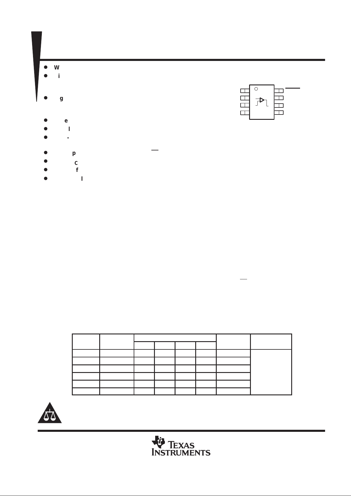
1
2
3
4
8
7
6
5
NULL
IN–
IN+
GND
SHDN
V
DD
OUT
NULL
TLC080
D, DGN OR P PACKAGE
(TOP VIEW)
PowerPAD is a trademark of Texas Instruments Incorporated.
TLC080, TLC081, TLC082, TLC083, TLC084, TLC085, TLC08xA
FAMILY OF WIDE-BANDWIDTH HIGH-OUTPUT-DRIVE SINGLE SUPPLY
OPERATIONAL AMPLIFIERS
SLOS254B – JUNE 1999 – REVISED NOVEMBER 1999
2
POST OFFICE BOX 655303 • DALLAS, TEXAS 75265
TLC080 and TLC081 AVAILABLE OPTIONS
PACKAGED DEVICES PACKAGED DEVICES
T
A
SMALL OUTLINE SMALL OUTLINE
PLASTIC DIP
(D)
†
(DGN)
†
SYMBOL
(P)
0°C to 70°C
TLC080CD
TLC081CD
TLC080CDGN
TLC081CDGN
xxTIACW
xxTIACY
TLC080CP
TLC081CP
°
°
TLC080ID
TLC081ID
TLC080IDGN
TLC081IDGN
xxTIACX
xxTIACZ
TLC080IP
TLC081IP
–
40°C to 125°C
TLC080AID
TLC081AID
—
—
—
—
TLC080AIP
TLC081AIP
†
This package is available taped and reeled. To order this packaging option, add an R suffix to the part number (e.g., TLC080CDR).
‡
Chip forms are tested at TA = 25°C only.
TLC082 and TLC083 AVAILABLE OPTIONS
PACKAGED DEVICES
T
A
SMALL
MSOP
PLASTIC
PLASTIC
OUTLINE
(D)
†
(DGN)
†
SYMBOL
§
(DGQ)
†
SYMBOL
§
DIP
(N)
DIP
(P)
0°C to 70°C
TLC082CD
TLC083CD
TLC082CDGN—xxTIADZ
—
—
TLC083CDGQ—xxTIAEB—TLC083CN
TLC082CP
—
°
°
TLC082ID
TLC083ID
TLC082IDGN—xxTIAEA
—
—
TLC083IDGQ—xxTIAEC—TLC083IN
TLC082IP
—
–
40°C to 125°C
TLC082AID
TLC083AID
—
—
—
—
—
—
—
—
—
TLC083AIN
TLC082AIP
—
†
This package is available taped and reeled. To order this packaging option, add an R suffix to the part number (e.g., TLC082CDR).
‡
Chip forms are tested at TA = 25°C only.
§
xx represents the device date code.
TLC084 and TLC085 AVAILABLE OPTIONS
PACKAGED DEVICES
T
A
SMALL OUTLINE
(D)
†
PLASTIC DIP
(N)
TSSOP
(PWP)
†
0°C to 70°C
TLC084CD
TLC085CD
TLC084CN
TLC085CN
TLC084CPWP
TLC085CPWP
°
°
TLC084ID
TLC085ID
TLC084IN
TLC085IN
TLC084IPWP
TLC085IPWP
–
40°C to 125°C
TLC084AID
TLC085AID
TLC084AIN
TLC085AIN
TLC084AIPWP
TLC085AIPWP
†
This package is available taped and reeled. To order this packaging option, add an R suffix to the part number (e.g.,
TLC084CDR).
‡
Chip forms are tested at TA = 25°C only.
TLC080, TLC081, TLC082, TLC083, TLC084, TLC085, TLC08xA
FAMILY OF WIDE-BANDWIDTH HIGH-OUTPUT-DRIVE SINGLE SUPPLY
OPERATIONAL AMPLIFIERS
SLOS254B – JUNE 1999 – REVISED NOVEMBER 1999
3
POST OFFICE BOX 655303 • DALLAS, TEXAS 75265
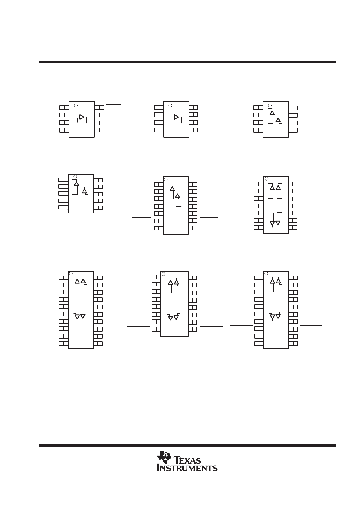
TLC08x P ACKAGE PINOUTS
NC – No internal connection
1
2
3
4
8
7
6
5
NULL
IN–
IN+
GND
SHDN
V
DD
OUT
NULL
TLC080
D, DGN OR P PACKAGE
(TOP VIEW)
1
2
3
4
8
7
6
5
NULL
IN–
IN+
GND
NC
V
DD
OUT
NULL
TLC081
D, DGN OR P PACKAGE
(TOP VIEW)
1
2
3
4
5
6
7
14
13
12
11
10
9
8
1OUT
1IN–
1IN+
GND
NC
1SHDN
NC
V
DD
2OUT
2IN–
2IN+
NC
2SHDN
NC
(TOP VIEW)
1
2
3
4
8
7
6
5
1OUT
1IN–
1IN+
GND
V
DD
2OUT
2IN–
2IN+
TLC082
D, DGN, OR P PACKAGE
(TOP VIEW)
TLC083
D OR N PACKAGE
1
2
3
4
5
6
7
8
16
15
14
13
12
11
10
9
1OUT
1IN–
1IN+
V
DD
2IN+
2IN–
2OUT
1/2SHDN
4OUT
4IN–
4IN+
GND
3IN+
3IN–
3OUT
3/4SHDN
(TOP VIEW)
TLC085
D OR N PACKAGE
1
2
3
4
5
6
7
14
13
12
11
10
9
8
1OUT
1IN–
1IN+
V
DD
2IN+
2IN–
2OUT
4OUT
4IN–
4IN+
GND
3IN+
3IN–
3OUT
(TOP VIEW)
TLC084
D OR N PACKAGE
1
2
3
4
5
10
9
8
7
6
1OUT
1IN–
1IN+
GND
SHDN
V
DD
2OUT
2IN–
2IN+
2SHDN
TLC083
DGQ PACKAGE
(TOP VIEW)
1
2
3
4
5
6
7
8
9
10
20
19
18
17
16
15
14
13
12
11
(TOP VIEW)
TLC084
PWP PACKAGE
1OUT
1IN–
1IN+
VDD
2IN+
2IN–
2OUT
NC
NC
NC
4OUT
4IN–
4IN+
GND
3IN+
3IN–
3OUT
NC
NC
NC
1
2
3
4
5
6
7
8
9
10
20
19
18
17
16
15
14
13
12
11
1OUT
1IN–
1IN+
VDD
2IN+
2IN–
2OUT
1/2SHDN
NC
NC
4OUT
4IN–
4IN+
GND
3IN+
3IN–
3OUT
3/4SHDN
NC
NC
(TOP VIEW)
TLC085
PWP PACKAGE
TLC080, TLC081, TLC082, TLC083, TLC084, TLC085, TLC08xA
FAMILY OF WIDE-BANDWIDTH HIGH-OUTPUT-DRIVE SINGLE SUPPLY
OPERATIONAL AMPLIFIERS
SLOS254B – JUNE 1999 – REVISED NOVEMBER 1999
4
POST OFFICE BOX 655303 • DALLAS, TEXAS 75265
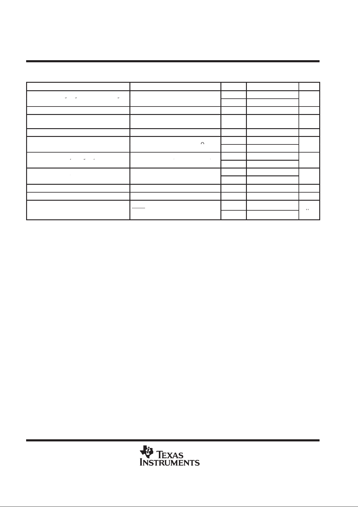
absolute maximum ratings over operating free-air temperature range (unless otherwise noted)
†
Supply voltage, VDD (see Note 1) 17 V. . . . . . . . . . . . . . . . . . . . . . . . . . . . . . . . . . . . . . . . . . . . . . . . . . . . . . . . . . . .
Differential input voltage, VID ±V
DD
. . . . . . . . . . . . . . . . . . . . . . . . . . . . . . . . . . . . . . . . . . . . . . . . . . . . . . . . . . . . . .
Continuous total power dissipation See Dissipation Rating Table. . . . . . . . . . . . . . . . . . . . . . . . . . . . . . . . . . . . .
Operating free-air temperature range, T
A
: C suffix 0°C to 70°C. . . . . . . . . . . . . . . . . . . . . . . . . . . . . . . . . . . . . .
I suffix –40°C to 125°C. . . . . . . . . . . . . . . . . . . . . . . . . . . . . . . . . . . .
Maximum junction temperature, TJ 150°C. . . . . . . . . . . . . . . . . . . . . . . . . . . . . . . . . . . . . . . . . . . . . . . . . . . . . . . . .
Storage temperature range, T
stg
–65°C to 150°C. . . . . . . . . . . . . . . . . . . . . . . . . . . . . . . . . . . . . . . . . . . . . . . . . . .
Lead temperature 1,6 mm (1/16 inch) from case for 10 seconds 260°C. . . . . . . . . . . . . . . . . . . . . . . . . . . . . . .
†
Stresses beyond those listed under “absolute maximum ratings” may cause permanent damage to the device. These are stress ratings only, and
functional operation of the device at these or any other conditions beyond those indicated under “recommended operating conditions” is not
implied. Exposure to absolute-maximum-rated conditions for extended periods may affect device reliability.
NOTE: All voltage values, except differential voltages, are with respect to GND.
DISSIPATION RATING TABLE
PACKAGE
θ
JC
(°C/W)
θ
JA
(°C/W)
TA ≤ 25°C
POWER RATING
D (8) 38.3 176 710 mW
D (14) 26.9 122.3 1022 mW
D (16) 25.7 114.7 1090 mW
DGN (8) 4.7 52.7 2.37 W
DGQ (10) 4.7 52.3 2.39 W
N (14, 16) 32 78 1600 mW
P (8) 41 104 1200 mW
PWP (20) 1.40 26.1 4.79 W
recommended operating conditions
MIN MAX UNIT
pp
Single supply 4.5 16
Suppl
y v
oltage, V
DD
Split supply ±2.25 ±8
V
Common-mode input voltage range, V
ICR
GND VDD–1 V
p
p
C-suffix 0 70
°
Operating free-air temperature, T
A
I-suffix
–40 125
°C
TLC080, TLC081, TLC082, TLC083, TLC084, TLC085, TLC08xA
FAMILY OF WIDE-BANDWIDTH HIGH-OUTPUT-DRIVE SINGLE SUPPLY
OPERATIONAL AMPLIFIERS
SLOS254B – JUNE 1999 – REVISED NOVEMBER 1999
5
POST OFFICE BOX 655303 • DALLAS, TEXAS 75265
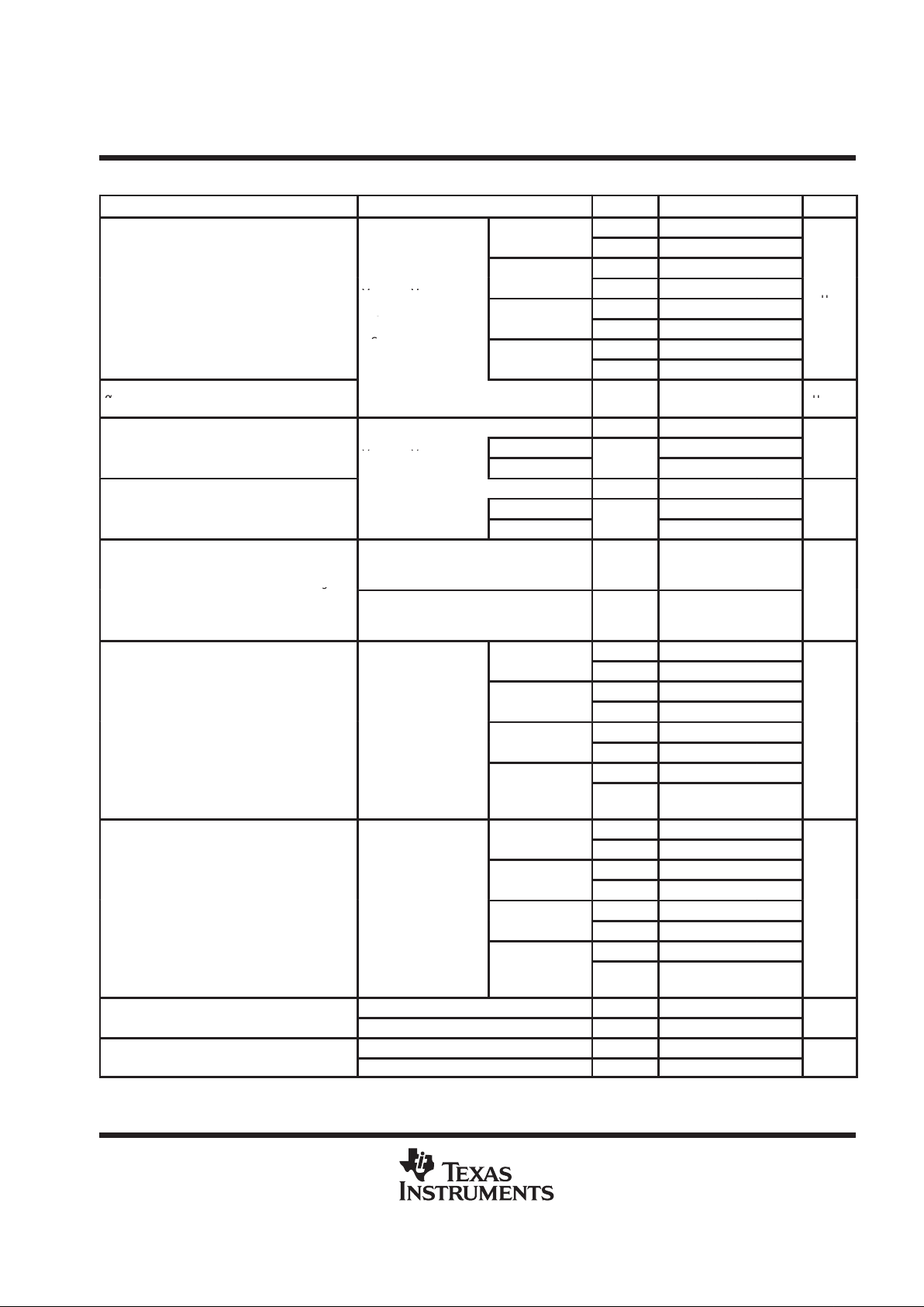
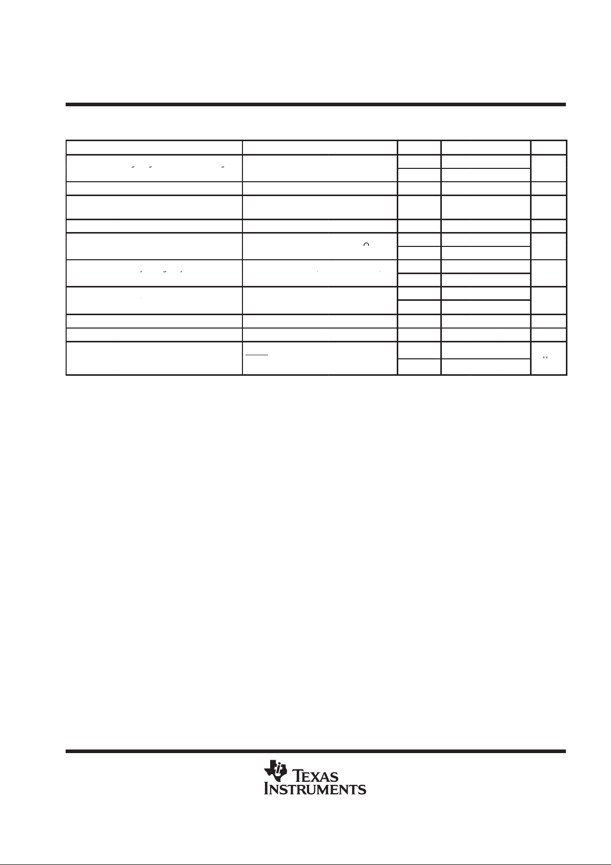
electrical characteristics at specified free-air temperature, VDD = 5 V (unless otherwise noted)
PARAMETER TEST CONDITIONS
T
A
†
MIN TYP MAX
UNIT
25°C 60 1000
TLC080/1/2/3
Full range 1500
25°C 20 750
p
=
TLC080/1/2/3A
Full range 1000
VIOInput offset voltage
V
DD
= 5 V,
VIC = 2.5,
25°C 390 1900
µ
V
IC
VO = 2.5,
TLC084/5
Full range 3000
R
S
= 50
Ω
25°C 390 1400
TLC084/5A
Full range 2000
Temperature coefficient of input
°
α
VIO
offset voltage
1.2µV/°C
25°C 1.9 50
I
IO
Input offset current
TLC08XC
100
pA
V
DD
= 5 V,
VIC = 2.5,
TLC08XI
Full range
700
IC
,
VO = 2.5,
25°C 3 50
I
IB
Input bias current
R
S
=
50 Ω
TLC08XC
100
pA
TLC08XI
Full range
700
Common-mode input voltage
CMRR > 70 dB, RS = 50 Ω 25°C
0
to
3.5
V
ICR
g
range
CMRR > 52 dB,
RS = 50 Ω Full range
0
to
3.5
V
25°C 4.1 4.3
I
OH
= –
1 mA
Full range 3.9
25°C 3.7 4
I
OH
= –20
mA
Full range 3.5
V
OH
High-level output voltage VIC = 2.5 V
25°C 3.4 3.8
V
I
OH
= –35
mA
Full range 3.2
25°C 3.2 3.6
IOH = –50 mA
–40°C to
85°C
3
25°C 0.18 0.25
I
OL
=
1 mA
Full range 0.35
25°C 0.35 0.39
I
OL
= 20
mA
Full range 0.45
V
OL
Low-level output voltage VIC = 2.5 V
25°C 0.43 0.55
V
I
OL
= 35
mA
Full range 0.7
25°C 0.45 0.63
IOL = 50 mA
–40°C to
85°C
0.7
p
Sourcing 25°C 100
IOSShort-circuit output current
Sinking 25°C 100
mA
p
VOH = 1.5 V from positive rail 25°C 57
IOOutput current
VOL = 0.5 V from negative rail 25°C 55
mA
†
Full range is 0°C to 70°C for C suffix and –40°C to 125°C for I suffix. If not specified, full range is –40°C to 125°C.
TLC080, TLC081, TLC082, TLC083, TLC084, TLC085, TLC08xA
FAMILY OF WIDE-BANDWIDTH HIGH-OUTPUT-DRIVE SINGLE SUPPLY
OPERATIONAL AMPLIFIERS
SLOS254B – JUNE 1999 – REVISED NOVEMBER 1999
6
POST OFFICE BOX 655303 • DALLAS, TEXAS 75265
electrical characteristics at specified free-air temperature, VDD = 5 V (unless otherwise noted)
(continued)
PARAMETER TEST CONDITIONS
T
A
†
MIN TYP MAX
UNIT
Large-signal differential voltage
25°C 100 120
A
VD
gg g
amplification
V
O(PP)
= 3 V,
R
L
= 10
kΩ
Full range 100
dB
r
i(d)
Differential input resistance 25°C 1000
GΩ
C
IC
Common-mode input
capacitance
f = 10 kHz 25°C 22.9 pF
z
o
Closed-loop output impedance f = 10 kHz, AV = 10 25°C 0.25
Ω
25°C 100 140
CMRR
Common-mode rejection ratio
V
IC
= 0 to 3 V,
R
S
=
50 Ω
Full range 100
dB
Supply voltage rejection ratio V
= 4.5 V to 16 V, V
= V
/2,
25°C 95 130
k
SVR
ygj
(∆VDD /∆VIO)
DD
,
No load
IC DD
,
Full range 95
dB
Supply current
25°C 1.8 2.5
I
DD
y
(per channel)
V
O
= 2.5 V,
No load
Full range 3.5
mA
V
(ON)
Turnon voltage level Relative to GND 25°C 1.41 V
V
(OFF)
Turnoff voltage level Relative to GND 25°C 1.4 V
Supply current in shutdown
p
25°C 125 200
I
DD(SHDN)
mode (per channe
l)
(TLC080, TLC083, TLC085)
SHDN
≤ 1.45
V
Full range 250
µ
A
†
Full range is 0°C to 70°C for C suffix and –40°C to 125°C for I suffix. If not specified, full range is –40°C to 125°C.
TLC080, TLC081, TLC082, TLC083, TLC084, TLC085, TLC08xA
FAMILY OF WIDE-BANDWIDTH HIGH-OUTPUT-DRIVE SINGLE SUPPLY
OPERATIONAL AMPLIFIERS
SLOS254B – JUNE 1999 – REVISED NOVEMBER 1999
7
POST OFFICE BOX 655303 • DALLAS, TEXAS 75265
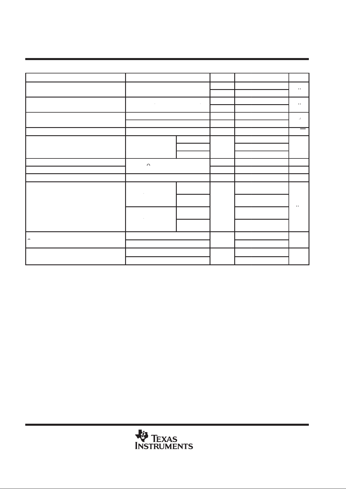
operating characteristics at specified free-air temperature, VDD = 5 V (unless otherwise noted)
PARAMETER TEST CONDITIONS
T
A
†
MIN TYP MAX UNIT
V
= 0.8 V, C
= 50 pF,
25°C
10 16
SR+Positive slew rate at unity gain
O(PP)
,
RL = 10 kΩ
L
,
Full range 9.5
V/µs
V
= 0.8 V, C
= 50 pF,
25°C
12.5 19
SR–Negative slew rate at unity gain
O(PP)
,
RL = 10 kΩ
L
,
Full range 10
V/µs
p
f = 100 Hz 25°C 12
VnEquivalent input noise voltage
f = 1 kHz 25°C 8.5
n
V/√H
z
I
n
Equivalent input noise current f = 1 kHz 25°C 0.6
fA/√Hz
=
AV = 1 0.002%
THD + N Total harmonic distortion plus noise
V
O(PP)
= 3 V,
RL = 10 kΩ and 250 Ω,
AV = 10
25°C
0.012%
f = 1 kHz
AV = 100 0.085%
t
(on)
Amplifier turnon time
‡
25°C 0.15 µs
t
(off)
Amplifier turnoff time
‡
R
L
=
10 kΩ
25°C 1.3 µs
Gain-bandwidth product
f = 10 kHz, RL = 10 kΩ
25°C 10 MHz
V
(STEP)PP
= 1 V,
A
= –1,
0.1% 0.18
V
,
CL = 10 pF,
RL = 10 kΩ
0.01%
°
0.39
tsSettling time
V
(STEP)PP
= 1 V,
A
= –1,
0.1%
25°C
0.18
µ
s
V
,
CL = 47 pF,
RL = 10 kΩ
0.01% 0.39
RL = 10 kΩ, CL = 50 pF
°
32°
φmPhase margin
RL = 10 kΩ, CL = 0 pF
25°C
40°
RL = 10 kΩ, CL = 50 pF
°
2.2
Gain margin
RL = 10 kΩ, CL = 0 pF
25°C
3.3
dB
†
Full range is 0°C to 70°C for C suffix and –40°C to 125°C for I suffix. If not specified, full range is –40°C to 125°C.
‡
Disable time and enable time are defined as the interval between application of the logic signal to SHDN and the point at which the supply current
has reached half its final value.
TLC080, TLC081, TLC082, TLC083, TLC084, TLC085, TLC08xA
FAMILY OF WIDE-BANDWIDTH HIGH-OUTPUT-DRIVE SINGLE SUPPLY
OPERATIONAL AMPLIFIERS
SLOS254B – JUNE 1999 – REVISED NOVEMBER 1999
8
POST OFFICE BOX 655303 • DALLAS, TEXAS 75265
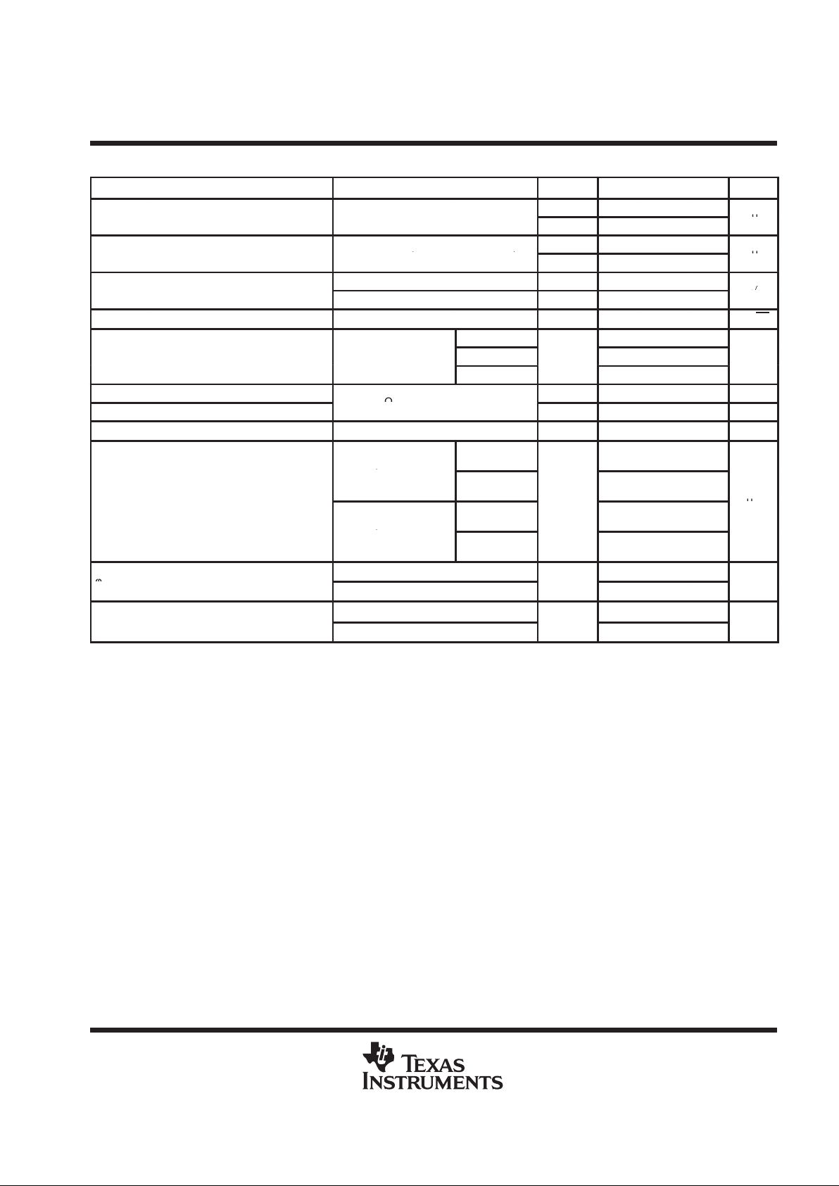
electrical characteristics at specified free-air temperature, VDD = 12 V (unless otherwise noted)
PARAMETER TEST CONDITIONS
T
A
†
MIN TYP MAX
UNIT
25°C 60 1000
TLC080/1/2/3
Full range 1500
25°C 20 750
p
=
TLC080/1/2/3A
Full range 1000
VIOInput offset voltage
V
DD
= 12
V
VIC = 6,
25°C 390 1900
µ
V
IC
VO = 6,
TLC084/5
Full range 3000
R
S
= 50
Ω
25°C 390 1400
TLC084/5A
Full range 2000
Temperature coefficient of input
°
α
VIO
offset voltage
1.2µV/°C
25°C 1.5 50
I
IO
Input offset current
TLC08xC
100
pA
V
DD
= 12
V
VIC = 6,
TLC08xI
Full range
700
IC
,
VO = 6,
25°C 2 50
I
IB
Input bias current
R
S
=
50 Ω
TLC08xC
100
pA
TLC08xI
Full range
700
Common-mode input voltage
CMRR > 70 dB RS = 50 Ω 25°C
0
to
10.5
V
ICR
g
range
CMRR > 52 dB
RS = 50 Ω Full range
0
to
10.5
V
25°C 11.1 11.2
I
OH
= –
1 mA
Full range 11
25°C 10.8 11
I
OH
= –20
mA
Full range 10.7
V
OH
High-level output voltage VIC = 6 V
25°C 10.6 10.7
V
I
OH
= –35
mA
Full range 10.3
25°C 10.3 10.5
IOH = –50 mA
–40°C to
85°C
10.2
25°C 0.17 0.25
I
OL
=
1 mA
Full range 0.35
25°C 0.35 0.45
I
OL
= 20
mA
Full range 0.5
V
OL
Low-level output voltage VIC = 6 V
25°C 0.4 0.52
V
I
OL
= 35
mA
Full range 0.6
25°C 0.45 0.6
IOL = 50 mA
–40°C to
85°C
0.65
p
Sourcing 25°C 150
IOSShort-circuit output current
Sinking 25°C 150
mA
p
VOH = 1.5 V from positive rail 25°C 57
IOOutput current
VOL = 0.5 V from negative rail 25°C 55
mA
†
Full range is 0°C to 70°C for C suffix and –40°C to 125°C for I suffix. If not specified, full range is –40°C to 125°C.
TLC080, TLC081, TLC082, TLC083, TLC084, TLC085, TLC08xA
FAMILY OF WIDE-BANDWIDTH HIGH-OUTPUT-DRIVE SINGLE SUPPLY
OPERATIONAL AMPLIFIERS
SLOS254B – JUNE 1999 – REVISED NOVEMBER 1999
9
POST OFFICE BOX 655303 • DALLAS, TEXAS 75265
electrical characteristics at specified free-air temperature, VDD = 12 V (unless otherwise noted)
(continued)
PARAMETER TEST CONDITIONS
T
A
†
MIN TYP MAX
UNIT
Large-signal differential voltage
25°C 120 140
A
VD
gg g
amplification
V
O(PP)
= 8 V,
R
L
= 10
kΩ
Full range 120
dB
r
i(d)
Differential input resistance 25°C 1000
GΩ
C
IC
Common-mode input
capacitance
f = 10 kHz 25°C 21.6 pF
z
o
Closed-loop output impedance f = 10 kHz, AV = 10 25°C 0.25
Ω
25°C 100 140
CMRR
Common-mode rejection ratio
V
IC
= 0 to 10 V,
R
S
=
50 Ω
Full range 100
dB
Supply voltage rejection ratio V
= 4.5 V to 16 V, V
= V
/2,
25°C 95 130
k
SVR
ygj
(∆VDD /∆VIO)
DD
,
No load
IC DD
,
Full range 95
dB
Supply current
25°C 1.9 2.9
I
DD
y
(per channel)
V
O
= 7.5 V,
No load
Full range 3.5
mA
V
(ON)
Turnon voltage level Relative to GND 25°C 1.39 V
V
(OFF)
Turnoff voltage level Relative to GND 25°C 1.38 V
Supply current in shutdown
25°C 125 200
I
DD(SHDN)
mode
(TLC080, TLC083
,
TLC085) (per channel)
SHDN
≤ 1.45
V
Full range 250
µ
A
†
Full range is 0°C to 70°C for C suffix and –40°C to 125°C for I suffix. If not specified, full range is –40°C to 125°C.
TLC080, TLC081, TLC082, TLC083, TLC084, TLC085, TLC08xA
FAMILY OF WIDE-BANDWIDTH HIGH-OUTPUT-DRIVE SINGLE SUPPLY
OPERATIONAL AMPLIFIERS
SLOS254B – JUNE 1999 – REVISED NOVEMBER 1999
10
POST OFFICE BOX 655303 • DALLAS, TEXAS 75265
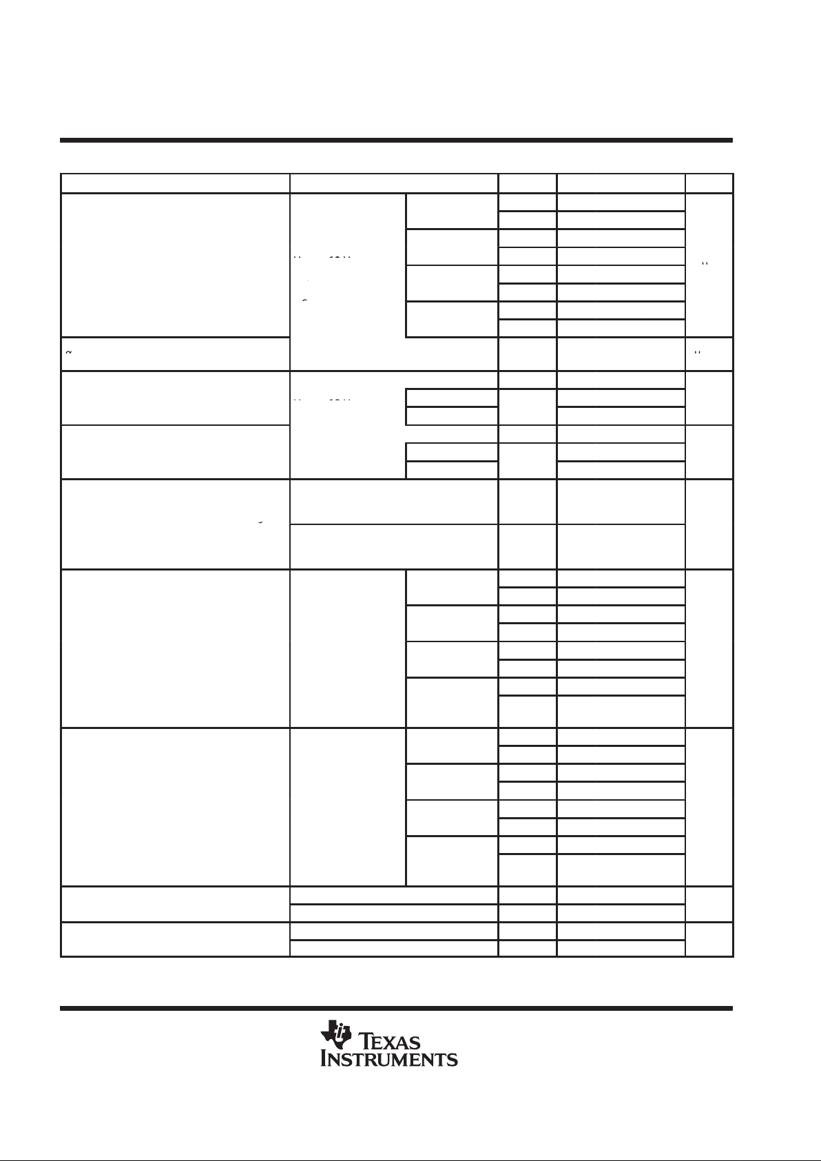
operating characteristics at specified free-air temperature, VDD = 12 V (unless otherwise noted)
PARAMETER TEST CONDITIONS
T
A
†
MIN TYP MAX UNIT
V
= 2 V, C
= 50 pF,
25°C
10 16
SR+Positive slew rate at unity gain
O(PP)
,
RL = 10 kΩ
L
,
Full range 9.5
V/µs
V
= 2 V, C
= 50 pF,
25°C
12.5 19
SR–Negative slew rate at unity gain
O(PP)
,
RL = 10 kΩ
L
,
Full range 10
V/µs
p
f = 100 Hz 25°C 14
VnEquivalent input noise voltage
f = 1 kHz 25°C 8.5
n
V/√H
z
I
n
Equivalent input noise current f = 1 kHz 25°C 0.6
fA/√Hz
=
AV = 1 0.002%
THD + N Total harmonic distortion plus noise
V
O(PP)
= 8 V,
RL = 10 kΩ and 250 Ω,
AV = 10
25°C
0.005%
f = 1 kHz
AV = 100 0.022%
t
(on)
Amplifier turnon time
‡
25°C 0.47 µs
t
(off)
Amplifier turnoff time
‡
R
L
=
10 kΩ
25°C 2.5 µs
Gain-bandwidth product
f = 10 kHz, RL = 10 kΩ
25°C 10 MHz
V
(STEP)PP
= 1 V,
A
= –1,
0.1% 0.17
V
,
CL = 10 pF,
RL = 10 kΩ
0.01%
°
0.22
tsSettling time
V
(STEP)PP
= 1 V,
A
= –1,
0.1%
25°C
0.17
µ
s
V
,
CL = 47 pF,
RL = 10 kΩ
0.01% 0.29
RL = 10 kΩ, CL = 50 pF
°
37°
φmPhase margin
RL = 10 kΩ, CL = 0 pF
25°C
42°
RL = 10 kΩ, CL = 50 pF
°
3.1
Gain margin
RL = 10 kΩ, CL = 0 pF
25°C4dB
†
Full range is 0°C to 70°C for C suffix and –40°C to 125°C for I suffix. If not specified, full range is –40°C to 125°C.
‡
Disable time and enable time are defined as the interval between application of the logic signal to SHDN and the point at which the supply current
has reached half its final value.
 Loading...