


Texas Instruments TLC5615IP, TLC5615IDR, TLC5615ID, TLC5615CP, TLC5615CDR Datasheet
...
|
|
|
|
|
|
|
|
TLC5615C, TLC5615I |
||||
|
|
10-BIT DIGITAL-TO-ANALOG CONVERTERS |
||||||||||
|
|
|
SLAS142C ± OCTOBER 1996 ± REVISED MARCH 2000 |
|||||||||
|
|
|
|
|
|
|
|
|
|
|
||
D |
10-Bit CMOS Voltage Output DAC in an |
applications |
|
|
|
|
|
|||||
|
8-Terminal Package |
D Battery-Powered Test Instruments |
||||||||||
D 5-V Single Supply Operation |
||||||||||||
D Digital Offset and Gain Adjustment |
||||||||||||
D 3-Wire Serial Interface |
||||||||||||
D |
Battery Operated/Remote Industrial |
|||||||||||
D High-Impedance Reference Inputs |
||||||||||||
|
Controls |
|
|
|
|
|
||||||
|
|
|
|
|
|
|
|
|||||
D Voltage Output Range . . . 2 Times the |
D Machine and Motion Control Devices |
|||||||||||
|
Reference Input Voltage |
|||||||||||
|
D |
Cellular Telephones |
|
|
|
|
||||||
D Internal Power-On Reset |
|
|
|
|
||||||||
|
|
|
|
|
|
|
|
|
|
|||
D Low Power Consumption . . . 1.75 mW Max |
|
D, P, OR DGK PACKAGE |
||||||||||
D Update Rate of 1.21 MHz |
|
|
|
|
|
(TOP VIEW) |
|
|
||||
|
|
|
|
|
|
|
|
|
|
|||
D Settling Time to 0.5 LSB . . . 12.5 s Typ |
|
DIN |
|
1 |
8 |
|
VDD |
|||||
|
|
|
||||||||||
D |
Monotonic Over Temperature |
|
SCLK |
|
2 |
7 |
|
OUT |
||||
|
|
|
|
|
|
|
|
|
|
REFIN |
||
D Pin Compatible With the Maxim MAX515 |
|
|
CS |
|
|
3 |
6 |
|
||||
|
|
|
DOUT |
|
4 |
5 |
|
AGND |
||||
description
The TLC5615 is a 10-bit voltage output digital-to-analog converter (DAC) with a buffered reference input (high impedance). The DAC has an output voltage range that is two times the reference voltage, and the DAC is monotonic. The device is simple to use, running from a single supply of 5 V. A power-on-reset function is incorporated to ensure repeatable start-up conditions.
Digital control of the TLC5615 is over a three-wire serial bus that is CMOS compatible and easily interfaced to industry standard microprocessor and microcontroller devices. The device receives a 16-bit data word to produce the analog output. The digital inputs feature Schmitt triggers for high noise immunity. Digital communication protocols include the SPI , QSPI , and Microwire standards.
The 8-terminal small-outline D package allows digital control of analog functions in space-critical applications. The TLC5615C is characterized for operation from 0°C to 70°C. The TLC5615I is characterized for operation from ±40°C to 85°C.
AVAILABLE OPTIONS
PACKAGE
TA |
SMALL OUTLINE² |
PLASTIC SMALL OUTLINE |
PLASTIC DIP |
|
(D) |
(DGK) |
(P) |
||
|
||||
|
|
|
|
|
0°C to 70°C |
TLC5615CD |
TLC5615CDGK |
TLC5615CP |
|
|
|
|
|
|
± 40°C to 85°C |
TLC5615ID |
TLC5615IDGK |
TLC5615IP |
² Available in tape and reel as the TLC5615CDR and the TLC5615IDR
Please be aware that an important notice concerning availability, standard warranty, and use in critical applications of Texas Instruments semiconductor products and disclaimers thereto appears at the end of this data sheet.
SPI and QSPI are trademarks of Motorola, Inc.
Microwire is a trademark of National Semiconductor Corporation.
PRODUCTION DATA information is current as of publication date. Products conform to specifications per the terms of Texas Instruments standard warranty. Production processing does not necessarily include testing of all parameters.
Copyright 2000, Texas Instruments Incorporated
POST OFFICE BOX 655303 •DALLAS, TEXAS 75265 |
1 |
TLC5615C, TLC5615I
10-BIT DIGITAL-TO-ANALOG CONVERTERS
SLAS142C ± OCTOBER 1996 ± REVISED MARCH 2000
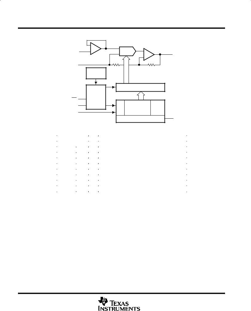
functional block diagram
|
_ |
|
|
|
|
REFIN |
+ |
DAC |
+ |
2 |
OUT |
|
_ |
||||
|
|
|
(Voltage Output)
AGND
R R
Power-ON
Reset
|
|
10-Bit DAC Register |
|
||
|
Control |
|
|
|
|
CS |
Logic |
|
|
|
|
2 |
(LSB) |
(MSB) |
4 |
|
|
SCLK |
|
||||
0s |
10 Data Bits |
Dummy |
|
||
DIN |
|
Bits |
|
||
|
|
|
|
|
|
|
|
16-Bit Shift Register |
DOUT |
||
|
|
|
|
|
Terminal Functions |
|
|
|
|
|
|
|
|
TERMINAL |
I/O |
DESCRIPTION |
|
|
NAME |
NO. |
|||
|
|
|
|||
|
|
|
|
|
|
|
DIN |
1 |
I |
Serial data input |
|
|
|
|
|
|
|
|
SCLK |
2 |
I |
Serial clock input |
|
|
|
|
|
|
|
|
|
|
3 |
I |
Chip select, active low |
|
CS |
|
|||
|
|
|
|
|
|
|
DOUT |
4 |
O |
Serial data output for daisy chaining |
|
|
|
|
|
|
|
|
AGND |
5 |
|
Analog ground |
|
|
|
|
|
|
|
|
REFIN |
6 |
I |
Reference input |
|
|
|
|
|
|
|
|
OUT |
7 |
O |
DAC analog voltage output |
|
|
|
|
|
|
|
|
VDD |
8 |
|
Positive power supply |
|
absolute maximum ratings over operating free-air temperature range (unless otherwise noted)²
Supply voltage (VDD to AGND) . . . . . . . . . . . . . . . . . . . . . . . . . . . . . . . . . . . . . . . . . . . . . . |
. . . . . . . . . . . . . . . . . 7 |
V |
Digital input voltage range to AGND . . . . . . . . . . . . . . . . . . . . . . . . . . . . . . . . . . . . . . . . . . |
± 0.3 V to VDD + 0.3 |
V |
Reference input voltage range to AGND . . . . . . . . . . . . . . . . . . . . . . . . . . . . . . . . . . . . . . |
± 0.3 V to VDD + 0.3 |
V |
Output voltage at OUT from external source . . . . . . . . . . . . . . . . . . . . . . . . . . . . . . . . . . . . |
. . . . . . . . VDD + 0.3 |
V |
Continuous current at any terminal . . . . . . . . . . . . . . . . . . . . . . . . . . . . . . . . . . . . . . . . . . . . |
. . . . . . . . . . . . ± 20 mA |
|
Operating free-air temperature range, TA: TLC5615C . . . . . . . . . . . . . . . . . . . . . . . . . . . . |
. . . . . . . . 0°C to 70°C |
|
TLC5615I . . . . . . . . . . . . . . . . . . . . . . . . . . . . . |
. . . . . . ±40°C to 85°C |
|
Storage temperature range, Tstg . . . . . . . . . . . . . . . . . . . . . . . . . . . . . . . . . . . . . . . . . . . . . . |
. . . . . ±65°C to 150°C |
|
Lead temperature 1,6 mm (1/16 inch) from case for 10 seconds . . . . . . . . . . . . . . . . . . |
. . . . . . . . . . . . . 260°C |
|
²Stresses beyond those listed under ªabsolute maximum ratingsº may cause permanent damage to the device. These are stress ratings only, and functional operation of the device at these or any other conditions beyond those indicated under ªrecommended operating conditionsº is not implied. Exposure to absolute-maximum-rated conditions for extended periods may affect device reliability.
2 |
POST OFFICE BOX 655303 •DALLAS, TEXAS 75265 |
TLC5615C, TLC5615I 10-BIT DIGITAL-TO-ANALOG CONVERTERS
SLAS142C ± OCTOBER 1996 ± REVISED MARCH 2000
recommended operating conditions
|
|
MIN |
NOM |
MAX |
UNIT |
|
|
|
|
|
|
Supply voltage, VDD |
|
4.5 |
5 |
5.5 |
V |
High-level digital input voltage, VIH |
|
2.4 |
|
|
V |
Low-level digital input voltage, VIL |
|
|
|
0.8 |
V |
Reference voltage, Vref to REFIN terminal |
|
2 |
2.048 |
VDD ± 2 |
V |
Load resistance, RL |
|
2 |
|
|
kΩ |
Operating free-air temperature, TA |
TLC5615C |
0 |
|
70 |
°C |
TLC5615I |
± 40 |
|
85 |
°C |
|
|
|
||||
|
|
|
|
|
|
electrical characteristics over recommended operating free-air temperature range, VDD = 5 V ± 5%,
Vref = 2.048 V (unless otherwise noted)
static DAC specifications
|
PARAMETER |
TEST CONDITIONS |
MIN |
TYP |
MAX |
UNIT |
||
|
|
|
|
|
|
|
|
|
|
Resolution |
|
|
10 |
|
|
bits |
|
|
|
|
|
|
|
|
|
|
|
Integral nonlinearity, end point adjusted (INL) |
Vref = 2.048 V, |
See Note 1 |
|
|
± 1 |
LSB |
|
|
Differential nonlinearity (DNL) |
Vref = 2.048 V, |
See Note 2 |
|
± 0.1 |
± 0.5 |
LSB |
|
EZS |
Zero-scale error (offset error at zero scale) |
Vref = 2.048 V, |
See Note 3 |
|
|
± 3 |
LSB |
|
|
Zero-scale-error temperature coefficient |
Vref = 2.048 V, |
See Note 4 |
|
3 |
|
ppm/°C |
|
EG |
Gain error |
Vref = 2.048 V, |
See Note 5 |
|
|
± 3 |
LSB |
|
|
Gain-error temperature coefficient |
Vref = 2.048 V, |
See Note 6 |
|
1 |
|
ppm/°C |
|
PSRR |
Power-supply rejection ratio |
Zero scale |
See Notes 7 and 8 |
80 |
|
|
dB |
|
|
|
|
|
|||||
Gain |
80 |
|
|
|||||
|
|
|
|
|
|
|
||
|
|
|
|
|
|
|
|
|
|
Analog full scale output |
RL = 100 kΩ |
|
|
2Vref(1023/1024) |
|
V |
|
NOTES: 1. The relative accuracy or integral nonlinearity (INL), sometimes referred to as linearity error, is the maximum deviation of the output from the line between zero and full scale excluding the effects of zero code and full-scale errors (see text).
2.The differential nonlinearity (DNL), sometimes referred to as differential error, is the difference between the measured and ideal 1 LSB amplitude change of any two adjacent codes. Monotonic means the output voltage changes in the same direction (or remains constant) as a change in the digital input code.
3.Zero-scale error is the deviation from zero-voltage output when the digital input code is zero (see text).
4.Zero-scale-error temperature coefficient is given by: EZS TC = [EZS (Tmax) ± EZS (Tmin)]/Vref × 106/(Tmax ± Tmin).
5.Gain error is the deviation from the ideal output (Vref ± 1 LSB) with an output load of 10 kΩ excluding the effects of the zero-scale error.
6.Gain temperature coefficient is given by: EG TC = [EG(Tmax) ± EG (Tmin)]/Vref × 106/(Tmax ± Tmin).
7.Zero-scale-error rejection ratio (EZS-RR) is measured by varying the VDD from 4.5 V to 5.5 V dc and measuring the proportion of this signal imposed on the zero-code output voltage.
8.Gain-error rejection ratio (EG-RR) is measured by varying the VDD from 4.5 V to 5.5 V dc and measuring the proportion of this signal imposed on the full-scale output voltage after subtracting the zero-scale change.
voltage output (OUT)
|
PARAMETER |
TEST CONDITIONS |
MIN |
TYP |
MAX |
UNIT |
|
|
|
|
|
|
|
|
|
VO |
Voltage output range |
RL = 10 kΩ |
|
0 |
|
VDD±0.4 |
V |
|
Output load regulation accuracy |
VO(OUT) = 2 V, |
RL = 2 kΩ |
|
|
0.5 |
LSB |
IOSC |
Output short circuit current |
OUT to VDD or AGND |
|
20 |
|
mA |
|
VOL(low) |
Output voltage, low-level |
IO(OUT) ≤ 5 mA |
|
|
|
0.25 |
V |
VOH(high) |
Output voltage, high-level |
IO(OUT) ≤ ±5 mA |
|
4.75 |
|
|
V |
POST OFFICE BOX 655303 •DALLAS, TEXAS 75265 |
3 |
TLC5615C, TLC5615I
10-BIT DIGITAL-TO-ANALOG CONVERTERS
SLAS142C ± OCTOBER 1996 ± REVISED MARCH 2000
electrical characteristics over recommended operating free-air temperature range, VDD = 5 V ± 5%,
Vref = 2.048 V (unless otherwise noted) (continued)
reference input (REFIN)
|
PARAMETER |
TEST CONDITIONS |
MIN TYP |
MAX |
UNIT |
|
|
|
|
|
|
VI |
Input voltage |
|
0 |
VDD± 2 |
V |
ri |
Input resistance |
|
10 |
|
MΩ |
Ci |
Input capacitance |
|
5 |
|
pF |
digital inputs (DIN, SCLK, CS)
|
PARAMETER |
|
TEST CONDITIONS |
MIN TYP MAX |
UNIT |
|
|
|
|
|
|
VIH |
High-level digital input voltage |
|
|
2.4 |
V |
VIL |
Low-level digital input voltage |
|
|
0.8 |
V |
IIH |
High-level digital input current |
VI = VDD |
|
± 1 |
µA |
IIL |
Low-level digital input current |
VI = 0 |
|
± 1 |
µA |
Ci |
Input capacitance |
|
|
8 |
pF |
digital output (DOUT)
|
PARAMETER |
|
TEST CONDITIONS |
MIN |
TYP MAX |
UNIT |
|
|
|
|
|
|
|
VOH |
Output voltage, high-level |
IO = ±2 mA |
|
VDD±1 |
|
V |
VOL |
Output voltage, low-level |
IO = 2 mA |
|
|
0.4 |
V |
power supply
|
PARAMETER |
|
TEST CONDITIONS |
MIN |
TYP |
MAX |
UNIT |
|
|
|
|
|
|
|
|
|
|
VDD |
Supply voltage |
|
|
|
4.5 |
5 |
5.5 |
V |
|
|
VDD = 5.5 V, |
|
|
|
|
µA |
|
|
|
No load, |
|
Vref = 0 |
|
150 |
250 |
|
IDD |
Power supply current |
All inputs = 0 V or VDD |
|
|
|
|
|
|
VDD = 5.5 V, |
|
|
|
|
µA |
|||
|
|
|
|
|
|
|||
|
|
No load, |
|
Vref = 2.048 V |
|
230 |
350 |
|
|
|
All inputs = 0 V or VDD |
|
|
|
|
|
|
analog output dynamic performance
PARAMETER |
TEST CONDITIONS |
MIN |
TYP MAX |
UNIT |
|
|
|
|
|
|
Vref = 1 Vpp at 1 kHz + 2.048 Vdc, |
|
|
|
Signal-to-noise + distortion, S/(N+D) |
code = 11 1111 1111, |
60 |
|
dB |
|
See Note 9 |
|
|
|
NOTE 9: The limiting frequency value at 1 Vpp is determined by the output-amplifier slew rate.
4 |
POST OFFICE BOX 655303 •DALLAS, TEXAS 75265 |
TLC5615C, TLC5615I 10-BIT DIGITAL-TO-ANALOG CONVERTERS
SLAS142C ± OCTOBER 1996 ± REVISED MARCH 2000
digital input timing requirements (see Figure 1)
|
|
|
|
|
|
PARAMETER |
MIN NOM MAX |
UNIT |
|
|
|
|
|
|
|
|
|
tsu(DS) |
Setup time, DIN before SCLK high |
45 |
ns |
|||||
th(DH) |
Hold time, DIN valid after SCLK high |
0 |
ns |
|||||
tsu(CSS) |
Setup time, |
|
low to SCLK high |
1 |
ns |
|||
CS |
||||||||
tsu(CS1) |
Setup time, |
|
high to SCLK high |
50 |
ns |
|||
CS |
||||||||
th(CSH0) |
Hold time, SCLK low to |
|
low |
1 |
ns |
|||
CS |
||||||||
th(CSH1) |
Hold time, SCLK low to |
|
|
high |
0 |
ns |
||
CS |
||||||||
tw(CS) |
Pulse duration, minimum chip select pulse width high |
20 |
ns |
|||||
tw(CL) |
Pulse duration, SCLK low |
25 |
ns |
|||||
tw(CH) |
Pulse duration, SCLK high |
25 |
ns |
|||||
output switching characteristic
PARAMETER |
|
TEST CONDITIONS |
MIN NOM MAX |
UNIT |
|
|
|
|
|
tpd(DOUT) Propagation delay time, DOUT |
CL = 50 pF |
|
50 |
ns |
operating characteristics over recommended operating free-air temperature range, VDD = 5 V ± 5%,
Vref = 2.048 V (unless otherwise noted)
analog output dynamic performance
|
PARAMETER |
TEST CONDITIONS |
MIN |
TYP MAX |
UNIT |
|
|
|
|
|
|
|
|
SR |
Output slew rate |
CL = 100 pF, |
RL = 10 kΩ, |
0.3 |
0.5 |
V/µs |
TA = 25°C |
|
|||||
|
|
|
|
|
|
|
ts |
Output settling time |
To 0.5 LSB, |
CL = 100 pF, |
|
12.5 |
µs |
RL = 10 kΩ, |
See Note 10 |
|
||||
|
|
|
|
|
||
|
Glitch energy |
DIN = All 0s to all 1s |
|
|
5 |
nV s |
NOTE 10: Settling time is the time for the output signal to remain within ± 0.5 LSB of the final measured value for a digital input code change of 000 hex to 3FF hex or 3FF hex to 000 hex.
reference input (REFIN)
PARAMETER |
TEST CONDITIONS |
MIN TYP |
MAX |
UNIT |
|
|
|
|
|
|
|
Reference feedthrough |
REFIN = 1 Vpp at 1 kHz + 2.048 Vdc (see Note 11) |
± 80 |
dB |
||
Reference input |
REFIN = 0.2 Vpp + 2.048 Vdc |
REFIN = 0.2 Vpp + 2.048 Vdc |
30 |
|
kHz |
bandwidth (f±3dB) |
|
||||
|
|
|
|
|
|
NOTE 11: Reference feedthrough is measured at the DAC output with an input code = 000 hex and a Vref input = 2.048 Vdc + 1 Vpp at 1 kHz.
POST OFFICE BOX 655303 •DALLAS, TEXAS 75265 |
5 |

TLC5615C, TLC5615I
10-BIT DIGITAL-TO-ANALOG CONVERTERS
SLAS142C ± OCTOBER 1996 ± REVISED MARCH 2000
PARAMETER MEASUREMENT INFORMATION
CS |
|
|
|
|
th(CSH0) |
tsu(CSS) |
|
|
tw(CS) |
|
tw(CH) |
tw(CL) |
th(CSH1) |
tsu(CS1) |
SCLK |
|
|
|
|
See Note A |
|
|
See Note C |
See Note A |
tsu(DS)  th(DH)
DIN
tpd(DOUT)
DOUT |
Previous LSB |
MSB |
LSB |
See Note B
NOTES: A. The input clock, applied at the SCLK terminal, should be inhibited low when CS is high to minimize clock feedthrough.
B.Data input from preceeding conversion cycle.
C.Sixteenth SCLK falling edge
Figure 1. Timing Diagram
6 |
POST OFFICE BOX 655303 •DALLAS, TEXAS 75265 |
 Loading...