


Texas Instruments TLC549IP, TLC549IDR, TLC549ID, TLC549CP, TLC549CDR Datasheet
...TLC548C, TLC548I, TLC549C, TLC549I 8-BIT ANALOG-TO-DIGITAL CONVERTERS WITH SERIAL CONTROL
SLAS067C ± NOVEMBER 1983 ± REVISED SEPTEMBER 1996
D Microprocessor Peripheral or Standalone |
D OR P PACKAGE |
||||||||
Operation |
|
|
|
(TOP VIEW) |
|
|
|||
D 8-Bit Resolution A/D Converter |
REF + |
|
|
|
|
|
VCC |
||
|
1 |
8 |
|
|
|||||
|
|
|
|||||||
D Differential Reference Input Voltages |
|
|
|
||||||
ANALOG IN |
|
|
|
|
|
||||
|
2 |
7 |
|
|
I/O CLOCK |
||||
D Conversion Time . . . 17 μs Max |
REF± |
|
3 |
6 |
|
|
DATA OUT |
||
|
|
|
|||||||
D Total Access and Conversion Cycles Per |
GND |
|
4 |
5 |
|
|
CS |
|
|
|
|
|
|
||||||
|
|
|
|
|
|
|
|
||
Second |
|
|
|
|
|
|
|
|
|
|
|
|
|
|
|
|
|
|
|
± TLC548 . . . |
up to 45 500 |
|
|
|
|
|
|
|
|
± TLC549 . . . |
up to 40 000 |
|
|
|
|
|
|
|
|
DOn-Chip Software-Controllable Sample-and-Hold Function
DTotal Unadjusted Error . . . ± 0.5 LSB Max
D4-MHz Typical Internal System Clock
DWide Supply Range . . . 3 V to 6 V
DLow Power Consumption . . . 15 mW Max
DIdeal for Cost-Effective, High-Performance Applications including Battery-Operated Portable Instrumentation
DPinout and Control Signals Compatible With the TLC540 and TLC545 8-Bit A/D Converters and with the TLC1540 10-Bit A/D Converter
DCMOS Technology
description
The TLC548 and TLC549 are CMOS analog-to-digital converter (ADC) integrated circuits built around an 8-bit switched-capacitor successive-approximation ADC. These devices are designed for serial interface with a microprocessor or peripheral through a 3-state data output and an analog input. The TLC548 and TLC549 use only the input/output clock (I/O CLOCK) input along with the chip select (CS) input for data control. The maximum I/O CLOCK input frequency of the TLC548 is 2.048 MHz, and the I/O CLOCK input frequency of the TLC549 is specified up to 1.1 MHz.
AVAILABLE OPTIONS
|
PACKAGE |
||
TA |
|
|
|
SMALL OUTLINE |
PLASTIC DIP |
||
|
(D) |
(P) |
|
|
|
|
|
0°C to 70°C |
TLC548CD |
TLC548CP |
|
TLC549CD |
TLC549CP |
||
|
|||
|
|
|
|
± 40°C to 85°C |
TLC548ID |
TLC548IP |
|
TLC549ID |
TLC549IP |
||
|
|||
|
|
|
|
Please be aware that an important notice concerning availability, standard warranty, and use in critical applications of
Texas Instruments semiconductor products and disclaimers thereto appears at the end of this data sheet.
PRODUCTION DATA information is current as of publication date. Products conform to specifications per the terms of Texas Instruments standard warranty. Production processing does not necessarily include testing of all parameters.
Copyright 1996, Texas Instruments Incorporated
POST OFFICE BOX 655303 •DALLAS, TEXAS 75265 |
1 |
TLC548C, TLC548I, TLC549C, TLC549I 8-BIT ANALOG-TO-DIGITAL CONVERTERS WITH SERIAL CONTROL
SLAS067C ± NOVEMBER 1983 ± REVISED SEPTEMBER 1996
description (continued)
Operation of the TLC548 and the TLC549 is very similar to that of the more complex TLC540 and TLC541 devices; however, the TLC548 and TLC549 provide an on-chip system clock that operates typically at 4 MHz and requires no external components. The on-chip system clock allows internal device operation to proceed independently of serial input/output data timing and permits manipulation of the TLC548 and TLC549 as desired for a wide range of software and hardware requirements. The I/O CLOCK together with the internal system clock allow high-speed data transfer and conversion rates of 45 500 conversions per second for the TLC548, and 40 000 conversions per second for the TLC549.
Additional TLC548 and TLC549 features include versatile control logic, an on-chip sample-and-hold circuit that can operate automatically or under microprocessor control, and a high-speed converter with differential high-impedance reference voltage inputs that ease ratiometric conversion, scaling, and circuit isolation from logic and supply noises. Design of the totally switched-capacitor successive-approximation converter circuit allows conversion with a maximum total error of ± 0.5 least significant bit (LSB) in less than 17 μs.
The TLC548C and TLC549C are characterized for operation from 0°C to 70°C. The TLC548I and TLC549I are characterized for operation from ±40°C to 85°C.
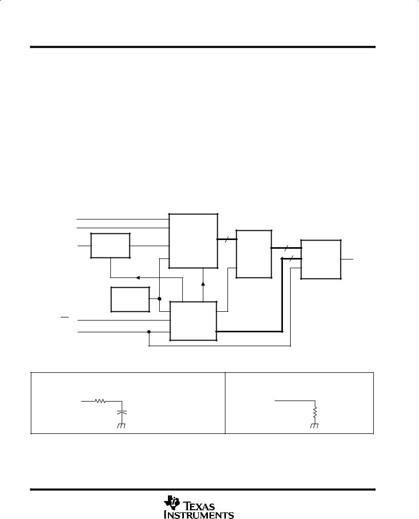
functional block diagram |
|
|
|
|
|
|
||
REF + |
1 |
|
|
|
|
|
|
|
3 |
|
8-Bit |
|
|
|
|
|
|
REF ± |
|
|
|
|
|
|
||
|
|
Analog-to |
|
|
|
|
|
|
|
|
|
8 |
|
|
|
|
|
|
|
Sample |
Digital |
|
|
|
|
|
|
2 |
|
8 |
|
|
|
||
ANALOG IN |
and |
Converter |
Output |
|
|
|
||
|
8-to-1 Data |
|
|
|||||
|
|
Hold |
(Switched- |
Data |
4 |
6 |
|
|
|
|
Selector |
DATA |
|||||
|
|
|
Capacitors) |
Regiser |
||||
|
|
|
|
and |
|
OUT |
||
|
|
|
|
|
|
|||
|
|
|
|
|
|
|
||
|
|
|
|
|
|
Driver |
|
|
|
|
|
Internal |
|
|
|
|
|
|
|
|
System |
|
|
|
|
|
|
|
|
Clock |
|
|
|
|
|
|
5 |
|
Control |
|
|
|
|
|
CS |
|
Logic and |
|
|
|
|
|
|
|
|
|
|
|
|
|
||
I/O CLOCK |
7 |
|
Output Counter |
|
|
|
|
|
|
|
|
|
|
|
|
|
|
typical equivalent inputs
INPUT CIRCUIT IMPEDANCE DURING SAMPLING MODE
1 kΩ TYP
ANALOG IN
Ci = 60 pF TYP (equivalent input capacitance)
INPUT CIRCUIT IMPEDANCE DURING HOLD MODE
ANALOG IN
5 MΩ TYP
2 |
POST OFFICE BOX 655303 •DALLAS, TEXAS 75265 |

TLC548C, TLC548I, TLC549C, TLC549I 8-BIT ANALOG-TO-DIGITAL CONVERTERS WITH SERIAL CONTROL
SLAS067C ± NOVEMBER 1983 ± REVISED SEPTEMBER 1996
operating sequence
|
1 |
2 |
3 |
4 |
5 |
|
6 |
7 |
8 |
|
1 |
2 |
3 |
4 |
5 |
|
6 |
7 |
8 |
I/O |
|
|
|
|
|
|
|
|
|
Don't |
Care |
|
|
|
|
|
|
|
|
CLOCK |
|
Access |
|
|
|
|
|
|
tconv |
|
Access |
|
|
Sample |
|
||||
|
|
|
|
Sample |
|
|
|
|
|
||||||||||
|
|
|
|
|
|
Cycle C |
|
|
|
||||||||||
tsu(CS) |
|
Cycle B |
|
|
|
|
|
|
|
Cycle C |
|
||||||||
|
|
|
|
|
Cycle B |
|
(see Note A) |
|
|
|
|
|
|||||||
|
|
|
|
|
|
|
|
|
|
|
|
|
|
||||||
|
|
|
|
|
|
|
|
|
|
|
tsu(CS) |
|
|
|
|
|
|
|
|
CS |
|
|
|
|
|
|
|
|
|
|
|
|
|
|
|
|
|
|
|
|
|
|
|
|
|
|
|
|
|
twH(CS) |
|
|
|
|
|
|
|
Hi-Z State |
|
|
|
|
|
|
|
|
|
|
|
Hi-Z State |
|
|
|
|
|
|
|
|
|
DATA |
A7 |
A6 |
A5 |
A4 |
A3 |
A2 |
A1 |
A0 |
|
B7 |
B6 |
B5 |
B4 |
B3 |
B2 |
B1 |
B0 |
|
|
|
|
|
|||||||||||||||||
OUT |
|
|
|
||||||||||||||||
|
|
|
|
|
|
|
|
|
|
|
|
|
|
|
|
|
|
|
|
|
|
|
|
|
|
|
|
|
A7 |
|
|
|
|
|
|
|
|
|
B7 |
|
|
Previous Conversion Data A |
|
|
|
Conversion Data B |
|
|
|||||||||||
|
|
|
|
|
|
|
|
||||||||||||
|
MSB |
|
|
|
|
|
LSB |
MSB |
|
MSB |
|
|
|
|
|
LSB |
MSB |
||
|
(see Note B) |
|
|
|
|
|
|
|
ten |
|
|
|
|
|
|
|
|
||
ten |
|
|
|
|
|
|
|
|
|
|
|
|
|
|
|
|
|
|
|
|
|
|
|
|
|
|
|
|
|
|
|
|
|
|
|
|
|
|
|
NOTES: A. The conversion cycle, which requires 36 internal system clock periods (17 μs maximum), is initiated with the eighth I/O clock pulse trailing edge after CS goes low for the channel whose address exists in memory at the time.
B.The most significant bit (A7) is automatically placed on the DATA OUT bus after CS is brought low. The remaining seven bits (A6±A0) are clocked out on the first seven I/O clock falling edges. B7±B0 follows in the same manner.
absolute maximum ratings over operating free-air temperature range (unless otherwise noted)
Supply voltage, VCC (see Note 1) . . . . . . . . . . . . . . . . . . . . . . . . . . . . . . . . . . . . . . . . . . . . |
. . . . . . . . . . . . . . 6.5 |
V |
Input voltage range at any input . . . . . . . . . . . . . . . . . . . . . . . . . . . . . . . . . . . . . . . . . . . . . |
±0.3 V to VCC + 0.3 |
V |
Output voltage range . . . . . . . . . . . . . . . . . . . . . . . . . . . . . . . . . . . . . . . . . . . . . . . . . . . . . . |
±0.3 V to VCC + 0.3 |
V |
Peak input current range (any input) . . . . . . . . . . . . . . . . . . . . . . . . . . . . . . . . . . . . . . . . . . |
. . . . . . . . . . . ± 10 mA |
|
Peak total input current range (all inputs) . . . . . . . . . . . . . . . . . . . . . . . . . . . . . . . . . . . . . . |
. . . . . . . . . . . ± 30 mA |
|
Operating free-air temperature range, TA (see Note 2): TLC548C, TLC549C . . . . . |
. . . . . . . . 0°C to 70°C |
|
TLC548I, TLC549I . . . . . . . |
. . . . . ±40°C to 85°C |
|
Storage temperature range, Tstg . . . . . . . . . . . . . . . . . . . . . . . . . . . . . . . . . . . . . . . . . . . . . . |
. . . . ±65°C to 150°C |
|
Lead temperature 1,6 mm (1/16 inch) from case for 10 seconds . . . . . . . . . . . . . . . . . . |
. . . . . . . . . . . . . 260°C |
|
NOTES: 1. All voltage values are with respect to the network ground terminal with the REF± and GND terminals connected together, unless otherwise noted.
2. The D package is not recommended below ± 40°C.
POST OFFICE BOX 655303 •DALLAS, TEXAS 75265 |
3 |
 Loading...