


Texas Instruments TLC372MP, TLC372MJG, TLC372MJGB, TLC372MFKB, TLC372MDR Datasheet
...TLC372, TLC372Q, TLC372Y
LinCMOS DUAL DIFFERENTIAL COMPARATORS
SLCS114B ± NOVEMBER 1983 ± REVISED MARCH 1999
DSingle or Dual-Supply Operation
DWide Range of Supply Voltages 2 V to 18 V
DVery Low Supply Current Drain 150 µA Typ at 5 V
DFast Response Time . . . 200 ns Typ for TTL-Level Input Step
DBuilt-in ESD Protection
DHigh Input Impedance . . . 1012 Ω Typ
DExtremely Low Input Bias Current
5 pA Typ
TLC372C, TLC372I, TLC372M, TLC372Q
D, P, OR PW PACKAGE
TLC372M . . . JG PACKAGE
|
|
(TOP VIEW) |
|
||
1OUT |
|
|
|
|
VCC |
|
1 |
8 |
|
||
|
|
||||
1IN ± |
|
|
|
|
|
|
2 |
7 |
|
2OUT |
|
1IN + |
|
3 |
6 |
|
2IN ± |
|
|
||||
GND |
|
4 |
5 |
|
2IN + |
|
|
||||
|
|
|
|
|
|
|
|
|
|
|
|
TLC372M . . . FK PACKAGE
(TOP VIEW)
DUltrastable Low Input Offset Voltage
DInput Offset Voltage Change at Worst-Case Input Conditions Typically 0.23 µV/Month,
Including the First 30 Days
DCommon-Mode Input Voltage Range Includes Ground
DOutput Compatible With TTL, MOS, and CMOS
DPin-Compatible With LM393
description
|
NC |
1OUT |
NC |
DD |
NC |
|
|
V |
|
||||
NC |
3 |
2 |
1 |
20 19 |
NC |
|
4 |
|
|
|
18 |
||
1IN ± |
5 |
|
|
|
17 |
2OUT |
NC |
6 |
|
|
|
16 |
NC |
1IN + |
7 |
|
|
|
15 |
2IN ± |
NC |
8 |
|
|
|
14 |
NC |
|
9 |
10 11 12 13 |
|
|||
|
NC |
GND |
NC |
2IN+ |
NC |
|
This device is fabricated using LinCMOS technology and consists of two independent voltage comparators, each designed to operate from a single power supply. Operation from dual supplies is also possible if the difference between the two supplies is 2 V to 18 V. Each device features extremely high input impedance (typically greater than 1012 Ω), allowing direct interfacing with high-impedance sources. The outputs are n-channel open-drain configurations and can be connected to achieve positive-logic wired-AND relationships.
NC ± No internal connection
symbol (each comparator)
IN +
OUT
IN ±
The TLC372 has internal electrostatic discharge (ESD) protection circuits and has been classified with a 1000-V ESD rating using human body model testing. However, care should be exercised in handling this device as exposure to ESD may result in a degradation of the device parametric performance.
The TLC372C is characterized for operation from 0°C to 70°C. The TLC372I is characterized for operation from ±40°C to 85°C. The TLC372M is characterized for operation over the full military temperature range of ±55°C to 125°C. The TLC372Q is characterized for operation from ±40°C to 125°C.
Please be aware that an important notice concerning availability, standard warranty, and use in critical applications of Texas Instruments semiconductor products and disclaimers thereto appears at the end of this data sheet.
LinCMOS is a trademark of Texas Instruments Incorporated.
PRODUCTION DATA information is current as of publication date. Products conform to specifications per the terms of Texas Instruments standard warranty. Production processing does not necessarily include testing of all parameters.
Copyright 1999, Texas Instruments Incorporated
POST OFFICE BOX 655303 •DALLAS, TEXAS 75265 |
1 |
TLC372, TLC372Q, TLC372Y
LinCMOS DUAL DIFFERENTIAL COMPARATORS
SLCS114B ± NOVEMBER 1983 ± REVISED MARCH 1999
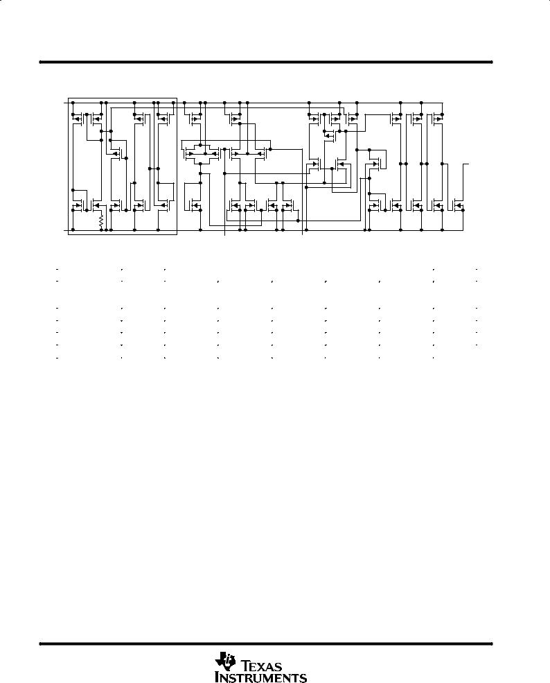
equivalent schematic (each comparator)
Common to All Channels
VDD |
|
|
OUT |
GND |
|
IN + |
IN ± |
AVAILABLE OPTIONS
|
|
|
PACKAGED DEVICES |
|
CHIP |
||
|
VIO max |
|
|
|
|
|
|
TA |
SMALL |
CHIP |
CERAMIC |
PLASTIC |
TSSOP |
FORM |
|
AT 25°C |
OUTLINE |
CARRIER |
DIP |
DIP |
|||
|
|
(PW) |
(Y) |
||||
|
|
(D) |
(FK) |
(JG) |
(P) |
|
|
|
|
|
|
||||
0°C to 70°C |
5 mV |
TLC372CD |
Ð |
Ð |
TLC372CP |
TLC372CPW |
TLC372Y |
|
|
|
|
|
|
|
|
± 40°C to 85°C |
5 mV |
TLC372ID |
Ð |
Ð |
TLC372IP |
Ð |
Ð |
|
|
|
|
|
|
|
|
± 55°C to 125°C |
5 mV |
TLC372MD |
TLC372MFK |
TLC372MJG |
TLC372MP |
Ð |
Ð |
|
|
|
|
|
|
|
|
± 40°C to 125°C |
5 mV |
TLC372QD |
Ð |
Ð |
TLC372QP |
Ð |
Ð |
|
|
|
|
|
|
|
|
The D packages are available taped and reeled. Add R suffix to device type (e.g., TLC372CDR).
2 |
POST OFFICE BOX 655303 •DALLAS, TEXAS 75265 |

TLC372, TLC372Q, TLC372Y
LinCMOS DUAL DIFFERENTIAL COMPARATORS
SLCS114B ± NOVEMBER 1983 ± REVISED MARCH 1999
TLC372Y chip information
These chips, when properly assembled, display characteristics similar to the TLC372C. Thermal compression or ultrasonic bonding can be used on the doped-aluminum bonding pads. Chips can be mounted with conductive epoxy or a gold-silicon preform.
|
|
|
|
|
|
BONDING PAD ASSIGNMENTS |
|
||
|
|
|
|
|
|
|
|
|
|
|
|
|
|
|
(7) |
(6) |
(5) |
||
|
|
|
(8) |
|
|
|
|
||
57 |
|
|
|
|
(4) |
||||
|
|
|
|
|
|
|
|
|
|
|
|
|
|
|
(1) |
(2) |
(3) |
||
|
|
|
|
|
|
|
|
|
|
|
|
|
|
|
|
|
|
|
|
|
|
|
|
|
|
|
57 |
|
|
|
|
|
|
|
|
|
|
|
|
|
|
|
VCC + |
|
|
||
|
(3) |
|
|
|
(8) |
|
|
1IN + |
+ |
|
|
|
|
||
|
|
|
(1) |
1OUT |
|||
|
|
|
|||||
|
|
|
|
|
|
||
1IN ± |
(2) |
± |
|
|
|
||
|
|
|
|||||
|
|
|
|
||||
|
|
|
(5) |
|
|||
|
|
||||||
|
|
+ |
2IN + |
||||
2OUT |
(7) |
|
|||||
|
|||||||
|
|
|
|
|
|||
|
|
|
|
± |
(6) |
2IN ± |
|
|
|
|
|
|
|||
|
|
|
|
|
|||
|
|
|
|||||
|
|
|
|
(4) |
|
|
|
|
|
|
GND |
|
|
||
CHIP THICKNESS: 15 TYPICAL BONDING PADS: 3.6 × 3.6 MINIMUM TJmax = 150°C
TOLERANCES ARE ± 10%.
ALL DIMENSIONS ARE IN MILS.
PIN (4) INTERNALLY CONNECTED TO BACKSIDE OF CHIP.
POST OFFICE BOX 655303 •DALLAS, TEXAS 75265 |
3 |
TLC372, TLC372Q, TLC372Y
LinCMOS DUAL DIFFERENTIAL COMPARATORS
SLCS114B ± NOVEMBER 1983 ± REVISED MARCH 1999
absolute maximum ratings over operating free-air temperature range (unless otherwise noted)²
Supply voltage, VDD (see Note 1) . . . . . . . . . . . . . . . . . . . . . . . . . . . . . . . . . . . . . . . |
. . . . . . . . . . . |
. . . . . . . . . . 18 |
V |
Differential input voltage, VID (see Note 2 . . . . . . . . . . . . . . . . . . . . . . . . . . . . . . . . |
. . . . . . . . . . . . |
. . . . . . . . ± 18 |
V |
Input voltage range, VI . . . . . . . . . . . . . . . . . . . . . . . . . . . . . . . . . . . . . . . . . . . . . . . . . |
. . . . . . . . . . . . |
±0.3 V to 18 |
V |
Output voltage, VO . . . . . . . . . . . . . . . . . . . . . . . . . . . . . . . . . . . . . . . . . . . . . . . . . . . . |
. . . . . . . . . . . . |
. . . . . . . . . 18 |
V |
Input current, II . . . . . . . . . . . . . . . . . . . . . . . . . . . . . . . . . . . . . . . . . . . . . . . . . . . . . . . |
. . . . . . . . . . . . |
. . . . . . . ± 5 mA |
|
Output current, IO . . . . . . . . . . . . . . . . . . . . . . . . . . . . . . . . . . . . . . . . . . . . . . . . . . . . . |
. . . . . . . . . . . . |
. . . . . . . 20 mA |
|
Duration of output short circuit to ground (see Note 3) . . . . . . . . . . . . . . . . . . . . . |
. . . . . . . . . . . . |
. . . . . unlimited |
|
Continuous total power dissipation . . . . . . . . . . . . . . . . . . . . . . . . . . . . . . . . . . . . . |
See Dissipation Rating Table |
||
Operating free-air temperature range, TA: TLC372C . . . . . . . . . . . . . . . . . . . . . . . |
. . . . . . . . . . . . |
. . 0°C to 70°C |
|
TLC372I . . . . . . . . . . . . . . . . . . . . . . . . |
. . . . . . . . . . . . |
±40°C to 85°C |
|
TLC372M . . . . . . . . . . . . . . . . . . . . . . . |
. . . . . . . . . . . |
±55°C to 125°C |
|
TLC372Q . . . . . . . . . . . . . . . . . . . . . . . |
. . . . . . . . . . . |
±40°C to 125°C |
|
Storage temperature range . . . . . . . . . . . . . . . . . . . . . . . . . . . . . . . . . . . . . . . . . . . . . |
. . . . . . . . . . . |
±65°C to 150°C |
|
Case temperature for 60 seconds: FK package . . . . . . . . . . . . . . . . . . . . . . . . . . . |
. . . . . . . . . . . . |
. . . . . . . 260°C |
|
Lead temperature 1,6 mm (1/16 inch) from case for 10 seconds: D, P, or PW package . . . . . |
. . . . . . . 260°C |
||
Lead temperature 1,6 mm (1/16 inch) from case for 60 seconds: JG package . |
. . . . . . . . . . . . |
. . . . . . . 300°C |
|
²Stresses beyond those listed under ªabsolute maximum ratingsº may cause permanent damage to the device. These are stress ratings only, and functional operation of the device at these or any other conditions beyond those indicated under ªrecommended operating conditionsº is not
implied. Exposure to absolute-maximum-rated conditions for extended periods may affect device reliability. NOTES: 1. All voltage values except differential voltages are with respect to network ground.
2.Differential voltages are at IN+ with respect to IN ±.
3.Short circuits from outputs to VDD can cause excessive heating and eventual device destruction.
DISSIPATION RATING TABLE
PACKAGE |
TA ≤ 25°C |
DERATING |
DERATE |
TA = 70°C |
TA = 85°C |
TA = 125°C |
|
POWER RATING |
FACTOR |
ABOVE TA |
POWER RATING |
POWER RATING |
POWER RATING |
||
|
|||||||
D |
500 mW |
5.8 mW/°C |
64°C |
464 mW |
377 mW |
145 mW |
|
FK |
500 mW |
11.0 mW/°C |
104°C |
500 mW |
500 mW |
275 mW |
|
JG |
500 mW |
8.4 mW/°C |
90°C |
500 mW |
500 mW |
210 mW |
|
P |
500 mW |
8.0 mW/°C |
87°C |
500 mW |
500 mW |
200 mW |
|
PW |
525 mW |
4.2 mW/°C |
25°C |
336 mW |
N/A |
N/A |
|
|
|
|
|
|
|
|
recommended operating conditions
|
|
TLC372C |
TLC372I |
TLC372M |
TLC372Q |
UNIT |
|||||
|
|
|
|
|
|
|
|
|
|
||
|
|
MIN |
MAX |
MIN |
MAX |
MIN |
MAX |
MIN |
MAX |
||
|
|
|
|||||||||
|
|
|
|
|
|
|
|
|
|
|
|
Supply voltage, VDD |
|
3 |
16 |
3 |
16 |
4 |
16 |
4 |
16 |
V |
|
Common-mode input voltage, VIC |
VDD = 5 V |
0 |
3.5 |
0 |
3.5 |
0 |
3.5 |
0 |
3.5 |
V |
|
VDD = 10 V |
0 |
8.5 |
0 |
8.5 |
0 |
8.5 |
0 |
8.5 |
|||
|
|
||||||||||
Operating free-air temperature, TA |
|
0 |
70 |
± 40 |
85 |
± 55 |
125 |
± 40 |
125 |
°C |
|
4 |
POST OFFICE BOX 655303 •DALLAS, TEXAS 75265 |
 Loading...