


Texas Instruments TLC4502AMJGB, TLC4502AMJG, TLC4502AMFKB, TLC4502AMD, TLC4502AID Datasheet
...
TLC4501, TLC4501A, TLC4502, TLC4502A
FAMILY OF SELF-CALIBRATING (Self-Cal )
PRECISION CMOS RAIL-TO-RAIL OUTPUT OPERATIONAL AMPLIFIERS
SLOS221A ± MAY 1998 ± REVISED JULY 1999
DSelf-Calibrates Input Offset Voltage to 40 V Max
DLow Input Offset Voltage Drift . . . 1 V/°C
DInput Bias Current . . . 1 pA
DOpen Loop Gain . . . 120 dB
DRail-To-Rail Output Voltage Swing
DStable Driving 1000 pF Capacitive Loads
DGain Bandwidth Product . . . 4.7 MHz
description
DSlew Rate . . . 2.5 V/ s
DHigh Output Drive Capability . . . ±50 mA
DCalibration Time . . . 300 ms
DCharacterized From ±55°C to 125°C
DAvailable in Q-Temp Automotive HighRel Automotive Applications Configuration Control / Print Support Qualification to Automotive Standards
The TLC4501 and TLC4502 are the highest precision CMOS single supply rail-to-rail operational amplifiers available today. The input offset voltage is 10 V typical and 40 V maximum. This exceptional precision, combined with a 4.7-MHz bandwidth, 2.5-V/ s slew rate, and 50-mA output drive, is ideal for multiple applications including: data acquisition systems, measurement equipment, industrial control applications, and portable digital scales.
These amplifiers feature self-calibrating circuitry which digitally trims the input offset voltage to less than 40 V within the first 300 ms of operation. The offset is then digitally stored in an integrated successive approximation register (SAR). Immediately after the data is stored, the calibration circuitry effectively drops out of the signal path, shuts down, and the device functions as a standard operational amplifier.
3 |
|
Offset Control |
|
IN+ |
+ |
|
|
|
|
1 |
|
|
|
OUT |
|
2 |
± |
|
|
IN± |
|
||
Calibration Circuitry |
|
||
|
|
SAR |
|
|
D/A |
A/D |
|
8 |
5 V |
4 |
|
VDD |
|
||
|
|
GND |
|
Power-On |
Control |
Oscillator |
|
Reset |
Logic |
||
|
|||
Figure 1. Channel One of the TLC4502
Please be aware that an important notice concerning availability, standard warranty, and use in critical applications of Texas Instruments semiconductor products and disclaimers thereto appears at the end of this data sheet.
LinEPIC and Self-Cal are trademarks of Texas Instruments Incorporated.
PRODUCTION DATA information is current as of publication date. Products conform to specifications per the terms of Texas Instruments standard warranty. Production processing does not necessarily include testing of all parameters.
Copyright 1999, Texas Instruments Incorporated
On products compliant to MIL-PRF-38535, all parameters are tested unless otherwise noted. On all other products, production processing does not necessarily include testing of all parameters.
POST OFFICE BOX 655303 •DALLAS, TEXAS 75265 |
1 |
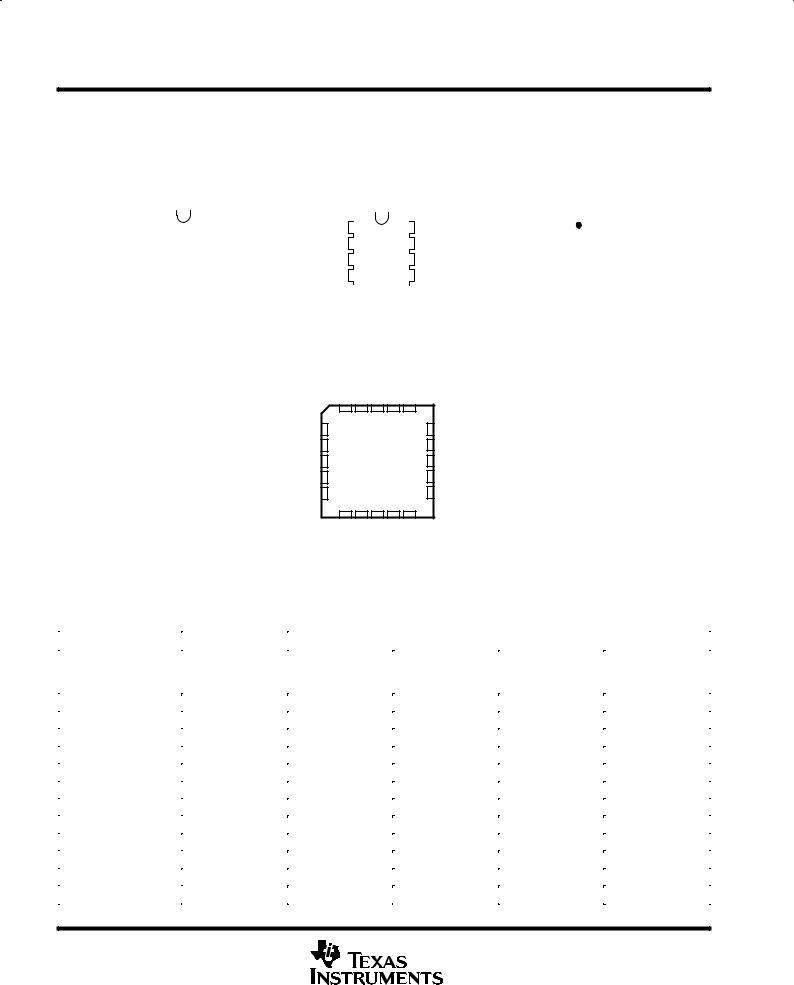
TLC4501, TLC4501A, TLC4502, TLC4502A
FAMILY OF SELF-CALIBRATING (Self-Cal )
PRECISION CMOS RAIL-TO-RAIL OUTPUT OPERATIONAL AMPLIFIERS
SLOS221A ± MAY 1998 ± REVISED JULY 1999
description (continued)
Using this technology eliminates the need for noisy and expensive chopper techniques, laser trimming, and power hungry, split supply bipolar operational amplifiers.
|
|
TLC4501 |
|
|
TLC4502 |
|
|
|
TLC4502 |
|
|||||||
|
|
D PACKAGE |
|
D OR JG PACKAGE |
|
U PACKAGE |
|
||||||||||
|
|
(TOP VIEW) |
|
|
(TOP VIEW) |
|
|
(TOP VIEW) |
|
||||||||
NC |
|
|
|
|
|
NC |
|
|
|
|
|
NC |
|
|
|
|
NC |
|
1 |
8 |
|
|
1OUT |
1 |
8 |
|
VDD+ |
|
1 |
10 |
|
||||
1IN ± |
|
2 |
7 |
|
|
VDD+ |
1IN ± |
2 |
7 |
|
2OUT |
1OUT |
|
2 |
9 |
|
VDD + |
1IN + |
|
3 |
6 |
|
|
OUT |
1IN + |
3 |
6 |
|
2IN ± |
1IN ± |
|
3 |
8 |
|
2OUT |
VDD ±/GND |
|
4 |
5 |
|
|
NC |
VDD ±/GND |
4 |
5 |
|
2IN+ |
1IN + |
|
4 |
7 |
|
2IN ± |
|
|
|
|
|
|
|
|
|
|
|
|
VDD ±/GND |
|
5 |
6 |
|
2IN + |
|
|
|
|
|
|
|
|
|
|
|
|
|
|
||||
|
|
|
|
|
|
|
|
|
|
|
|
|
|
||||
|
|
TLC4502 |
|
|
||
|
FK PACKAGE |
|
||||
|
(TOP VIEW) |
|
||||
|
NC |
1OUT |
NC |
DD+ |
NC |
|
|
V |
|
||||
NC |
3 |
2 |
1 |
20 19 |
NC |
|
4 |
|
|
|
18 |
||
1IN ± |
5 |
|
|
|
17 |
2OUT |
NC |
6 |
|
|
|
16 |
NC |
1IN + |
7 |
|
|
|
15 |
2IN ± |
NC |
8 |
|
|
|
14 |
NC |
|
9 |
10 11 12 13 |
|
|||
|
NC |
/GND |
NC |
2IN+ |
NC |
|
|
|
DD± |
|
|
|
|
|
|
V |
|
|
|
|
AVAILABLE OPTIONS
|
|
|
|
PACKAGED DEVICES |
|
||
|
|
|
|
|
|
|
|
TA |
VIOmax AT 25°C |
SMALL |
CHIP CARRIER |
CERAMIC DIP |
CERAMIC FLAT |
||
OUTLINE² |
PACK |
||||||
|
|
|
(FK) |
(JG) |
|||
|
|
|
(D) |
(U) |
|||
|
|
|
|
|
|||
|
|
|
|
|
|
|
|
|
40 |
V |
TLC4501ACD |
Ð |
Ð |
Ð |
|
|
|
|
|
|
|
|
|
0°C to 70°C |
50 |
V |
TLC4502ACD |
Ð |
Ð |
Ð |
|
|
|
|
|
|
|
||
80 |
V |
TLC4501CD |
Ð |
Ð |
Ð |
||
|
|||||||
|
|
|
|
|
|
|
|
|
100 |
V |
TLC4502CD |
Ð |
Ð |
Ð |
|
|
|
|
|
|
|
|
|
|
40 |
V |
TLC4501AID |
Ð |
Ð |
Ð |
|
|
|
|
|
|
|
|
|
±40°C to 125°C |
50 |
V |
TLC4502AID |
Ð |
Ð |
Ð |
|
|
|
|
|
|
|
||
80 |
V |
TLC4501ID |
Ð |
Ð |
Ð |
||
|
|||||||
|
|
|
|
|
|
|
|
|
100 |
V |
TLC4502ID |
Ð |
Ð |
Ð |
|
|
|
|
|
|
|
|
|
±40°C to 125°C |
50 |
V |
TLC4502AQD |
Ð |
Ð |
Ð |
|
|
|
|
|
|
|
||
100 |
V |
TLC4502QD |
Ð |
Ð |
Ð |
||
|
|||||||
|
|
|
|
|
|
|
|
±55°C to 125°C |
50 |
V |
TLC4502AMD |
TLC4502AMFKB |
TLC4502AMJGB |
TLC4502AMUB |
|
|
|
|
|
|
|
||
100 |
V |
TLC4502MD |
TLC4502MFKB |
TLC4502MJGB |
TLC4502MUB |
||
|
|||||||
|
|
|
|
|
|
|
|
² The D package is also available taped and reeled.
2 |
POST OFFICE BOX 655303 •DALLAS, TEXAS 75265 |
TLC4501, TLC4501A, TLC4502, TLC4502A
FAMILY OF SELF-CALIBRATING (Self-Cal )
PRECISION CMOS RAIL-TO-RAIL OUTPUT OPERATIONAL AMPLIFIERS
SLOS221A ± MAY 1998 ± REVISED JULY 1999
absolute maximum ratings over operating free-air temperature range (unless otherwise noted)²
Supply voltage, VDD + (see Note 1) . . . . . . . . . . . . . . . . . . . . . . . . . . . . . . . . . . . . . . |
. . . . . . . . . . . . . . . . . . . . . . 7 V |
Differential input voltage, VID (see Note 2) . . . . . . . . . . . . . . . . . . . . . . . . . . . . . . . |
. . . . . . . . . . . . . . . . . . . . . ± 7 V |
Input voltage range, VI (any input, see Note 1) . . . . . . . . . . . . . . . . . . . . . . . . . . . . |
. . . . . . . . . . . . . ±0.3 V to 7 V |
Input current, II (each input) . . . . . . . . . . . . . . . . . . . . . . . . . . . . . . . . . . . . . . . . . . . . |
. . . . . . . . . . . . . . . . . . . ± 5 mA |
Output current, IO (each output) . . . . . . . . . . . . . . . . . . . . . . . . . . . . . . . . . . . . . . . . |
. . . . . . . . . . . . . . . . . ± 100 mA |
Total current into VDD + . . . . . . . . . . . . . . . . . . . . . . . . . . . . . . . . . . . . . . . . . . . . . . . . |
. . . . . . . . . . . . . . . . . ± 100 mA |
Total current out of VDD ±/GND . . . . . . . . . . . . . . . . . . . . . . . . . . . . . . . . . . . . . . . . . |
. . . . . . . . . . . . . . . . . ± 100 mA |
Electrostatic discharge (ESD) . . . . . . . . . . . . . . . . . . . . . . . . . . . . . . . . . . . . . . . . . . |
. . . . . . . . . . . . . . . . . . . > 2 kV |
Duration of short-circuit current at (or below) 25°C (see Note 3) . . . . . . . . . . . . . |
. . . . . . . . . . . . . . . . . unlimited |
Continuous total power dissipation . . . . . . . . . . . . . . . . . . . . . . . . . . . . . . . . . . . . . |
See Dissipation Rating Table |
Operating free-air temperature range, TA: TLC4502C . . . . . . . . . . . . . . . . . . . . . . |
. . . . . . . . . . . . . . 0°C to 70°C |
TLC4502I . . . . . . . . . . . . . . . . . . . . . . . |
. . . . . . . . . . . ±40°C to 125°C |
TLC4502Q . . . . . . . . . . . . . . . . . . . . . . |
. . . . . . . . . . . ±40°C to 125°C |
TLC4502M . . . . . . . . . . . . . . . . . . . . . . |
. . . . . . . . . . . ±55°C to 125°C |
Storage temperature range, Tstg . . . . . . . . . . . . . . . . . . . . . . . . . . . . . . . . . . . . . . . . |
. . . . . . . . . . . ±65°C to 150°C |
Case temperature for 60 seconds, TC: FK package . . . . . . . . . . . . . . . . . . . . . . . |
. . . . . . . . . . . . . . . . . . . 260°C |
Lead temperature 1,6 mm (1/16 inch) from case for 10 seconds . . . . . . . . . . . . |
. . . . . . . . . . . . . . . . . . . 260°C |
²Stresses beyond those listed under ªabsolute maximum ratingsº may cause permanent damage to the device. These are stress ratings only, and functional operation of the device at these or any other conditions beyond those indicated under ªrecommended operating conditionsº is not
implied. Exposure to absolute-maximum-rated conditions for extended periods may affect device reliability. NOTES: 1. All voltage values, except differential voltages, are with respect to VDD ±/GND .
2. Differential voltages are at IN+ with respect to IN ±. Excessive current flows when an input is brought below VDD ± ± 0.3 V.
3.The output may be shorted to either supply. Temperature and/or supply voltages must be limited to ensure that the maximum dissipation rating is not exceeded.
DISSIPATION RATING TABLE
PACKAGE |
TA ≤ 25°C |
DERATING FACTOR |
TA = 70°C |
TA = 85°C |
TA = 125°C |
|
POWER RATING |
ABOVE TA = 25°C |
POWER RATING |
POWER RATING |
POWER RATING |
||
|
||||||
D |
725 mW |
5.8 mW/°C |
464 mW |
377 mW |
145 mW |
|
FK |
1375 mW |
11.0 mW/°C |
880 mW |
715 mW |
275 mW |
|
JG |
1050 mW |
8.4 mW/°C |
672 mW |
546 mW |
210 mW |
|
U |
675 mW |
5.4 mW/°C |
432 mW |
350 mW |
135 mW |
recommended operating conditions
|
TLC4502C |
TLC4502I |
TLC4502Q |
TLC4502M |
UNIT |
||||
|
|
|
|
|
|
|
|
|
|
|
MIN |
MAX |
MIN |
MAX |
MIN |
MAX |
MIN |
MAX |
|
|
|
||||||||
|
|
|
|
|
|
|
|
|
|
Supply voltage, VDD |
4 |
6 |
4 |
6 |
4 |
6 |
4 |
6 |
V |
Input voltage range, VI |
VDD ± |
VDD+ ± 2.3 |
VDD ± |
VDD+ ± 2.3 |
VDD ± |
VDD+ ± 2.3 |
VDD ± |
VDD+ ± 2.3 |
V |
Common-mode input voltage, VIC |
VDD ± |
VDD+ ± 2.3 |
VDD ± |
VDD+ ± 2.3 |
VDD ± |
VDD+ ± 2.3 |
VDD ± |
VDD+ ± 2.3 |
V |
Operating free-air temperature, TA |
0 |
70 |
± 40 |
125 |
± 40 |
125 |
± 55 |
125 |
°C |
POST OFFICE BOX 655303 •DALLAS, TEXAS 75265 |
3 |
TLC4501, TLC4501A, TLC4502, TLC4502A
FAMILY OF SELF-CALIBRATING (Self-Cal )
PRECISION CMOS RAIL-TO-RAIL OUTPUT OPERATIONAL AMPLIFIERS
SLOS221A ± MAY 1998 ± REVISED JULY 1999
electrical characteristics at specified free-air temperature, VDD = 5 V, GND = 0 (unless otherwise noted)
|
PARAMETER |
TEST CONDITIONS |
T ² |
TLC450xC |
|
UNIT |
||||
|
|
|
|
|||||||
|
|
|
|
|||||||
|
|
|
|
|
A |
MIN |
TYP |
MAX |
|
|
|
|
|
|
|
|
|
||||
|
|
|
|
TLC4501 |
|
±80 |
10 |
80 |
|
|
|
|
|
|
|
|
|
|
|
|
|
VIO |
Input offset voltage |
VDD = ± 2.5 V, |
VO = 0, |
TLC4501A |
Full range |
±40 |
10 |
40 |
µV |
|
VIC = 0, |
RS = 50 Ω |
TLC4502 |
±100 |
10 |
100 |
|||||
|
|
|
|
|||||||
|
|
|
|
TLC4502A |
|
±50 |
10 |
50 |
|
|
|
|
|
|
|
|
|
|
|
|
|
VIO |
Temperature coefficient of input |
|
|
|
Full range |
|
1 |
|
µV/°C |
|
offset voltage |
|
|
|
|
|
|||||
|
|
|
|
|
|
|
|
|
||
|
|
|
|
|
|
|
|
|
|
|
IIO |
Input offset current |
VDD = ± 2.5 V, |
VO = 0, |
|
25°C |
|
1 |
|
pA |
|
|
|
|
|
|
||||||
|
|
VIC = 0, |
RS = 50 Ω |
|
Full range |
|
|
500 |
|
|
IIB |
Input bias current |
|
|
|
25°C |
|
1 |
|
pA |
|
|
|
|
Full range |
|
|
500 |
||||
|
|
|
|
|
|
|
|
|||
|
|
|
|
|
|
|
|
|
|
|
|
|
IOH = ± 500 µA |
|
|
25°C |
|
4.99 |
|
|
|
VOH |
High-level output voltage |
IOH = ± 5 mA |
|
|
25°C |
|
4.9 |
|
V |
|
|
|
|
|
Full range |
4.7 |
|
|
|
||
|
|
|
|
|
|
|
|
|||
|
|
|
|
|
|
|
|
|
||
|
|
VIC = 2.5 V, |
IOL = 500 µA |
25°C |
|
0.01 |
|
|
||
VOL |
Low-level output voltage |
VIC = 2.5 V, |
IOL = 5 mA |
|
25°C |
|
0.1 |
|
V |
|
|
|
|
Full range |
|
|
0.3 |
|
|||
|
|
|
|
|
|
|
|
|||
|
|
|
|
|
|
|
|
|
||
AVD |
Large-signal differential voltage |
VIC = 2.5 V, |
VO = 1 V to 4 V, |
25°C |
200 |
1000 |
|
V/mV |
||
amplification |
RL = 1 kΩ, |
See Note 4 |
|
Full range |
200 |
|
|
|||
|
|
|
|
|
||||||
RI(D) |
Differential input resistance |
|
|
|
25°C |
|
10 |
|
kΩ |
|
RL |
Input resistance |
See Note 4 |
|
|
25°C |
|
1012 |
|
Ω |
|
CL |
Common-mode input capacitance |
f = 10 kHz, |
P package |
|
25°C |
|
8 |
|
pF |
|
zO |
Closed-loop output impedance |
AV = 10, |
f = 100 kHz |
|
25°C |
|
1 |
|
Ω |
|
CMRR |
Common-mode rejection ratio |
VIC = 0 to 2.7 V, |
VO = 2.5 V, |
25°C |
90 |
100 |
|
dB |
||
RS = 1 kΩ |
|
|
Full range |
85 |
|
|
||||
|
|
|
|
|
|
|
||||
kSVR |
Supply-voltage rejection ratio |
VDD = 4 V to 6 V, VIC = 0, |
No load |
25°C |
90 |
100 |
|
dB |
||
( VDD ± / VIO) |
Full range |
90 |
|
|
||||||
|
|
|
|
|
|
|
||||
|
|
|
|
TLC4501/A |
25°C |
|
1 |
1.5 |
|
|
IDD |
Supply current |
VO = 2.5 V, |
No load |
Full range |
|
|
2 |
mA |
||
|
|
|
||||||||
|
|
|
|
|
||||||
TLC4502/A |
25°C |
|
2.5 |
3.5 |
||||||
|
|
|
|
|
|
|||||
|
|
|
|
|
|
|
|
|
||
|
|
|
|
Full range |
|
|
4 |
|
||
|
|
|
|
|
|
|
|
|||
|
|
|
|
|
|
|
|
|
|
|
VIT(CAL) |
Calibration input threshold voltage |
|
|
|
Full range |
4 |
|
|
V |
|
² Full range is 0°C to 70°C. |
|
|
|
|
|
|
|
|
||
NOTE 4: RL and CL values are referenced to 2.5 V. |
|
|
|
|
|
|
|
|||
4 |
POST OFFICE BOX 655303 •DALLAS, TEXAS 75265 |

TLC4501, TLC4501A, TLC4502, TLC4502A
FAMILY OF SELF-CALIBRATING (Self-Cal )
PRECISION CMOS RAIL-TO-RAIL OUTPUT OPERATIONAL AMPLIFIERS
SLOS221A ± MAY 1998 ± REVISED JULY 1999
operating characteristics, VDD = 5 V
|
PARAMETER |
TEST CONDITIONS |
T ² |
TLC450xC, TLC450xAC |
UNIT |
|||||||
|
|
|
|
|||||||||
|
|
|
|
|||||||||
|
|
|
|
A |
MIN |
TYP |
MAX |
|
|
|
|
|
|
|
|
|
|
|
|
|
|
|
|||
SR |
Slew rate at unity gain |
VO = 0.5 V to 2.5 V, |
CL = 100 pF |
25°C |
1.5 |
2.5 |
|
V/µs |
||||
|
|
|
|
|
|
|
|
|
||||
Full range |
1 |
|
|
V/µs |
||||||||
|
|
|
|
|
|
|||||||
Vn |
Equivalent input noise voltage |
f = 10 Hz |
|
25°C |
|
70 |
|
|
|
|
|
|
|
|
|
|
|
|
nV/√ |
Hz |
|
||||
f = 1 kHz |
|
25°C |
|
12 |
|
|
||||||
|
|
|
|
|
|
|
|
|
|
|||
VN(PP) |
Peak-to-peak equivalent input noise |
f = 0.1 to 1 Hz |
|
25°C |
|
1 |
|
µV |
||||
voltage |
f = 0.1 to 10 Hz |
|
25°C |
|
1.5 |
|
||||||
|
|
|
|
|
|
|
|
|
||||
|
|
|
|
25°C |
|
|
|
|
||||
In |
Equivalent input noise current |
|
|
|
0.6 |
|
fA/√ |
Hz |
|
|||
|
|
VO = 0.5 V to 2.5 V, |
AV = 1 |
25°C |
|
0.02% |
|
|
|
|
|
|
|
|
f = 10 kHz, |
|
|
|
|
|
|
|
|
|
|
THD + N Total harmonic distortion plus noise |
AV = 10 |
25°C |
|
0.08% |
|
|
|
|
|
|
||
RL = 1 kΩ, |
|
|
|
|
|
|
|
|||||
|
|
|
25°C |
|
|
|
|
|
|
|
|
|
|
|
CL = 100 pF |
AV = 100 |
|
0.55% |
|
|
|
|
|
|
|
|
Gain-bandwidth product |
f = 10 kHz, |
RL = 1 kΩ, |
25°C |
|
4.7 |
|
MHz |
||||
|
CL = 100 pF |
|
|
|
||||||||
|
|
|
|
|
|
|
|
|
|
|
|
|
BOM |
Maximum output swing bandwidth |
VO(PP) = 2 V, |
AV = 1, |
25°C |
|
1 |
|
MHz |
||||
RL = 1 kΩ, |
CL = 100 pF |
|
|
|||||||||
|
|
|
|
|
|
|
|
|
|
|
||
|
|
AV = ±1, |
to 0.1% |
25°C |
|
1.6 |
|
|
|
|
|
|
ts |
Settling time |
Step = 0.5 V to 2.5 V, |
|
|
|
|
|
µs |
||||
RL = 1 kΩ, |
to 0.01% |
25°C |
|
2.2 |
|
|||||||
|
|
CL = 100 pF |
|
|
|
|
|
|
|
|||
|
|
|
|
|
|
|
|
|
|
|
|
|
φm |
Phase margin at unity gain |
RL = 1 kΩ, |
CL = 100 pF |
25°C |
|
74 |
|
|
|
|
|
|
|
Calibration time |
|
|
25°C |
|
300 |
|
ms |
||||
|
|
|
|
|
|
|
|
|
|
|
|
|
² Full range is 0°C to 70°C. |
|
|
|
|
|
|
|
|
|
|
|
|
NOTE 4: RL and CL values are referenced to 2.5 V. |
|
|
|
|
|
|
|
|
|
|
||
POST OFFICE BOX 655303 •DALLAS, TEXAS 75265 |
5 |
TLC4501, TLC4501A, TLC4502, TLC4502A
FAMILY OF SELF-CALIBRATING (Self-Cal )
PRECISION CMOS RAIL-TO-RAIL OUTPUT OPERATIONAL AMPLIFIERS
SLOS221A ± MAY 1998 ± REVISED JULY 1999
electrical characteristics at specified free-air temperature, VDD = 5 V, GND = 0 (unless otherwise noted)
|
PARAMETER |
TEST CONDITIONS |
T ² |
|
TLC450xI |
|
UNIT |
|||
|
|
|
|
|||||||
|
|
|
|
|||||||
|
|
|
|
|
A |
MIN |
TYP |
MAX |
|
|
|
|
|
|
|
|
|
||||
|
|
|
|
TLC4501 |
|
±80 |
10 |
80 |
|
|
|
|
|
|
|
|
|
|
|
|
|
VIO |
Input offset voltage |
VDD = ± 2.5 V, |
VO = 0, |
TLC4501A |
Full range |
±40 |
10 |
40 |
µV |
|
VIC = 0, |
RS = 50 Ω |
TLC4502 |
±100 |
10 |
100 |
|||||
|
|
|
|
|||||||
|
|
|
|
TLC4502A |
|
±50 |
10 |
50 |
|
|
|
|
|
|
|
|
|
|
|
|
|
VIO |
Temperature coefficient of input |
|
|
|
Full range |
|
1 |
|
µV/°C |
|
offset voltage |
|
|
|
|
|
|||||
|
|
|
|
|
|
|
|
|
||
|
|
|
|
|
|
|
|
|
|
|
|
|
VDD = ± 2.5 V, |
VO = 0, |
|
25°C |
|
1 |
|
|
|
IIO |
Input offset current |
VIC = 0, |
RS = 50 Ω |
|
± 40°C to |
|
|
500 |
pA |
|
|
|
|
85°C |
|
|
|
||||
|
|
|
|
|
Full range |
|
|
5 |
nA |
|
|
|
|
|
|
|
|
|
|
|
|
|
|
|
|
|
25°C |
|
1 |
|
|
|
|
|
VDD = ± 2.5 V, |
|
|
|
|
|
|
pA |
|
IIB |
Input bias current |
VO = 0, |
|
± 40°C to |
|
|
500 |
|||
VIC = 0, |
RS = 50 Ω |
|
85°C |
|
|
|
||||
|
|
|
|
|
Full range |
|
|
10 |
nA |
|
|
|
|
|
|
|
|
|
|
|
|
|
|
IOH = ± 500 µA |
|
|
25°C |
|
4.99 |
|
|
|
VOH |
High-level output voltage |
IOH = ± 5 mA |
|
|
25°C |
|
4.9 |
|
V |
|
|
|
|
|
Full range |
4.7 |
|
|
|
||
|
|
|
|
|
|
|
|
|||
|
|
|
|
|
|
|
|
|
||
|
|
VIC = 2.5 V, |
IOL = 500 µA |
25°C |
|
0.01 |
|
|
||
VOL |
Low-level output voltage |
VIC = 2.5 V, |
IOL = 5 mA |
|
25°C |
|
0.1 |
|
V |
|
|
|
|
Full range |
|
|
0.3 |
|
|||
|
|
|
|
|
|
|
|
|||
|
|
|
|
|
|
|
|
|
||
AVD |
Large-signal differential voltage |
VIC = 2.5 V, |
VO = 1 V to 4 V, |
25°C |
200 |
1000 |
|
V/mV |
||
amplification |
RL = 1 kΩ, |
See Note 4 |
|
Full range |
200 |
|
|
|||
|
|
|
|
|
||||||
RI(D) |
Differential input resistance |
|
|
|
25°C |
|
10 |
|
kΩ |
|
RL |
Input resistance |
See Note 4 |
|
|
25°C |
|
1012 |
|
Ω |
|
CL |
Common-mode input capacitance |
f = 10 kHz, |
P package |
|
25°C |
|
8 |
|
pF |
|
zO |
Closed-loop output impedance |
AV = 10, |
f = 100 kHz |
|
25°C |
|
1 |
|
Ω |
|
CMRR |
Common-mode rejection ratio |
VIC = 0 to 2.7 V, |
VO = 2.5 V, |
25°C |
90 |
100 |
|
dB |
||
RS = 1 kΩ |
|
|
Full range |
85 |
|
|
||||
|
|
|
|
|
|
|
||||
kSVR |
Supply-voltage rejection ratio |
VDD = 4 V to 6 V, VIC = 0, |
No load |
25°C |
90 |
100 |
|
dB |
||
( VDD ± / VIO) |
Full range |
90 |
|
|
||||||
|
|
|
|
|
|
|
||||
|
|
|
|
TLC4501/A |
25°C |
|
1 |
1.5 |
|
|
|
|
|
|
|
|
|
|
|
||
IDD |
Supply current |
VO = 2.5 V, |
No load |
Full range |
|
|
2 |
mA |
||
|
|
|
||||||||
|
|
|
|
|
||||||
TLC4502/A |
25°C |
|
2.5 |
3.5 |
||||||
|
|
|
|
|
|
|||||
|
|
|
|
Full range |
|
|
4 |
|
||
|
|
|
|
|
|
|
|
|||
|
|
|
|
|
|
|
|
|
|
|
VIT(CAL) |
Calibration input threshold voltage |
|
|
|
Full range |
4 |
|
|
V |
|
² Full range is ± 40°C to 125°C. |
|
|
|
|
|
|
|
|
||
NOTE 4: RL and CL values are referenced to 2.5 V. |
|
|
|
|
|
|
|
|||
6 |
POST OFFICE BOX 655303 •DALLAS, TEXAS 75265 |
TLC4501, TLC4501A, TLC4502, TLC4502A
FAMILY OF SELF-CALIBRATING (Self-Cal )
PRECISION CMOS RAIL-TO-RAIL OUTPUT OPERATIONAL AMPLIFIERS
SLOS221A ± MAY 1998 ± REVISED JULY 1999
operating characteristics, VDD = 5 V
|
PARAMETER |
TEST CONDITIONS |
T ² |
TLC450xI, TLC450xAI |
UNIT |
|||||||
|
|
|
|
|||||||||
|
|
|
|
|||||||||
|
|
|
|
A |
MIN |
TYP |
MAX |
|
|
|
|
|
|
|
|
|
|
|
|
|
|
|
|||
SR |
Slew rate at unity gain |
VO = 0.5 V to 2.5 V, |
CL = 100 pF |
25°C |
1.5 |
2.5 |
|
V/µs |
||||
|
|
|
|
|
|
|
|
|
||||
Full range |
1 |
|
|
V/µs |
||||||||
|
|
|
|
|
|
|||||||
Vn |
Equivalent input noise voltage |
f = 10 Hz |
|
25°C |
|
70 |
|
|
|
|
|
|
|
|
|
|
|
|
nV/√ |
Hz |
|
||||
f = 1 kHz |
|
25°C |
|
12 |
|
|
||||||
|
|
|
|
|
|
|
|
|
|
|||
VN(PP) |
Peak-to-peak equivalent input noise |
f = 0.1 to 1 Hz |
|
25°C |
|
1 |
|
µV |
||||
voltage |
f = 0.1 to 10 Hz |
|
25°C |
|
1.5 |
|
||||||
|
|
|
|
|
|
|
|
|
||||
In |
Equivalent input noise current |
|
|
25°C |
|
0.6 |
|
fA/√ |
|
|
|
|
|
|
|
|
Hz |
|
|||||||
|
|
VO = 0.5 V to 2.5 V, |
AV = 1 |
25°C |
|
0.02% |
|
|
|
|
|
|
|
|
f = 10 kHz, |
|
|
|
|
|
|
|
|
|
|
THD + N Total harmonic distortion plus noise |
AV = 10 |
25°C |
|
0.08% |
|
|
|
|
|
|
||
RL = 1 kΩ, |
|
|
|
|
|
|
|
|||||
|
|
|
25°C |
|
|
|
|
|
|
|
|
|
|
|
CL = 100 pF |
AV = 100 |
|
0.55% |
|
|
|
|
|
|
|
|
Gain-bandwidth product |
f = 10 kHz, |
RL = 1 kΩ, |
25°C |
|
4.7 |
|
MHz |
||||
|
CL = 100 pF |
|
|
|
||||||||
|
|
|
|
|
|
|
|
|
|
|
|
|
BOM |
Maximum output swing bandwidth |
VO(PP) = 2 V, |
AV = 1, |
25°C |
|
1 |
|
MHz |
||||
RL = 1 kΩ, |
CL = 100 pF |
|
|
|||||||||
|
|
|
|
|
|
|
|
|
|
|
||
|
|
AV = ±1, |
to 0.1% |
25°C |
|
1.6 |
|
|
|
|
|
|
ts |
Settling time |
Step = 0.5 V to 2.5 V, |
|
|
|
|
|
µs |
||||
RL = 1 kΩ, |
to 0.01% |
25°C |
|
2.2 |
|
|||||||
|
|
CL = 100 pF |
|
|
|
|
|
|
|
|||
|
|
|
|
|
|
|
|
|
|
|
|
|
φm |
Phase margin at unity gain |
RL = 1 kΩ, |
CL = 100 pF |
25°C |
|
74 |
|
|
|
|
|
|
|
Calibration time |
|
|
25°C |
|
300 |
|
ms |
||||
|
|
|
|
|
|
|
|
|
|
|
|
|
² Full range is ± 40°C to 125°C. |
|
|
|
|
|
|
|
|
|
|
|
|
NOTE 4: RL and CL values are referenced to 2.5 V. |
|
|
|
|
|
|
|
|
|
|
||
POST OFFICE BOX 655303 •DALLAS, TEXAS 75265 |
7 |

TLC4501, TLC4501A, TLC4502, TLC4502A
FAMILY OF SELF-CALIBRATING (Self-Cal )
PRECISION CMOS RAIL-TO-RAIL OUTPUT OPERATIONAL AMPLIFIERS
SLOS221A ± MAY 1998 ± REVISED JULY 1999
electrical characteristics at specified free-air temperature, VDD = 5 V, GND = 0 (unless otherwise noted)
|
|
|
|
|
|
|
TLC4502Q, |
|
|
|
|
PARAMETER |
TEST CONDITIONS |
T ² |
TLC4502M |
|
UNIT |
||||
|
|
|
|
|
|
A |
|
|
|
|
|
|
|
|
|
|
|
MIN |
TYP |
MAX |
|
|
|
|
|
|
|
|
|
|
|
|
VIO |
Input offset voltage |
VDD = ± 2.5 V, |
VO = 0, |
|
TLC4502 |
Full range |
±100 |
10 |
100 |
µV |
VIC = 0, |
RS = 50 Ω |
|
TLC4502A |
±50 |
10 |
50 |
||||
|
|
|
|
|
||||||
VIO |
Temperature coefficient of input |
|
|
|
|
Full range |
|
1 |
|
µV/°C |
offset voltage |
|
|
|
|
|
|
||||
|
|
|
|
|
|
|
|
|
|
|
|
|
|
|
|
|
|
|
|
|
|
IIO |
Input offset current |
VDD = ± 2.5 V, |
VO = 0, |
|
25°C |
|
1 |
|
nA |
|
|
125°C |
|
|
|
||||||
|
|
VIC = 0, |
RS = 50 Ω |
|
|
|
5 |
|
||
IIB |
Input bias current |
|
|
|
|
25°C |
|
1 |
|
nA |
|
|
|
|
|
|
|
|
|||
|
|
|
|
125°C |
|
|
10 |
|||
|
|
|
|
|
|
|
|
|
||
|
|
|
|
|
|
|
|
|
|
|
|
|
IOH = ± 500 µA |
|
|
|
25°C |
|
4.99 |
|
|
VOH |
High-level output voltage |
IOH = ± 5 mA |
|
|
|
25°C |
|
4.9 |
|
V |
|
|
|
|
|
Full range |
4.7 |
|
|
|
|
|
|
|
|
|
|
|
|
|
||
|
|
|
|
|
|
|
|
|
|
|
|
|
VIC = 2.5 V, |
IOL = 500 µA |
|
25°C |
|
0.01 |
|
|
|
VOL |
Low-level output voltage |
VIC = 2.5 V, |
IOL = 5 mA |
|
25°C |
|
0.1 |
|
V |
|
|
|
|
Full range |
|
|
0.3 |
|
|||
|
|
|
|
|
|
|
|
|
||
|
|
|
|
|
|
|
|
|
||
AVD |
Large-signal differential voltage |
VIC = 2.5 V, |
VO = 1 V to 4 V, |
25°C |
200 |
1000 |
|
V/mV |
||
amplification |
RL = 1 kΩ, |
See Note 4 |
|
Full range |
200 |
|
|
|||
|
|
|
|
|
||||||
RI(D) |
Differential input resistance |
|
|
|
|
25°C |
|
10 |
|
kΩ |
RL |
Input resistance |
See Note 4 |
|
|
|
25°C |
|
1012 |
|
Ω |
CL |
Common-mode input capacitance |
f = 10 kHz, |
P package |
|
25°C |
|
8 |
|
pF |
|
zO |
Closed-loop output impedance |
AV = 10, |
f = 100 kHz |
|
25°C |
|
1 |
|
Ω |
|
CMRR |
Common-mode rejection ratio |
VIC = 0 to 2.7 V, |
VO = 2.5 V, |
|
25°C |
90 |
100 |
|
dB |
|
RS = 1 kΩ |
|
|
|
Full range |
85 |
|
|
|||
|
|
|
|
|
|
|
|
|||
kSVR |
Supply-voltage rejection ratio |
VDD = 4 V to 6 V, VIC = VDD /2, |
25°C |
90 |
100 |
|
dB |
|||
( VDD ± / VIO) |
No load |
|
|
|
Full range |
90 |
|
|
||
|
|
|
|
|
|
|
||||
IDD |
Supply current |
VO = 2.5 V, |
No load |
|
25°C |
|
2.5 |
3.5 |
mA |
|
|
|
|
|
|
||||||
|
Full range |
|
|
4 |
||||||
|
|
|
|
|
|
|
|
|
||
|
|
|
|
|
|
|
|
|
|
|
VIT(CAL) |
Calibration input threshold voltage |
|
|
|
|
Full range |
4 |
|
|
V |
² Full range is ± 40°C to 125°C for Q suffix, ± 55°C to 125°C for M suffix. NOTE 4: RL and CL values are referenced to 2.5 V.
8 |
POST OFFICE BOX 655303 •DALLAS, TEXAS 75265 |

TLC4501, TLC4501A, TLC4502, TLC4502A
FAMILY OF SELF-CALIBRATING (Self-Cal )
PRECISION CMOS RAIL-TO-RAIL OUTPUT OPERATIONAL AMPLIFIERS
|
|
|
|
SLOS221A ± MAY 1998 ± REVISED JULY 1999 |
|||||||||
|
|
|
|
|
|
|
|
|
|
|
|
|
|
operating characteristics, VDD = 5 V |
|
|
|
|
|
|
|
|
|
|
|
||
|
|
|
|
|
TLC4502Q, TLC4502M, |
|
|
|
|
|
|
||
|
PARAMETER |
TEST CONDITIONS |
T ² |
TLC4502AQ, |
|
UNIT |
|
||||||
|
TLC4502AM |
|
|
||||||||||
|
|
|
|
A |
|
|
|
|
|
|
|
||
|
|
|
|
|
MIN |
TYP |
MAX |
|
|
|
|
|
|
|
|
|
|
|
|
|
|
|
|
|
|
|
|
SR |
Slew rate at unity gain |
VO = 0.5 V to 2.5 V, |
CL = 100 pF |
25°C |
1.5 |
2.5 |
|
V/µs |
|
||||
See Note 4 |
|
Full range |
1 |
|
|
V/µs |
|
||||||
|
|
|
|
|
|
||||||||
|
|
|
|
|
|
|
|
|
|
|
|
|
|
Vn |
Equivalent input noise voltage |
f = 10 Hz |
|
25°C |
|
70 |
|
|
|
|
|
|
|
|
|
|
|
|
|
nV/√ |
Hz |
|
|
||||
f = 1 kHz |
|
25°C |
|
12 |
|
|
|
||||||
|
|
|
|
|
|
|
|
|
|
|
|||
|
|
|
|
|
|
|
|
|
|
|
|
|
|
VN(PP) |
Peak-to-peak equivalent input noise |
f = 0.1 to 1 Hz |
|
25°C |
|
1 |
|
µV |
|
||||
voltage |
f = 0.1 to 10 Hz |
|
25°C |
|
1.5 |
|
|
||||||
|
|
|
|
|
|
|
|
|
|
||||
|
|
|
|
|
|
|
|
|
|
|
|
||
|
|
|
|
25°C |
|
|
|
|
|
||||
In |
Equivalent input noise current |
|
|
|
0.6 |
|
fA/√ |
Hz |
|
|
|||
|
|
VO = 0.5 V to 2.5 V, |
AV = 1 |
25°C |
|
0.02% |
|
|
|
|
|
|
|
|
|
f = 10 kHz, |
|
|
|
|
|
|
|
|
|
|
|
THD + N |
Total harmonic distortion plus noise |
AV = 10 |
25°C |
|
0.08% |
|
|
|
|
|
|
|
|
RL = 1 kΩ, |
|
|
|
|
|
|
|
|
|||||
|
|
|
25°C |
|
|
|
|
|
|
|
|
|
|
|
|
CL = 100 pF |
AV = 100 |
|
0.55% |
|
|
|
|
|
|
|
|
|
Gain-bandwidth product |
f = 10 kHz, |
RL = 1 kΩ, |
25°C |
|
4.7 |
|
MHz |
|
||||
|
CL = 100 pF |
|
|
|
|
||||||||
|
|
|
|
|
|
|
|
|
|
|
|
|
|
BOM |
Maximum output swing bandwidth |
VO(PP) = 2 V, |
AV = 1, |
25°C |
|
1 |
|
MHz |
|
||||
RL = 1 kΩ, |
CL = 100 pF |
|
|
|
|||||||||
|
|
|
|
|
|
|
|
|
|
|
|
||
|
|
AV = ±1, |
to 0.1% |
25°C |
|
1.6 |
|
|
|
|
|
|
|
ts |
Settling time |
Step = 0.5 V to 2.5 V, |
|
|
|
|
|
µs |
|
||||
RL = 1 kΩ, |
to 0.01% |
25°C |
|
2.2 |
|
|
|||||||
|
|
CL = 100 pF |
|
|
|
|
|
|
|
|
|||
|
|
|
|
|
|
|
|
|
|
|
|
|
|
φm |
Phase margin at unity gain |
RL = 1 kΩ, |
CL = 100 pF |
25°C |
|
74 |
|
|
|
|
|
|
|
|
Calibration time |
|
|
25°C |
|
300 |
|
ms |
|
||||
|
|
|
|
|
|
|
|
|
|
|
|
|
|
² Full range is ± 40°C to 125°C for Q suffix, ± 55°C to 125°C for M suffix. |
|
|
|
|
|
|
|
|
|
|
|
||
NOTE 4: RL and CL values are referenced to 2.5 V. |
|
|
|
|
|
|
|
|
|
|
|
||
POST OFFICE BOX 655303 •DALLAS, TEXAS 75265 |
9 |

TLC4501, TLC4501A, TLC4502, TLC4502A
FAMILY OF SELF-CALIBRATING (Self-Cal )
PRECISION CMOS RAIL-TO-RAIL OUTPUT OPERATIONAL AMPLIFIERS
SLOS221A ± MAY 1998 ± REVISED JULY 1999
TYPICAL CHARACTERISTICS
Table of Graphs
|
|
|
FIGURE |
|
|
|
|
|
|
VIO |
Input offset voltage |
Distribution |
2, 3, 4 |
|
|
|
|||
vs Common-mode input voltage |
5 |
|||
|
|
|||
|
|
|
|
|
αVIO |
Input offset voltage temperature coefficient |
Distribution |
6, 7 |
|
VOH |
High-level output voltage |
vs High-level output current |
8 |
|
VOL |
Low-level output voltage |
vs Low-level output current |
9 |
|
VO(PP) |
Maximum peak-to-peak output voltage |
vs Frequency |
10 |
|
IOS |
Short-circuit output current |
vs Free-air temperature |
11 |
|
VO |
Output voltage |
vs Differential input voltage |
12 |
|
AVD |
Large-signal differential voltage amplification |
vs Free-air temperature |
13 |
|
vs Frequency |
14 |
|||
|
|
|||
|
|
|
|
|
zo |
Output impedance |
vs Frequency |
15 |
|
CMRR |
Common-mode rejection ratio |
vs Frequency |
16 |
|
vs Free-air temperature |
17 |
|||
|
|
|||
|
|
|
|
|
SR |
Slew rate |
vs Load capacitance |
18 |
|
vs Free-air temperature |
19 |
|||
|
|
|||
|
|
|
|
|
|
Inverting large-signal pulse response |
|
20 |
|
|
|
|
|
|
|
Voltage-follower large-signal pulse response |
|
21 |
|
|
|
|
|
|
|
Inverting small-signal pulse response |
|
22 |
|
|
|
|
|
|
|
Voltage-follower small-signal pulse response |
|
23 |
|
|
|
|
|
|
Vn |
Equivalent input noise voltage |
vs Frequency |
24 |
|
|
Input noise voltage |
Over a 10-second period |
25 |
|
|
|
|
|
|
THD + N |
Total harmonic distortion plus noise |
vs Frequency |
26 |
|
|
|
|
|
|
|
Gain-bandwidth product |
vs Free-air temperature |
27 |
|
|
|
|
|
|
φm |
Phase margin |
vs Load capacitance |
28 |
|
|
|
|||
vs Frequency |
14 |
|||
|
|
|||
|
|
|
|
|
|
Gain margin |
vs Load capacitance |
29 |
|
|
|
|
|
|
PSRR |
Power-supply rejection ratio |
vs Free-air temperature |
30 |
|
|
|
|
|
|
|
Calibration time at ± 40°C |
|
31 |
|
|
Calibration time at 25°C |
|
32 |
|
|
|
|
|
|
|
Calibration time at 85°C |
|
33 |
|
|
|
|
|
|
|
Calibration time at 125°C |
|
34 |
|
|
|
|
|
10 |
POST OFFICE BOX 655303 •DALLAS, TEXAS 75265 |
 Loading...