


Texas Instruments TLC0834IDR, TLC0834ID, TLC0834CN, TLC0834CD, TLC0834CDR Datasheet
...TLC0834C, TLC0834I, TLC0838C, TLC0838I 8-BIT ANALOG-TO-DIGITAL CONVERTERS WITH SERIAL CONTROL
SLAS094C ± MARCH 1995 ± REVISED APRIL 1997
D 8-Bit Resolution |
TLC0834 . . . D OR N PACKAGE |
||||||||||
D Easy Microprocessor Interface or |
|
|
|
(TOP VIEW) |
|
|
|
||||
|
|
|
|
|
|
|
|
|
|
||
Stand-Alone Operation |
NC |
|
|
|
|
VCC |
|||||
1 |
14 |
|
|
||||||||
D Operates Ratiometrically or With 5-V |
|
|
|||||||||
|
CS |
|
2 |
13 |
|
|
DI |
||||
Reference |
|
|
|
||||||||
CH0 |
3 |
12 |
|
|
CLK |
||||||
D 4- or 8-Channel Multiplexer Options With |
|
|
|||||||||
CH1 |
4 |
11 |
|
|
SARS |
||||||
Address Logic |
|
|
|||||||||
CH2 |
5 |
10 |
|
|
DO |
||||||
D Input Range 0 to 5 V With Single 5-V Supply |
|
|
|||||||||
CH3 |
6 |
9 |
|
|
REF |
||||||
D Remote Operation With Serial Data Link |
DGTL GND |
7 |
8 |
|
|
ANLG GND |
|||||
D Inputs and Outputs Are Compatible With |
|
|
|
|
|
|
|
|
|
|
|
TLC0838 . . . DW OR N PACKAGE |
|||||||||||
TTL and MOS |
|||||||||||
D Conversion Time of 32 μs at |
|
|
|
(TOP VIEW) |
|
|
|
||||
|
|
|
|
|
|
|
|
|
|
||
fclock = 250 kHz |
CH0 |
|
1 |
20 |
|
|
VCC |
||||
|
|
|
|||||||||
D Functionally Equivalent to the ADC0834 |
|
|
|
||||||||
CH1 |
|
2 |
19 |
|
|
NC |
|||||
and ADC0838 Without the Internal Zener |
CH2 |
|
3 |
18 |
|
|
CS |
|
|||
Regulator Network |
CH3 |
|
4 |
17 |
|
|
DI |
||||
|
|
|
|||||||||
D Total Unadjusted Error . . . ±1 LSB |
CH4 |
|
5 |
16 |
|
|
CLK |
||||
|
|
|
|||||||||
description |
CH5 |
|
6 |
15 |
|
|
SARS |
||||
|
|
|
|||||||||
CH6 |
|
7 |
14 |
|
|
DO |
|||||
|
|
|
|||||||||
These devices are 8-bit successive- |
CH7 |
|
8 |
13 |
|
|
SE |
|
|||
|
|
|
|
|
|||||||
COM |
9 |
12 |
|
|
REF |
||||||
approximation analog-to-digital converters, each |
|
|
|||||||||
DGTL GND |
10 |
11 |
|
|
ANLG GND |
||||||
with an input-configurable multichannel |
|
|
|||||||||
|
|
|
|
|
|
|
|
|
|
||
multiplexer and serial input/output. The serial |
|
|
|
|
|
|
|
|
|
|
|
input/output is configured to interface with |
|
|
|
|
|
|
|
|
|
|
|
standard shift registers or microprocessors. |
|
|
|
|
|
|
|
|
|
|
|
Detailed information on interfacing with most |
|
|
|
|
|
|
|
|
|
|
|
popular microprocessors is readily available from |
|
|
|
|
|
|
|
|
|
|
|
the factory. |
|
|
|
|
|
|
|
|
|
|
|
The TLC0834 (4-channel) and TLC0838 (8-channel) multiplexer is software configured for single-ended or differential inputs as well as pseudo-differential input assignments. The differential analog voltage input allows for common-mode rejection or offset of the analog zero input voltage value. In addition, the voltage reference input can be adjusted to allow encoding of any smaller analog voltage span to the full 8 bits of resolution.
The TLC0834C and TLC0838C are characterized for operation from 0°C to 70°C. The TLC0834I and TLC0838I are characterized for operation from ±40°C to 85°C. The TLC0834Q is characterized for operation from ±40°C to 125°C.
|
|
AVAILABLE OPTIONS |
|
|
|
|
|
PACKAGE |
|
|
|
|
|
|
|
|
|
TA |
SMALL |
SMALL |
|
PLASTIC DIP |
|
OUTLINE |
OUTLINE |
|
|||
|
|
|
(N) |
||
|
(D) |
(DW) |
|
|
|
|
|
|
|
||
|
|
|
|
|
|
0°C to 70°C |
TLC0834CD |
TLC0838CDW |
|
TLC0834CN |
TLC0838CN |
|
|
|
|
|
|
± 40°C to 85°C |
TLC0834ID |
TLC0838IDW |
|
TLC0834IN |
TLC0838IN |
|
|
|
|
|
|
± 40°C to 125°C |
Ð |
Ð |
|
TLC0834QN |
Ð |
Please be aware that an important notice concerning availability, standard warranty, and use in critical applications of Texas Instruments semiconductor products and disclaimers thereto appears at the end of this data sheet.
PRODUCTION DATA information is current as of publication date. Products conform to specifications per the terms of Texas Instruments standard warranty. Production processing does not necessarily include testing of all parameters.
Copyright 1997, Texas Instruments Incorporated
POST OFFICE BOX 655303 •DALLAS, TEXAS 75265 |
2±1 |

2±2
75265 TEXAS DALLAS,• 655303 BOX OFFICE POST
functional block diagram
CLK 16
18 CS 
DI17 (see Note A)
TLC0838
Only
SE
CH0 1 TLC0834 CH1 2
CH2 3
CH3 4
TLC0838  CH4 5 CH5 6
CH6 7
CH7 8
COM 9
|
|
Start |
CS |
|
|
Flip-Flop |
|
|
|
|
18 |
|
|
CLK |
15 |
|
|
|
|
D |
R |
S |
SARS |
|
5-Bit Shift Register |
||
CLK |
R |
|
|
SELECT1 ODD\ EVEN SGL\ DIF START |
|
|
|
SELECT0 |
|
|
To Internal |
|
|
|
|
|
|
|
|
|
Circuits |
|
|
|
|
|
|
|
CLK |
|
|
|
|
|
|
|
|
|
|
|
|
Analog |
|
|
|
Time |
|
S |
|
|
|
|
|
|
|
R |
|
|||
|
MUX |
|
|
|
|
|
|||
|
|
|
|
Delay |
|
|
|
||
|
|
|
|
|
|
18 |
|
||
|
|
|
|
|
|
|
|
|
|
|
EN |
|
|
|
|
|
|
CS |
|
|
|
|
|
|
|
|
|
|
|
|
|
Comparator |
CS |
|
|
CS |
|
|
|
|
|
|
18 |
|
|
18 |
|
CS |
|
|
EN |
|
R |
|
|
R |
|
18 |
CS |
|
|
|
|
|
R |
18 |
|||
|
12 |
|
|
|
|
CLK |
|
||
REF |
|
SAR |
|
|
|
14 |
|||
Ladder |
|
|
|
|
EOC |
CLK |
|||
|
Bits 0±7 |
Logic |
Bits 0±7 |
9-Bit |
|
DO |
|||
|
and |
and |
|
|
|
||||
|
Decoder |
|
|
|
Shift |
|
D |
|
|
|
|
Latch |
|
|
|
|
|||
|
|
|
|
Bit 1 |
Register |
|
|
|
|
|
|
|
|
|
|
|
|
||
|
|
|
|
|
|
|
|
|
|
|
|
|
|
MSB |
LSB |
|
|
|
|
|
|
One |
|
First |
First |
|
|
|
|
|
|
|
|
|
|
|
|
|
|
|
|
Shot |
|
|
|
|
|
|
|
NOTE A: For the TLC0834, DI is input directly to the D input of SELECT1; SELECT0 is forced to a high.
B: Terminal numbers shown are for the DW or N package.
1997 APRIL REVISED ± 1995 MARCH ± SLAS094C |
CONVERTERS DIGITAL-TO-ANALOG BIT-8 |
TLC0838I TLC0838C, TLC0834I, TLC0834C, |
|
CONTROL SERIAL WITH |
|

TLC0834C, TLC0834I, TLC0838C, TLC0838I 8-BIT ANALOG-TO-DIGITAL CONVERTERS WITH SERIAL CONTROL
SLAS094C ± MARCH 1995 ± REVISED APRIL 1997
functional description
The TLC0834 and TLC0838 use a sample-data-comparator structure that converts differential analog inputs by a successive-approximation routine. Operation of both devices is similar with the exception of SE, an analog common input, and multiplexer addressing. The input voltage to be converted is applied to a channel terminal and is compared to ground (single ended), to an adjacent input (differential), or to a common terminal (pseudo differential) that can be an arbitrary voltage. The input terminals are assigned a positive (+) or negative (±) polarity. When the signal input applied to the assigned positive terminal is less than the signal on the negative terminal, the converter output is all zeros.
Channel selection and input configuration are under software control using a serial-data link from the controlling processor. A serial-communication format allows more functions to be included in a converter package with no increase in size. In addition, it eliminates the transmission of low-level analog signals by locating the converter at the analog sensor and communicating serially with the controlling processor. This process returns noise-free digital data to the processor.
A particular input configuration is assigned during the multiplexer-addressing sequence. The multiplexer address shifts into the converter through the data input (DI) line. The multiplexer address selects the analog inputs to be enabled and determines whether the input is single ended or differential. When the input is differential, the polarity of the channel input is assigned. Differential inputs are assigned to adjacent channel pairs. For example, channel 0 and channel 1 may be selected as a differential pair. These channels cannot act differentially with any other channel. In addition to selecting the differential mode, the polarity may also be selected. Either channel of the channel pair may be designated as the negative or positive input.
The common input on the TLC0838 can be used for a pseudo-differential input. In this mode, the voltage on the common input is considered to be the negative differential input for all channel inputs. This voltage can be any reference potential common to all channel inputs. Each channel input can then be selected as the positive differential input. This feature is useful when all analog circuits are biased to a potential other than ground.
A conversion is initiated by setting CS low, which enables all logic circuits. CS must be held low for the complete conversion process. A clock input is then received from the processor. On each low-to-high transition of the clock input, the data on DI is clocked into the multiplexer-address shift register. The first logic high on the input is the start bit. A 3- to 4-bit assignment word follows the start bit. On each successive low-to-high transition of the clock input, the start bit and assignment word are shifted through the shift register. When the start bit is shifted into the start location of the multiplexer register, the input channel is selected and conversion starts. The SAR status output (SARS) goes high to indicate that a conversion is in progress, and DI to the multiplexer shift register is disabled for the duration of the conversion.
An interval of one clock period is automatically inserted to allow the selected multiplexed channel to settle. DO comes out of the high-impedance state and provides a leading low for one clock period of multiplexer settling time. The SAR comparator compares successive outputs from the resistive ladder with the incoming analog signal. The comparator output indicates whether the analog input is greater than or less than the resistive-ladder output. As the conversion proceeds, conversion data is simultaneously output from DO, with the most significant bit (MSB) first. After eight clock periods, the conversion is complete and SARS goes low.
The TLC0834 outputs the least-significant-bit (LSB) first data after the MSB-first data stream. When SE is held high on the TLC0838, the value of the LSB remains on the data line. When SE is forced low, the data is then clocked out as LSB-first data. (To output LSB first, SE must first go low, then the data stored in the 9-bit shift register outputs LSB first.) When CS goes high, all internal registers are cleared. At this time, the output circuits go to the high-impedance state. If another conversion is desired, CS must make a high-to-low transition followed by address information.
DI and DO can be tied together and controlled by a bidirectional processor I/O bit received on a single wire. This is possible because DI is only examined during the multiplexer-addressing interval and DO is still in the high-impedance state.
POST OFFICE BOX 655303 •DALLAS, TEXAS 75265 |
2±3 |
TLC0834C, TLC0834I, TLC0838C, TLC0838I
8-BIT ANALOG-TO-DIGITAL CONVERTERS WITH SERIAL CONTROL
SLAS094C ± MARCH 1995 ± REVISED APRIL 1997
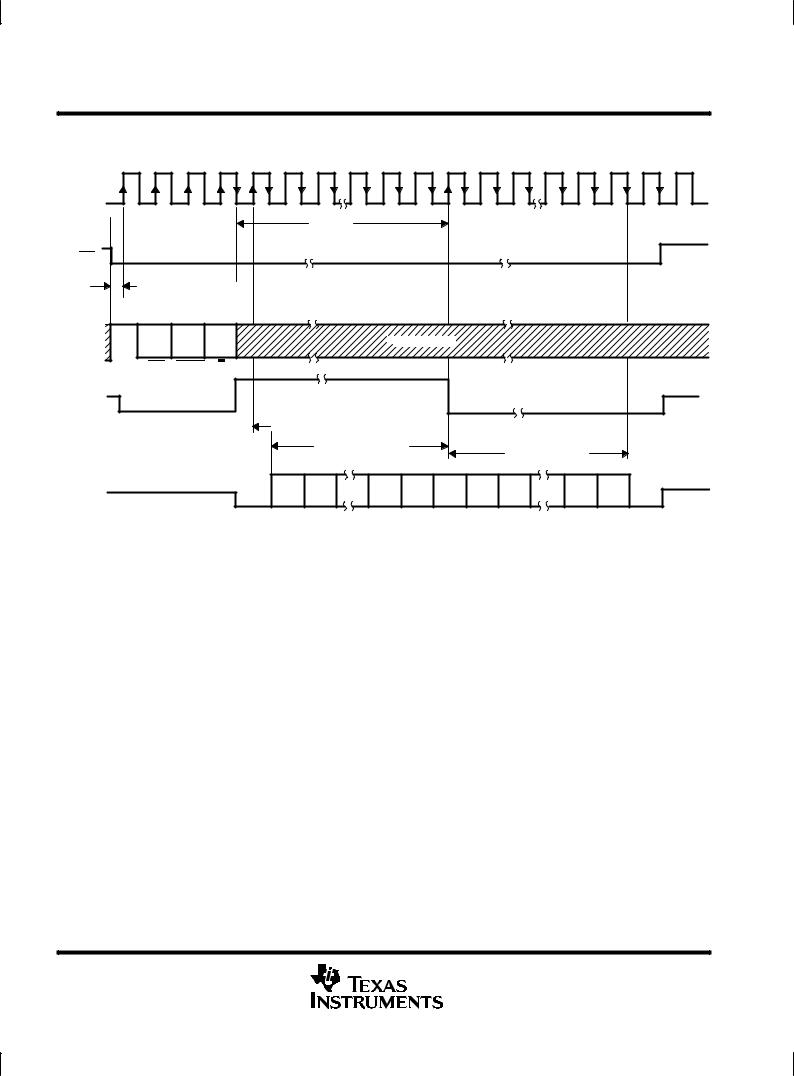
sequence of operation
|
|
|
|
|
|
|
TLC0834 |
|
|
|
|
|
|
|
|
|
1 |
2 |
3 |
4 |
5 |
6 |
7 |
10 |
11 |
12 |
13 |
14 |
15 |
18 |
19 |
20 |
21 |
CLK
|
|
|
tconv |
CS |
|
|
|
|
tsu |
+Sign |
|
|
|
SELECT |
|
Start |
SGL |
Bit |
|
Bit |
ODD |
Bit 1 |
|
DI |
|
|
Don't Care |
|
DIF |
EVEN |
1 |
Hi-Z |
|
|
|
SARS |
|
|
|
Mux Settling Time 
MSB-First Data
LSB-First Data
DO |
Hi-Z |
|
|
|
LSB |
|
|
|
Hi-Z |
MSB |
|
|
|
|
|
|
MSB |
||
|
7 |
6 |
2 |
1 |
0 |
1 |
2 |
6 |
7 |
TLC0834 MUX-ADDRESS CONTROL LOGIC TABLE
|
|
|
MUX ADDRESS |
|
CHANNEL NUMBER |
||||||
|
|
|
|
|
|
|
|
|
|
|
|
SGL/DIF |
|
ODD/EVEN |
|
SELECT BIT 1 |
CH0 |
CH1 CH2 |
CH3 |
||||
L |
L |
|
L |
+ |
± |
|
|
||||
L |
L |
|
H |
|
+ |
± |
|
||||
L |
H |
|
L |
± |
+ |
|
|
||||
L |
H |
|
H |
|
± |
+ |
|
||||
H |
L |
|
L |
+ |
+ |
|
|
||||
H |
L |
|
H |
|
|
|
|||||
H |
H |
|
L |
|
+ |
+ |
|
||||
H |
H |
|
H |
|
|
|
|||||
|
|
|
|
|
|||||||
H = high level, L = low level, ± or + = terminal polarity for the selected input channel
2±4 |
POST OFFICE BOX 655303 •DALLAS, TEXAS 75265 |

TLC0834C, TLC0834I, TLC0838C, TLC0838I 8-BIT ANALOG-TO-DIGITAL CONVERTERS WITH SERIAL CONTROL
SLAS094C ± MARCH 1995 ± REVISED APRIL 1997
sequence of operation
TLC0838
1 |
2 |
3 |
4 |
5 |
6 |
7 |
8 |
11 |
12 |
13 |
14 |
15 |
16 |
17 |
18 |
19 |
20 |
21 |
22 |
|
23 |
24 |
25 |
26 |
27 |
CLK |
|
|
|
|
|
|
|
|
|
|
|
|
|
|
|
|
|
|
|
|
|
|
|
|
|
|
tsu |
|
|
|
|
|
tconv |
|
|
|
|
|
|
|
|
|
|
|
|
|
|
|
|
|
|
CS |
|
|
|
|
|
|
|
|
|
|
|
|
|
|
|
|
|
|
|
|
|
|
|
|
|
|
|
Mux |
|
|
|
|
|
|
|
|
|
|
|
|
|
|
|
|
|
|
|
|
|
|
|
|
Addressing |
|
|
|
|
|
|
|
|
|
|
|
|
|
|
|
|
|
|
|
|
|
|
||
|
tsu |
+ |
|
|
|
|
|
|
|
|
|
|
|
|
|
|
|
|
|
|
|
|
|
|
|
Start |
|
Sign |
SEL |
SEL |
|
|
|
|
|
|
|
|
|
|
|
|
|
|
|
|
|
|
|
|
|
SGL |
Bit |
Bit |
Bit |
|
|
|
|
|
|
|
|
|
|
|
|
|
|
|
|
|
|
|
|
|
|
Bit |
ODD |
1 |
0 |
|
|
|
|
|
|
|
|
|
|
|
|
|
|
|
|
|
|
|
|
|
|
DI |
|
|
|
|
|
|
|
|
|
|
|
|
|
Don't Care |
|
|
|
|
|
|
|
|
|
|
|
|
|
|
|
|
|
|
|
|
|
|
|
|
|
|
|
|
|
|
|
|
|
|
|
|
|
|
DIF |
EVEN |
1 |
0 |
|
|
|
|
|
|
|
|
|
|
|
|
|
|
|
|
|
|
|
|
|
Hi-Z |
|
|
|
|
|
|
|
|
|
|
|
|
|
|
|
|
|
|
|
|
|
|
|
|
Hi-Z |
SARS |
|
|
|
|
|
|
|
|
|
|
|
|
|
|
|
|
|
|
|
|
|
|
|
|
|
SE |
|
|
|
|
|
|
|
|
|
|
|
|
|
|
|
|
|
|
|
|
|
|
|
|
|
|
|
|
|
|
|
|
MSB-First Data |
|
|
|
|
LSB-First Data |
|
|
|
|
|
|
|
|
|
|
|||
|
|
|
|
|
|
|
|
|
|
|
|
|
|
|
|
|
|
|
|
|
|
|
|||
Hi-Z |
|
|
|
|
|
|
|
|
|
|
LSB |
|
|
|
|
|
|
MSB |
|
|
|
|
|
|
Hi-Z |
DO |
|
|
|
|
|
MSB |
|
|
|
|
|
|
|
|
|
|
|
|
|
|
|
|
|
||
|
|
|
|
|
|
7 |
6 |
|
2 |
1 |
0 |
1 |
2 |
3 |
4 |
5 |
6 |
7 |
|
|
|
|
|
|
|
|
|
|
|
|
|
|
|
|
|
SE Used to Control LSB-First Data |
|
|
|
|
|
|
|
|
|
|
|||||
SE |
|
|
|
|
|
|
|
|
|
|
|
|
|
|
|
|
|
|
|
|
|
|
|
|
|
|
Mux Settling |
|
|
|
|
|
|
|
|
|
|
|
|
|
|
|
|
|
|
|
|
|
|
||
|
|
|
Time |
|
|
|
|
|
|
|
|
|
|
|
|
|
|
|
|
|
|
|
|
|
|
|
|
|
|
|
|
|
MSB-First Data |
|
|
LSB Held |
|
|
|
LSB-First Data |
|
|
|
|
|
|
|||||
DO |
|
|
|
|
|
MSB |
|
|
|
|
|
LSB |
|
|
|
|
|
|
|
|
MSB |
|
|
|
|
|
|
|
|
|
|
7 |
6 |
|
2 |
1 |
|
|
0 |
|
|
1 |
2 |
3 |
4 |
5 |
6 |
7 |
|
|
|
POST OFFICE BOX 655303 •DALLAS, TEXAS 75265 |
2±5 |
 Loading...