


Texas Instruments TLC5620IN, TLC5620IDR, TLC5620ID, TLC5620CN, TLC5620CDR Datasheet
...TLC5620C, TLC5620I QUADRUPLE 8-BIT DIGITAL-TO-ANALOG CONVERTERS
SLAS081D ± NOVEMBER 1994 ± REVISED APRIL 1997
DFour 8-Bit Voltage Output DACs
D5-V Single-Supply Operation
DSerial Interface
DHigh-Impedance Reference Inputs
DProgrammable 1 or 2 Times Output Range
DSimultaneous Update Facility
DInternal Power-On Reset
DLow-Power Consumption
DHalf-Buffered Output
N OR D PACKAGE
(TOP VIEW)
GND |
|
1 |
14 |
|
VDD |
|
|
||||
REFA |
|
|
|||
|
2 |
13 |
|
LDAC |
|
REFB |
|
3 |
12 |
|
DACA |
|
|
||||
REFC |
|
4 |
11 |
|
DACB |
|
|
||||
REFD |
5 |
10 |
|
DACC |
|
DATA |
6 |
9 |
|
DACD |
|
CLK |
7 |
8 |
|
LOAD |
|
|
|
|
|
|
|
applications
DProgrammable Voltage Sources
DDigitally Controlled Amplifiers/Attenuators
DMobile Communications
DAutomatic Test Equipment
DProcess Monitoring and Control
DSignal Synthesis
description
The TLC5620C and TLC5620I are quadruple 8-bit voltage output digital-to-analog converters (DACs) with buffered reference inputs (high impedance). The DACs produce an output voltage that ranges between either one or two times the reference voltages and GND, and the DACs are monotonic. The device is simple to use, running from a single supply of 5 V. A power-on reset function is incorporated to ensure repeatable start-up conditions.
Digital control of the TLC5620C and TLC5620I are over a simple three-wire serial bus that is CMOS compatible and easily interfaced to all popular microprocessor and microcontroller devices. The 11-bit command word comprises eight bits of data, two DAC-select bits, and a range bit, the latter allowing selection between the times 1 or times 2 output range. The DAC registers are double buffered, allowing a complete set of new values to be written to the device, then all DAC outputs are updated simultaneously through control of LDAC. The digital inputs feature Schmitt triggers for high noise immunity.
The 14-terminal small-outline (D) package allows digital control of analog functions in space-critical applications. The TLC5620C is characterized for operation from 0°C to 70°C. The TLC5620I is characterized for operation from ±40°C to 85°C. The TLC5620C and TLC5620I do not require external trimming.
AVAILABLE OPTIONS
PACKAGE
TA |
SMALL OUTLINE |
PLASTIC DIP |
|
(D) |
(N) |
||
|
|||
|
|
|
|
0°C to 70°C |
TLC5620CD |
TLC5620CN |
|
|
|
|
|
± 40°C to 85°C |
TLC5620ID |
TLC5620IN |
|
|
|
|
Please be aware that an important notice concerning availability, standard warranty, and use in critical applications of Texas Instruments semiconductor products and disclaimers thereto appears at the end of this data sheet.
PRODUCTION DATA information is current as of publication date. Products conform to specifications per the terms of Texas Instruments standard warranty. Production processing does not necessarily include testing of all parameters.
Copyright 1997, Texas Instruments Incorporated
POST OFFICE BOX 655303 •DALLAS, TEXAS 75265 |
1 |
TLC5620C, TLC5620I
QUADRUPLE 8-BIT DIGITAL-TO-ANALOG CONVERTERS
SLAS081D ± NOVEMBER 1994 ± REVISED APRIL 1997
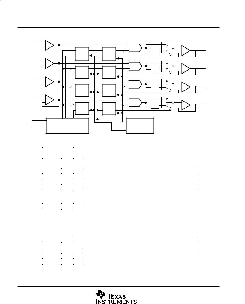
functional block diagram
REFA |
2 |
|
|
+ |
|
|
|
|
± |
|
|
|
8 |
|
Latch |
|
|
|
|
REFB |
3 |
|
|
+ |
|
|
|
|
± |
|
|
|
|
8 |
Latch |
|
|
|
|
REFC |
4 |
|
|
+ |
|
|
|
|
± |
|
|
|
|
8 |
Latch |
|
|
|
|
REFD |
5 |
|
|
+ |
|
|
|
|
± |
|
|
|
|
8 |
Latch |
|
|
|
CLK |
7 |
|
|
6 |
Serial |
||
DATA |
|||
8 |
Interface |
||
LOAD |
|||
|
|||
|
|
Latch |
Latch |
Latch |
Latch |
13 LDAC
|
DAC |
+ |
12 |
DACA |
8 |
× 2 |
± |
|
|
|
|
|
||
|
DAC |
+ |
11 |
DACB |
8 |
× 2 |
± |
|
|
|
|
|||
|
|
|
||
|
DAC |
+ |
10 |
DACC |
8 |
× 2 |
± |
|
|
|
|
|||
|
DAC |
+ |
9 |
DACD |
8 |
× 2 |
± |
|
|
|
|
|
||
|
Power-On |
|
|
|
|
Reset |
|
|
|
|
|
|
Terminal Functions |
|
|
|
|
||
TERMINAL |
I/O |
DESCRIPTION |
||
NAME |
NO. |
|||
|
|
|||
|
|
|
|
|
CLK |
7 |
I |
Serial interface clock. The input digital data is shifted into the serial interface |
|
|
|
|
register on the falling edge of the clock applied to the CLK terminal. |
|
|
|
|
|
|
DACA |
12 |
O |
DAC A analog output |
|
|
|
|
|
|
DACB |
11 |
O |
DAC B analog output |
|
|
|
|
|
|
DACC |
10 |
O |
DAC C analog output |
|
|
|
|
|
|
DACD |
9 |
O |
DAC D analog output |
|
|
|
|
|
|
DATA |
6 |
I |
Serial interface digital data input. The digital code for the DAC is clocked into the |
|
|
|
|
serial interface register serially. Each data bit is clocked into the register on the |
|
|
|
|
falling edge of the clock signal. |
|
|
|
|
|
|
GND |
1 |
I |
Ground return and reference terminal |
|
|
|
|
|
|
LDAC |
13 |
I |
Load DAC. When the LDAC signal is high, no DAC output updates occur when |
|
|
|
|
the input digital data is read into the serial interface. The DAC outputs are only |
|
|
|
|
updated when LDAC is taken from high to low. |
|
|
|
|
|
|
LOAD |
8 |
I |
Serial Interface load control. When LDAC is low, the falling edge of the LOAD |
|
|
|
|
signal latches the digital data into the output latch and immediately produces the |
|
|
|
|
analog voltage at the DAC output terminal. |
|
|
|
|
|
|
REFA |
2 |
I |
Reference voltage input to DAC A. This voltage defines the output analog range. |
|
|
|
|
|
|
REFB |
3 |
I |
Reference voltage input to DAC B. This voltage defines the output analog range. |
|
|
|
|
|
|
REFC |
4 |
I |
Reference voltage input to DAC C. This voltage defines the output analog range. |
|
|
|
|
|
|
REFD |
5 |
I |
Reference voltage input to DAC D. This voltage defines the output analog range. |
|
|
|
|
|
|
VDD |
14 |
I |
Positive supply voltage |
|
2 |
POST OFFICE BOX 655303 •DALLAS, TEXAS 75265 |
TLC5620C, TLC5620I
QUADRUPLE 8-BIT DIGITAL-TO-ANALOG CONVERTERS
SLAS081D ± NOVEMBER 1994 ± REVISED APRIL 1997
detailed description
The TLC5620 is implemented using four resistor-string DACs. The core of each DAC is a single resistor with 256 taps, corresponding to the 256 possible codes listed in Table 1. One end of each resistor string is connected to the GND terminal and the other end is fed from the output of the reference input buffer. Monotonicity is maintained by use of the resistor strings. Linearity depends upon the matching of the resistor elements and upon the performance of the output buffer. Since the inputs are buffered, the DACs always present a high-impedance load to the reference source.
Each DAC output is buffered by a configurable-gain output amplifier that can be programmed to times 1 or times 2 gain.
On power up, the DACs are reset to CODE 0.
Each output voltage is given by: |
|
|
VO(DACA|B|C|D) + REF |
CODE |
(1 )RNG bit value) |
256 |
where CODE is in the range 0 to 255 and the range (RNG) bit is 0 or 1 within the serial control word.
Table 1. Ideal Output Transfer
D7 |
D6 |
D5 |
D4 |
D3 |
D2 |
D1 |
D0 |
OUTPUT VOLTAGE |
|
|
|
|
|
|
|
|
|
0 |
0 |
0 |
0 |
0 |
0 |
0 |
0 |
GND |
0 |
0 |
0 |
0 |
0 |
0 |
0 |
1 |
(1/256) × REF (1+RNG) |
• |
• |
• |
• |
• |
• |
• |
• |
• |
• |
• |
• |
• |
• |
• |
• |
• |
• |
0 |
1 |
1 |
1 |
1 |
1 |
1 |
1 |
(127/256) × REF (1+RNG) |
1 |
0 |
0 |
0 |
0 |
0 |
0 |
0 |
(128/256) × REF (1+RNG) |
• |
• |
• |
• |
• |
• |
• |
• |
• |
• |
• |
• |
• |
• |
• |
• |
• |
• |
1 |
1 |
1 |
1 |
1 |
1 |
1 |
1 |
(255/256) × REF (1+RNG) |
|
|
|
|
|
|
|
|
|
data interface
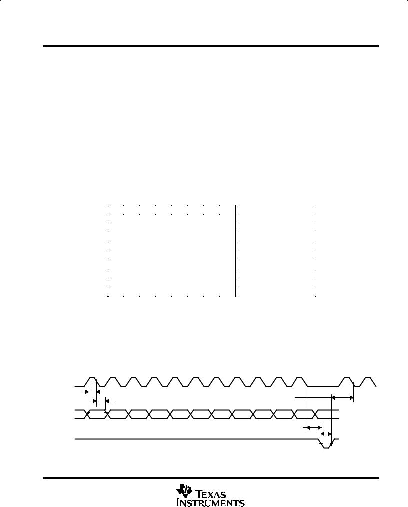
With LOAD high, data is clocked into the DATA terminal on each falling edge of CLK. Once all data bits have been clocked in, LOAD is pulsed low to transfer the data from the serial input register to the selected DAC as shown in Figure 1. When LDAC is low, the selected DAC output voltage is updated when LOAD goes low. When LDAC is high during serial programming, the new value is stored within the device and can be transferred to the DAC output at a later time by pulsing LDAC low as shown in Figure 2. Data is entered most significant bit (MSB) first. Data transfers using two 8-clock cycle periods are shown in Figures 3 and 4.
CLK
DATA
LOAD
tsu(DATA-CLK)
tv(DATA-CLK) tsu(LOAD-CLK)
A1 |
A0 |
RNG |
D7 |
D6 |
D5 |
D4 |
D3 |
D2 |
D1 |
D0 |
|
|
|
|
|
|
|
|
tsu(CLK-LOAD) |
||
tw(LOAD)
DAC Update
Figure 1. LOAD-Controlled Update (LDAC = Low)
POST OFFICE BOX 655303 •DALLAS, TEXAS 75265 |
3 |

TLC5620C, TLC5620I
QUADRUPLE 8-BIT DIGITAL-TO-ANALOG CONVERTERS
SLAS081D ± NOVEMBER 1994 ± REVISED APRIL 1997
CLK
DATA
LOAD
LDAC
 tsu(DATA-CLK)
  tv(DATA-CLK)
A1 A0 RNG D7 D6 D5 D4 D3 D2 D1 D0
tsu(LOAD-LDAC) 
tw(LDAC) 
DAC Update
Figure 2. LDAC-Controlled Update
CLK Low
CLK
DATA A1 A0 RNG
  D7 D6 D5 D4 D3 D2 D1 D0
LOAD
LDAC
Figure 3. Load-Controlled Update Using 8-Bit Serial Word (LDAC = Low)
CLK Low
CLK
DATA A1 A0 RNG
  D7 D6 D5 D4 D3 D2 D1 D0
LOAD
LDAC
Figure 4. LDAC-Controlled Update Using 8-Bit Serial Word
Table 2 lists the A1 and A0 bits and the selection of the updated DACs. The RNG bit controls the DAC output range. When RNG = low, the output range is between the applied reference voltage and GND, and when RNG = high, the range is between twice the applied reference voltage and GND.
Table 2. Serial Input Decode
A1 |
A0 |
DAC UPDATED |
|
|
|
0 |
0 |
DACA |
|
|
|
0 |
1 |
DACB |
|
|
|
1 |
0 |
DACC |
|
|
|
1 |
1 |
DACD |
|
|
|
4 |
POST OFFICE BOX 655303 •DALLAS, TEXAS 75265 |
 Loading...