


Texas Instruments TL5001EVM-101, TL5001EVM-102, TL5001EVM-097, TL5001EVM-089, TL5001EVM-087 Datasheet
...TL5001, TL5001A PULSE-WIDTH-MODULATION CONTROL CIRCUITS
DComplete PWM Power Control
D3.6-V to 40-V Operation
DInternal Undervoltage-Lockout Circuit
DInternal Short-Circuit Protection
DOscillator Frequency . . . 20 kHz to 500 kHz
DVariable Dead Time Provides Control Over Total Range
D±3% Tolerance on Reference Voltage
(TL5001A)
DAvailable in Q-Temp Automotive
HighRel Automotive Applications Configuration Control / Print Support Qualification to Automotive Standards
description
SLVS084E ± APRIL 1994 ± REVISED OCTOBER 1999
D, JG OR P PACKAGE
(TOP VIEW)
|
OUT |
|
1 |
|
8 |
|
|
GND |
|
|
|
|
|
|
|
||||
|
VCC |
|
2 |
|
7 |
|
|
RT |
|
|
|
|
|
|
|
||||
|
COMP |
|
3 |
|
6 |
|
|
DTC |
|
|
|
|
|
|
|
||||
|
FB |
|
4 |
|
5 |
|
|
SCP |
|
|
|
|
|
|
|
||||
|
|
|
|
|
|
|
|
|
|
|
|
|
|
|
|
|
|
|
|
|
|
FK PACKAGE |
|
||||||
|
|
|
(TOP VIEW) |
|
|
||||
|
NC |
|
OUT |
NC |
GND |
NC |
|
||
|
|
|
|
|
|
|
|
|
|
|
3 |
2 |
1 |
20 |
|
19 |
|
||
NC |
4 |
|
|
|
|
|
|
18 |
NC |
VCC |
5 |
|
|
|
|
|
|
17 |
RT |
NC |
6 |
|
|
|
|
|
|
16 |
NC |
The TL5001 and TL5001A incorporate on a single |
COMP |
7 |
|
|
|
|
15 |
DTC |
|
NC |
8 |
|
|
|
|
14 |
NC |
||
monolithic chip all the functions required for a |
|
|
|
|
|||||
|
9 |
10 |
11 |
12 |
13 |
|
|||
pulse-width-modulation (PWM) control circuit. |
|
|
|||||||
|
|
FB |
|
|
|
|
|
|
|
Designed primarily for power-supply control, the |
|
NC |
NC |
SCP |
|
NC |
|
||
TL5001/A contains an error amplifier, a regulator, |
|
|
|
||||||
|
|
|
|
|
|
|
|
|
|
an oscillator, a PWM comparator with a dead-time-control input, undervoltage lockout
(UVLO), short-circuit protection (SCP), and an open-collector output transistor. The TL5001A has a typical reference voltage tolerance of ±3% compared to ±5% for the TL5001.
The error-amplifier common-mode voltage ranges from 0 V to 1.5 V. The noninverting input of the error amplifier is connected to a 1-V reference. Dead-time control (DTC) can be set to provide 0% to 100% dead time by connecting an external resistor between DTC and GND. The oscillator frequency is set by terminating RT with an external resistor to GND. During low VCC conditions, the UVLO circuit turns the output off until VCC recovers to its normal operating range.
The TL5001C and TL5001AC are characterized for operation from ±20°C to 85°C. The TL5001I and TL5001AI are characterized for operation from ±40°C to 85°C. The TL5001Q and TL5001AQ are characterized for operation from ±40°C to 125°C. The TL5001M and TL5001AM are characterized for operation from ±55°C to 125°C.
AVAILABLE OPTIONS
|
|
PACKAGED DEVICES |
|
||
TA |
|
|
|
|
|
SMALL OUTLINE |
PLASTIC DIP |
CERAMIC DIP |
CHIP CARRIER |
||
|
(D) |
(P) |
(JG) |
(FK) |
|
|
|
|
|
|
|
±20°C to 85°C |
TL5001CD |
TL5001CP |
Ð |
Ð |
|
|
|
|
|
||
TL5001ACD |
TL5001ACP |
Ð |
Ð |
||
|
|||||
|
|
|
|
|
|
±40°C to 85°C |
TL5001ID |
TL5001IP |
Ð |
Ð |
|
|
|
|
|
||
TL5001AID |
TL5001AIP |
Ð |
Ð |
||
|
|||||
|
|
|
|
|
|
±40°C to 125°C |
TL5001QD |
Ð |
Ð |
Ð |
|
|
|
|
|
||
TL5001AQD |
Ð |
Ð |
Ð |
||
|
|||||
|
|
|
|
|
|
±55°C to 125°C |
Ð |
Ð |
TL5001MJG |
TL5001MFK |
|
|
|
|
|
||
Ð |
Ð |
TL5001AMJG |
TL5001AMFK |
||
|
|||||
The D package is available taped and reeled. Add the suffix R to the device type (e.g., TL5001CDR).
Please be aware that an important notice concerning availability, standard warranty, and use in critical applications of Texas Instruments semiconductor products and disclaimers thereto appears at the end of this data sheet.
PRODUCTION DATA information is current as of publication date. Products conform to specifications per the terms of Texas Instruments standard warranty. Production processing does not necessarily include testing of all parameters.
Copyright 1999, Texas Instruments Incorporated
POST OFFICE BOX 655303 •DALLAS, TEXAS 75265 |
1 |

TL5001, TL5001A
PULSE-WIDTH-MODULATION CONTROL CIRCUITS
SLVS084E ± APRIL 1994 ± REVISED OCTOBER 1999
schematic for typical application
|
|
|
|
VI |
|
|
|
|
|
|
|
|
|
+ |
|
|
|
|
|
|
|
|
|
TPS1101 |
|
|
|
|
|
|
|
|
|
VO |
|
|
|
|
|
|
|
2 |
+ |
|
|
|
|
|
|
|
VCC |
|
|
|
|
|
|
5 |
SCP |
1 |
|
|
|
|
|
|
|
VO |
|
|
|
|
|
|
|
|
|
COMP 3 |
|
|
|
|
|
|
6 |
TL5001/A |
|
|
|
|
|
|
|
DTC |
|
|
|
|
|
|
|
|
|
4 |
|
|
|
|
|
|
|
|
|
|
|
|
|
|
|
|
7 |
RT |
FB |
|
|
|
|
|
|
|
|
|
||
|
|
|
|
|
|
|
|
|
|
|
|
|
|
|
GND |
|
|
|
|
|
|
|
|
8 |
|
|
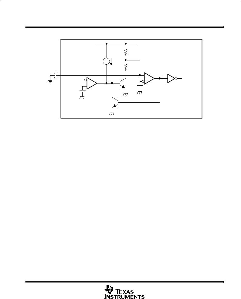
functional block diagram |
|
|
|
|
|
|||
|
|
|
|
VCC |
RT |
DTC |
OUT |
|
|
|
|
|
|
2 |
7 |
6 |
1 |
|
|
|
|
|
|
UVLO |
|
|
|
|
|
|
|
|
IDT |
|
|
|
|
|
1 V |
Reference |
2.5 V |
|
|
|
|
|
|
1.5 V |
1 V |
|
|
||
|
|
|
Voltage |
|
|
|||
|
|
Error |
|
SCP |
|
OSC |
PWM/DTC |
|
|
|
|
|
|
Comparator |
|
||
|
|
Amplifier |
Comparator 1 |
|
|
|||
|
|
|
|
|
||||
|
|
+ |
|
|
|
|
|
|
FB |
4 |
± |
|
|
|
|
|
|
|
|
|
|
|
|
|
||
COMP |
3 |
|
|
|
|
|
|
|
|
|
|
|
|
|
|
|
|
|
|
|
|
|
|
SCP |
|
|
|
|
|
|
|
|
Comparator 2 |
|
|
SCP |
5 |
|
|
|
|
|
|
|
|
|
|
|
|
|
|
|
|
|
|
|
|
|
|
|
|
8 |
|
|
|
|
|
|
|
|
GND |
2 |
POST OFFICE BOX 655303 •DALLAS, TEXAS 75265 |

TL5001, TL5001A
PULSE-WIDTH-MODULATION CONTROL CIRCUITS
SLVS084E ± APRIL 1994 ± REVISED OCTOBER 1999
detailed description
voltage reference
A 2.5-V regulator operating from VCC is used to power the internal circuitry of the TL5001 and TL5001A and as a reference for the error amplifier and SCP circuits. A resistive divider provides a 1-V reference for the error amplifier noninverting input which typically is within 2% of nominal over the operating temperature range.
error amplifier
The error amplifier compares a sample of the dc-to-dc converter output voltage to the 1-V reference and generates an error signal for the PWM comparator. The dc-to-dc converter output voltage is set by selecting the error-amplifier gain (see Figure 1), using the following expression:
VO = (1 + R1/R2) (1 V)
|
3 |
COMP |
TL5001/A |
|
Compensation |
|
|||
|
|
|
||
Network |
|
|
|
|
R1 |
4 |
FB |
± |
|
VI(FB) |
||||
|
|
|||
|
|
|
To PWM |
|
R2 |
|
|
Comparator |
|
|
|
+ |
||
|
|
|
||
|
8 |
GND |
Vref = 1 V |
|
|
|
Figure 1. Error-Amplifier Gain Setting
The error-amplifier output is brought out as COMP for use in compensating the dc-to-dc converter control loop for stability. Because the amplifier can only source 45 µA, the total dc load resistance should be 100 kΩ or more.
oscillator/PWM
The oscillator frequency (fosc) can be set between 20 kHz and 500 kHz by connecting a resistor between RT and GND. Acceptable resistor values range from 15 kΩ to 250 kΩ. The oscillator frequency can be determined
by using the graph shown in Figure 5.
The oscillator output is a triangular wave with a minimum value of approximately 0.7 V and a maximum value of approximately 1.3 V. The PWM comparator compares the error-amplifier output voltage and the DTC input voltage to the triangular wave and turns the output transistor off whenever the triangular wave is greater than the lesser of the two inputs.
dead-time control (DTC)
DTC provides a means of limiting the output-switch duty cycle to a value less than 100%, which is critical for boost and flyback converters. A current source generates a reference current (IDT) at DTC that is nominally equal to the current at the oscillator timing terminal, RT. Connecting a resistor between DTC and GND generates a dead-time reference voltage (VDT), which the PWM/DTC comparator compares to the oscillator triangle wave as described in the previous section. Nominally, the maximum duty cycle is 0% when VDT is 0.7 V or less and 100% when VDT is 1.3 V or greater. Because the triangle wave amplitude is a function of frequency and the source impedance of RT is relatively high (1250 Ω), choosing RDT for a specific maximum duty cycle, D, is accomplished using the following equation and the voltage limits for the frequency in question as found in Figure 11 (Voscmax and Voscmin are the maximum and minimum oscillator levels):
POST OFFICE BOX 655303 •DALLAS, TEXAS 75265 |
3 |
TL5001, TL5001A
PULSE-WIDTH-MODULATION CONTROL CIRCUITS
SLVS084E ± APRIL 1994 ± REVISED OCTOBER 1999
dead-time control (DTC) (continued)
RDT + Rt ) 1250 D Voscmax ± Voscmin ) Voscmin
Where
RDT and Rt are in ohms, D in decimal
Soft start can be implemented by paralleling the DTC resistor with a capacitor (CDT) as shown in Figure 2. During soft start, the voltage at DTC is derived by the following equation:
V |
DT [ |
I |
DT |
R |
DT |
1±e ±t RDTCDT |
|||||||||||||
|
|
|
|
|
|
|
|
|
|
|
|
|
|
|
|
|
|||
|
|
|
|
|
|
|
|
|
|
|
|
|
|
|
|
|
|
|
|
|
|
|
|
|
|
|
|
|
|
|
|
|
|
|
|
|
6 |
DTC |
|
|
|
|
|
|
|
CDT |
|
|
|
|
|
|
|
|
|
|
|
RDT |
TL5001/A |
|
|
|
|
|
|
|
|
|
|
|
|
|
|
|
|
|
|
||
|
|
|
|
|
|
|
|
|
|
|
|
|
|
|
|||||
|
|
|
|
|
|
|
|
|
|
|
|
|
|
|
|
|
|
|
|
|
|
|
|
|
|
|
|
|
|
|
|
|
|
|
|
|
|
|
|
Figure 2. Soft-Start Circuit
If the dc-to-dc converter must be in regulation within a specified period of time, the time constant, RDTCDT, should be t0/3 to t0/5. The TL5001/A remains off until VDT ≈ 0.7 V, the minimum ramp value. CDT is discharged every time UVLO or SCP becomes active.
undervoltage-lockout (UVLO) protection
The undervoltage-lockout circuit turns the output transistor off and resets the SCP latch whenever the supply voltage drops too low (approximately 3 V at 25°C) for proper operation. A hysteresis voltage of 200 mV eliminates false triggering on noise and chattering.
short-circuit protection (SCP)
The TL5001/A includes short-circuit protection (see Figure 3), which turns the power switch off to prevent damage when the converter output is shorted. When activated, the SCP prevents the switch from being turned on until the internal latching circuit is reset. The circuit is reset by reducing the input voltage until UVLO becomes active or until the SCP terminal is pulled to ground externally.
When a short circuit occurs, the error-amplifier output at COMP rises to increase the power-switch duty cycle in an attempt to maintain the output voltage. SCP comparator 1 starts an RC timing circuit when COMP exceeds 1.5 V. If the short is removed and the error-amplifier output drops below 1.5 V before time out, normal converter operation continues. If the fault is still present at the end of the time-out period, the timer sets the latching circuit and turns off the TL5001/A output transistor.
4 |
POST OFFICE BOX 655303 •DALLAS, TEXAS 75265 |
TL5001, TL5001A
PULSE-WIDTH-MODULATION CONTROL CIRCUITS
|
|
|
|
SLVS084E ± APRIL 1994 ± REVISED OCTOBER 1999 |
short-circuit protection (SCP) (continued) |
|
|
||
|
|
2.5 V |
|
|
|
|
RSCP |
185 kΩ |
|
CSCP |
|
|
12 kΩ |
SCP |
SCP |
|
|
Comparator 2 |
|
|
|
|
To Output |
|
5 |
From Error |
|
|
|
|
|
|
Drive Logic |
|
|
Amp |
|
Q1 |
|
|
|
|
||
|
|
SCP |
|
Vref = 1 V |
|
1.5 V |
|
|
|
|
Comparator 1 |
|
|
|
|
|
|
|
|
|
|
Q2 |
|
|
Figure 3. SCP Circuit
The timer operates by charging an external capacitor (CSCP), connected between the SCP terminal and ground, towards 2.5 V through a 185-kΩ resistor (RSCP). The circuit begins charging from an initial voltage of approximately 185 mV and times out when the capacitor voltage reaches 1 V. The output of SCP comparator 2 then goes high, turns on Q2, and latches the timer circuit. The expression for setting the SCP time period is derived from the following equation:
VSCP + (2.5 * 0.185) 1 * e±t t ) 0.185
Where
τ = RSCPCSCP
The end of the time-out period, tSCP, occurs when VSCP = 1 V. Solving for CSCP yields:
CSCP + 12.46 tSCP
Where
t is in seconds, C in µF.
tSCP must be much longer (generally 10 to 15 times) than the converter start-up period or the converter will not start.
output transistor
The output of the TL5001/A is an open-collector transistor with a maximum collector current rating of 21 mA and a voltage rating of 51 V. The output is turned on under the following conditions: the oscillator triangle wave is lower than both the DTC voltage and the error-amplifier output voltage, the UVLO circuit is inactive, and the short-circuit protection circuit is inactive.
POST OFFICE BOX 655303 •DALLAS, TEXAS 75265 |
5 |

TL5001, TL5001A
PULSE-WIDTH-MODULATION CONTROL CIRCUITS
SLVS084E ± APRIL 1994 ± REVISED OCTOBER 1999
absolute maximum ratings over operating free-air temperature range (unless otherwise noted)²
Supply voltage, VCC (see Note 1) . . . . . . . . . . . . . . . . . . . . . . . . . . . . . . . . . . . . . . . |
. . . . . . . . . . . . . . . . . . . . . 41 V |
Amplifier input voltage, VI(FB) . . . . . . . . . . . . . . . . . . . . . . . . . . . . . . . . . . . . . . . . . . |
. . . . . . . . . . . . . . . . . . . . . 20 V |
Output voltage, VO, OUT . . . . . . . . . . . . . . . . . . . . . . . . . . . . . . . . . . . . . . . . . . . . . . |
. . . . . . . . . . . . . . . . . . . . . 51 V |
Output current, IO, OUT . . . . . . . . . . . . . . . . . . . . . . . . . . . . . . . . . . . . . . . . . . . . . . . |
. . . . . . . . . . . . . . . . . . . 21 mA |
Output peak current, IO(peak), OUT . . . . . . . . . . . . . . . . . . . . . . . . . . . . . . . . . . . . . |
. . . . . . . . . . . . . . . . . . 100 mA |
Continuous total power dissipation . . . . . . . . . . . . . . . . . . . . . . . . . . . . . . . . . . . . . |
See Dissipation Rating Table |
Operating ambient temperature range, TA: TL5001C, TL5001AC . . . . . . . . . . |
. . . . . . . . . . . . ±20°C to 85°C |
TL5001I, TL5001AI . . . . . . . . . . . . |
. . . . . . . . . . . . ±40°C to 85°C |
TL5001Q, TL5001AQ . . . . . . . . . . |
. . . . . . . . . . . ±40°C to 125°C |
TL5001M, TL5001AM . . . . . . . . . . |
. . . . . . . . . . . ±55°C to 125°C |
Storage temperature range, Tstg . . . . . . . . . . . . . . . . . . . . . . . . . . . . . . . . . . . . . . . . |
. . . . . . . . . . . ±65°C to 150°C |
Lead temperature 1,6 mm (1/16 inch) from case for 10 seconds . . . . . . . . . . . . |
. . . . . . . . . . . . . . . . . . . 260°C |
²Stresses beyond those listed under ªabsolute maximum ratingsº may cause permanent damage to the device. These are stress ratings only, and functional operation of the device at these or any other conditions beyond those indicated under ªrecommended operating conditionsº is not implied. Exposure to absolute-maximum-rated conditions for extended periods may affect device reliability.
NOTE 1: All voltage values are with respect to network ground terminal.
DISSIPATION RATING TABLE
PACKAGE |
TA ≤ 25°C |
DERATING FACTOR |
TA = 70°C |
TA = 85°C |
TA = 125°C |
|
POWER RATING |
ABOVE TA = 25°C |
POWER RATING |
POWER RATING |
POWER RATING |
||
|
||||||
D |
725 mW |
5.8 mW/°C |
464 mW |
377 mW |
145 mW |
|
FK |
1375 mW |
11.0 mW/°C |
880 mW |
715 mW |
275 mW |
|
JG |
1050 mW |
8.4 mW/°C |
672 mW |
546 mW |
210 mW |
|
P |
1000 mW |
8.0 mW/°C |
640 mW |
520 mW |
200 mW |
|
|
|
|
|
|
|
recommended operating conditions
|
|
MIN |
MAX |
UNIT |
|
|
|
|
|
|
|
Supply voltage, VCC |
|
3.6 |
40 |
V |
|
Amplifier input voltage, VI(FB) |
|
0 |
1.5 |
V |
|
Output voltage, VO, OUT |
|
|
50 |
V |
|
Output current, IO, OUT |
|
|
20 |
mA |
|
COMP source current |
|
|
45 |
µA |
|
COMP dc load resistance |
|
100 |
|
kΩ |
|
|
|
|
|
|
|
Oscillator timing resistor, Rt |
|
15 |
250 |
kΩ |
|
Oscillator frequency, fosc |
|
20 |
500 |
kHz |
|
|
TL5001C, TL5001AC |
± 20 |
85 |
|
|
|
|
|
|
|
|
Operating ambient temperature, TA |
TL5001I, TL5001AI |
± 40 |
85 |
°C |
|
|
|
|
|||
TL5001Q, TL5001AQ |
± 40 |
125 |
|||
|
|
||||
|
|
|
|
|
|
|
TL5001M, TL5001AM |
± 55 |
125 |
|
6 |
POST OFFICE BOX 655303 •DALLAS, TEXAS 75265 |
TL5001, TL5001A
PULSE-WIDTH-MODULATION CONTROL CIRCUITS
SLVS084E ± APRIL 1994 ± REVISED OCTOBER 1999
electrical characteristics over recommended operating free-air temperature range, VCC = 6 V, fosc = 100 kHz (unless otherwise noted)
reference
PARAMETER |
TEST CONDITIONS |
TL5001C, TL5001I |
TL5001AC, TL5001AI |
UNIT |
|||||
|
|
|
|
|
|
||||
MIN |
TYP² |
MAX |
MIN |
TYP² |
MAX |
||||
|
|
|
|||||||
Output voltage |
COMP connected to FB |
0.95 |
1 |
1.05 |
0.97 |
1 |
1.03 |
V |
|
|
|
|
|
|
|
|
|
|
|
Input regulation |
VCC = 3.6 V to 40 V |
|
2 |
12.5 |
|
2 |
12.5 |
mV |
|
|
TA = ± 20°C to 25°C (C suffix) |
± 10 |
± 1 |
10 |
± 10 |
± 1 |
10 |
|
|
Output voltage change with temperature |
TA = ± 40°C to 25°C (I suffix) |
± 10 |
± 1 |
10 |
± 10 |
± 1 |
10 |
mV/V |
|
|
TA = 25°C to 85°C |
± 10 |
± 2 |
10 |
± 10 |
± 2 |
10 |
|
|
² All typical values are at T = 25°C. |
|
|
|
|
|
|
|
|
|
A |
|
|
|
|
|
|
|
|
|
undervoltage lockout |
|
|
|
|
|
|
|
|
|
PARAMETER |
TEST CONDITIONS |
TL5001C, TL5001I |
TL5001AC, TL5001AI |
UNIT |
||||
|
|
|
|
|
||||
MIN |
TYP² MAX |
MIN |
TYP² |
MAX |
||||
|
|
|
||||||
Upper threshold voltage |
TA = 25°C |
|
3 |
|
3 |
|
V |
|
Lower threshold voltage |
TA = 25°C |
|
2.8 |
|
2.8 |
|
V |
|
Hysteresis |
TA = 25°C |
100 |
200 |
100 |
200 |
|
mV |
|
Reset threshold voltage |
TA = 25°C |
2.1 |
2.55 |
2.1 |
2.55 |
|
V |
|
² All typical values are at T = 25°C. |
|
|
|
|
|
|
|
|
A |
|
|
|
|
|
|
|
|
short-circuit protection |
|
|
|
|
|
|
|
|
PARAMETER |
TEST CONDITIONS |
TL5001C, TL5001I |
TL5001AC, TL5001AI |
UNIT |
|||||
|
|
|
|
|
|
||||
MIN |
TYP² |
MAX |
MIN |
TYP² |
MAX |
||||
|
|
|
|||||||
SCP threshold voltage |
TA = 25°C |
0.95 |
1.00 |
1.05 |
0.97 |
1.00 |
1.03 |
V |
|
SCP voltage, latched |
No pullup |
140 |
185 |
230 |
140 |
185 |
230 |
mV |
|
|
|
|
|
|
|
|
|
|
|
SCP voltage, UVLO standby |
No pullup |
|
60 |
120 |
|
60 |
120 |
mV |
|
|
|
|
|
|
|
|
|
|
|
Input source current |
TA = 25°C |
±10 |
±15 |
±20 |
±10 |
±15 |
±20 |
µA |
|
SCP comparator 1 threshold voltage |
|
|
1.5 |
|
|
1.5 |
|
V |
|
|
|
|
|
|
|
|
|
|
|
² All typical values are at T = 25°C. |
|
|
|
|
|
|
|
|
|
A |
|
|
|
|
|
|
|
|
|
oscillator |
|
|
|
|
|
|
|
|
|
PARAMETER |
TEST CONDITIONS |
TL5001C, TL5001I |
TL5001AC, TL5001AI |
UNIT |
|||||
|
|
|
|
|
|
||||
MIN |
TYP² |
MAX |
MIN |
TYP² |
MAX |
||||
|
|
|
|||||||
Frequency |
Rt = 100 kΩ |
|
100 |
|
|
100 |
|
kHz |
|
Standard deviation of frequency |
|
|
15 |
|
|
15 |
|
kHz |
|
|
|
|
|
|
|
|
|
|
|
Frequency change with voltage |
VCC = 3.6 V to 40 V |
|
1 |
|
|
1 |
|
kHz |
|
|
TA = ± 40°C to 25°C |
± 4 |
± 0.4 |
4 |
± 4 |
± 0.4 |
4 |
kHz |
|
Frequency change with temperature |
TA = ± 20°C to 25°C |
± 4 |
± 0.4 |
4 |
± 4 |
± 0.4 |
4 |
kHz |
|
|
TA = 25°C to 85°C |
± 4 |
± 0.2 |
4 |
± 4 |
± 0.2 |
4 |
kHz |
|
Voltage at RT |
|
|
1 |
|
|
1 |
|
V |
|
|
|
|
|
|
|
|
|
|
|
² All typical values are at T = 25°C. |
|
|
|
|
|
|
|
|
|
A |
|
|
|
|
|
|
|
|
|
POST OFFICE BOX 655303 •DALLAS, TEXAS 75265 |
7 |
 Loading...