


Texas Instruments TLC3704MJB, TLC3704MFKB, TLC3704MJ, TLC3704MD, TLC3704IPWR Datasheet
...QUAD MICROPOWER LinCMOS |
|
|
TLC3704, TLC3704Q |
||||
VOLTAGE COMPARATORS |
|||||||
|
SLCS117A ± NOVEMBER 1986 ± REVISED OCTOBER 1996 |
||||||
|
|
|
|
|
|
|
|
D Push-Pull CMOS Output Drives Capacitive |
D, J, OR N PACKAGE |
||||||
Loads Without Pullup Resistor, |
|
(TOP VIEW) |
|
|
|
||
IO = ± 8 mA |
1OUT |
|
|
|
|
3OUT |
|
|
1 |
14 |
|
||||
|
|
||||||
D Very Low Power . . . 200 μW Typ at 5 V |
|
|
|||||
2OUT |
|
2 |
13 |
|
4OUT |
||
|
|
||||||
D Fast Response Time . . . tPLH = 2.7 μs Typ |
|
|
|||||
VDD |
|
3 |
12 |
|
GND |
||
|
|
||||||
With 5-mV Overdrive |
2IN ± |
|
4 |
11 |
|
4IN + |
|
|
|
||||||
D Single Supply Operation . . . 3 V to 16 V |
2IN + |
|
5 |
10 |
|
4IN ± |
|
TLC3704M . . . 4 V to 16 V |
1IN ± |
|
6 |
9 |
|
3IN + |
|
D On-Chip ESD Protection |
1IN + |
|
7 |
8 |
|
3IN ± |
|
|
|
|
|
|
|
|
|
description
The TLC3704 consists of four independent micropower voltage comparators designed to operate from a single supply and be compatible with modern HCMOS logic systems. They are functionally similar to the LM339 but use 1/20th the power for similar response times. The push-pull CMOS output stage drives capacitive loads directly without a power-consuming pullup resistor to achieve the stated response time. Eliminating the pullup resistor not only reduces power dissipation, but also saves board space and component cost. The output stage is also fully compatible with TTL requirements.
Texas Instruments LinCMOS process offers superior analog performance to standard CMOS processes. Along with the standard CMOS advantages of low power without sacrificing speed, high input impedance, and low bias currents, the LinCMOS process offers extremely stable input offset voltages with large differential input voltages. This characteristic makes it possible to build reliable CMOS comparators.
FK PACKAGE (TOP VIEW)
|
2OUT |
1OUT |
NC |
3OUT |
4OUT |
|
VDD |
3 |
2 |
1 |
20 19 |
GND |
|
4 |
|
|
|
18 |
||
NC |
5 |
|
|
|
17 |
NC |
2IN ± |
6 |
|
|
|
16 |
4IN + |
NC |
7 |
|
|
|
15 |
NC |
2IN + |
8 |
|
|
|
14 |
4IN ± |
|
9 |
10 11 12 13 |
|
|||
|
1IN± |
1IN+ |
NC |
3IN± |
3IN+ |
|
NC ± No internal connection
symbol (each comparator)
IN +
OUT
IN ±
The TLC3704C is characterized for operation over the commercial temperature range of 0°C to 70°C. The TLC3704I is characterized for operation over the extended industrial temperature range of ± 40°C to 85°C. The TLC3704M is characterized for operation over the full military temperature range of ± 55°C to 125°C. The TLC3704Q is characterized for operation from ± 40°C to 125°C.
Please be aware that an important notice concerning availability, standard warranty, and use in critical applications of Texas Instruments semiconductor products and disclaimers thereto appears at the end of this data sheet.
LinCMOS is a trademark of Texas Instruments Incorporated.
PRODUCTION DATA information is current as of publication date. Products conform to specifications per the terms of Texas Instruments standard warranty. Production processing does not necessarily include testing of all parameters.
Copyright 1996, Texas Instruments Incorporated
POST OFFICE BOX 655303 •DALLAS, TEXAS 75265 |
1 |
TLC3704, TLC3704Q
QUAD MICROPOWER LinCMOS VOLTAGE COMPARATORS
SLCS117A ± NOVEMBER 1986 ± REVISED OCTOBER 1996
AVAILABLE OPTIONS
|
VIOmax |
|
PACKAGE |
|
||
TA |
|
|
|
|
||
SMALL OUTLINE |
CERAMIC |
CERAMIC DIP |
PLASTIC DIP |
|||
at 25°C |
||||||
|
(D) |
(FK) |
(J) |
(N) |
||
|
|
|||||
|
|
|
|
|
|
|
0°C to 70°C |
5 mV |
TLC3704CD |
Ð |
Ð |
TLC3704CN |
|
|
|
|
|
|
|
|
± 40°C to 85°C |
5 mV |
TLC3704ID |
Ð |
Ð |
TLC3704IN |
|
|
|
|
|
|
|
|
± 55°C to 125°C |
5 mV |
Ð |
TLC3704MFK |
TLC3704MJ |
Ð |
|
|
|
|
|
|
|
|
± 40°C to 125°C |
5 mV |
Ð |
Ð |
TLC3704QJ |
Ð |
|
|
|
|
|
|
|
|
The D package is available taped and reeled. Add R suffix to the device type (e.g., TLC3704CDR).
functional block diagram (each comparator)
VDD
IN+
Differential
Input 
 OUT
OUT
Circuits
IN±
GND
absolute maximum ratings over operating free-air temperature range (unless otherwise noted)²
Supply voltage range, VDD (see Note 1) . . . . . . . . . . . . . . . . . . . . . . . . . . . . . . . . . |
. . . . . . . . . . . |
. ± 0.3 V to 18 V |
Differential input voltage, VID (see Note 2) . . . . . . . . . . . . . . . . . . . . . . . . . . . . . . . |
. . . . . . . . . . . . |
. . . . . . . ± 18 V |
Input voltage range, VI . . . . . . . . . . . . . . . . . . . . . . . . . . . . . . . . . . . . . . . . . . . . . . . . . |
. . . . . . . . . . . . |
. . ± 0.3 to VDD |
Output voltage range, VO . . . . . . . . . . . . . . . . . . . . . . . . . . . . . . . . . . . . . . . . . . . . . . |
. . . . . . . . . . . . |
. . ± 0.3 to VDD |
Input current, II . . . . . . . . . . . . . . . . . . . . . . . . . . . . . . . . . . . . . . . . . . . . . . . . . . . . . . . |
. . . . . . . . . . . . |
. . . . . . . ± 5 mA |
Output current, IO (each output) . . . . . . . . . . . . . . . . . . . . . . . . . . . . . . . . . . . . . . . . |
. . . . . . . . . . . . |
. . . . . . ± 20 mA |
Total supply current into VDD . . . . . . . . . . . . . . . . . . . . . . . . . . . . . . . . . . . . . . . . . . . |
. . . . . . . . . . . . |
. . . . . . . 40 mA |
Total current out of GND . . . . . . . . . . . . . . . . . . . . . . . . . . . . . . . . . . . . . . . . . . . . . . . |
. . . . . . . . . . . . |
. . . . . . . 60 mA |
Continuous total power dissipation . . . . . . . . . . . . . . . . . . . . . . . . . . . . . . . . . . . . . |
See Dissipation Rating Table |
|
Operating free-air temperature range, TA: TLC3704C . . . . . . . . . . . . . . . . . . . . . . |
. . . . . . . . . . . . |
. . . . . 0 to 70°C |
TLC3704I . . . . . . . . . . . . . . . . . . . . . . . |
. . . . . . . . . . . . |
± 40°C to 85°C |
TLC3704M . . . . . . . . . . . . . . . . . . . . . . |
. . . . . . . . . . |
± 55°C to 125°C |
TLC3704Q . . . . . . . . . . . . . . . . . . . . . . |
. . . . . . . . . . |
± 40°C to 125°C |
Storage temperature range . . . . . . . . . . . . . . . . . . . . . . . . . . . . . . . . . . . . . . . . . . . . . |
. . . . . . . . . . |
± 65°C to 150°C |
Case temperature for 60 seconds: FK package . . . . . . . . . . . . . . . . . . . . . . . . . . . |
. . . . . . . . . . . . |
. . . . . . . 260°C |
Lead temperature 1,6 mm (1/16 inch) from case for 10 seconds: D or N package . . . . . . . . . |
. . . . . . . 260°C |
|
Lead temperature 1,6 mm (1/16 inch) from case for 60 seconds: J package . . |
. . . . . . . . . . . . |
. . . . . . . 300°C |
²Stresses beyond those listed under ªabsolute maximum ratingsº may cause permanent damage to the device. These are stress ratings only, and functional operation of the device at these or any other conditions beyond those indicated under ªrecommended operating conditionsº is not
implied. Exposure to absolute-maximum-rated conditions for extended periods may affect device reliability. NOTES: 1. All voltage values, except differential voltages, are with respect to network ground.
2. Differential voltages are at IN+ with respect to IN ±.
2 |
POST OFFICE BOX 655303 •DALLAS, TEXAS 75265 |

|
|
|
QUAD MICROPOWER LinCMOS |
TLC3704, TLC3704Q |
|||||
|
|
|
VOLTAGE COMPARATORS |
||||||
|
|
|
|
SLCS117A ± NOVEMBER 1986 ± REVISED OCTOBER 1996 |
|||||
|
|
|
|
|
|
|
|
|
|
|
|
|
DISSIPATION RATING TABLE |
|
|
|
|
|
|
|
|
|
|
|
|
|
|
||
|
PACKAGE |
TA ≤ 25°C |
DERATING FACTOR |
TA = 70°C |
TA = 85°C |
TA = 125°C |
|
||
|
POWER RATING |
ABOVE TA = 25°C |
POWER RATING |
POWER RATING |
POWER RATING |
|
|
||
|
|
|
|||||||
|
D |
950 mW |
7.6 mW/°C |
608 mW |
|
494 mW |
N/A |
|
|
|
FK |
1375 mW |
11.0 mW/°C |
880 mW |
|
715 mW |
275 mW |
|
|
|
J |
1375 mW |
11.0 mW/°C |
880 mW |
|
715 mW |
275 mW |
|
|
|
N |
1150 mW |
9.2 mW/°C |
736 mW |
|
598 mW |
N/A |
|
|
|
|
|
|
|
|
|
|
|
|
recommended operating conditions
|
|
TLC3704C |
UNIT |
|
|
|
|
|
|
|
MIN |
NOM |
MAX |
|
|
|
|||
|
|
|
|
|
Supply voltage, VDD |
3 |
5 |
16 |
V |
Common-mode input voltage, VIC |
± 0.2 |
|
VDD ± 1.5 |
V |
High-level output current, IOH |
|
|
± 20 |
mA |
Low-level output current, IOL |
|
|
20 |
mA |
Operating free-air temperature, TA |
0 |
|
70 |
°C |
electrical characteristics at specified operating free-air temperature, VDD = 5 V (unless otherwise noted)
|
PARAMETER |
TEST CONDITIONS² |
TA |
TLC3704C |
|
UNIT |
||
|
|
|
|
|||||
|
MIN |
TYP |
MAX |
|||||
|
|
|
|
|
|
|||
|
|
|
|
|
|
|
|
|
VIO |
Input offset voltage |
VDD = 5 V to 10 V, |
25°C |
|
1.2 |
5 |
mV |
|
VIC = VICRmin, |
See Note 3 |
0°C to 70°C |
|
|
6.5 |
|||
|
|
|
|
|
||||
IIO |
Input offset current |
VIC = 2.5 V |
|
25°C |
|
1 |
|
pA |
|
|
|
|
|
|
|||
|
70°C |
|
|
0.3 |
nA |
|||
|
|
|
|
|
|
|||
|
|
|
|
|
|
|
|
|
IIB |
Input bias current |
VIC = 2.5 V |
|
25°C |
|
5 |
|
pA |
|
|
|
|
|
|
|||
|
70°C |
|
|
0.6 |
nA |
|||
|
|
|
|
|
|
|||
|
|
|
|
|
|
|
|
|
|
|
|
|
25°C |
0 to |
|
|
|
|
|
|
|
VDD ± 1 |
|
|
|
|
VICR |
Common-mode input voltage range |
|
|
|
|
|
V |
|
|
|
0°C to 70°C |
0 to |
|
|
|||
|
|
|
|
|
|
|
||
|
|
|
|
VDD ± 1.5 |
|
|
|
|
|
|
|
|
|
|
|
|
|
|
|
|
|
25°C |
|
84 |
|
|
|
|
|
|
|
|
|
|
|
CMRR |
Common-mode rejection ratio |
VIC = VICRmin |
|
70°C |
|
84 |
|
dB |
|
|
|
|
0°C |
|
84 |
|
|
|
|
|
|
|
|
|
|
|
|
|
|
|
25°C |
|
85 |
|
|
|
|
|
|
|
|
|
|
|
kSVR |
Supply-voltage rejection ratio |
VDD = 5 V to 10 V |
|
70°C |
|
85 |
|
dB |
|
|
|
|
0°C |
|
85 |
|
|
|
|
|
|
|
|
|
|
|
VOH |
High-level output voltage |
VID = 1 V, |
IOH = ±4 mA |
25°C |
4.5 |
4.7 |
|
V |
|
|
|
|
|||||
70°C |
4.3 |
|
|
|||||
|
|
|
|
|
|
|
||
|
|
|
|
|
|
|
|
|
VOL |
Low-level output voltage |
VID = ±1 V, |
IOH = 4 mA |
25°C |
|
210 |
300 |
mV |
|
|
|
|
|||||
70°C |
|
|
375 |
|||||
|
|
|
|
|
|
|
||
|
|
|
|
|
|
|
|
|
IDD |
Supply current (all four comparators) |
Outputs low, |
No load |
25°C |
|
35 |
80 |
μA |
|
|
|
|
|||||
0°C to 70°C |
|
|
100 |
|||||
|
|
|
|
|
|
|
||
|
|
|
|
|
|
|
|
|
² All characteristics are measured with zero common-mode voltage unless otherwise noted.
NOTE 3: The offset voltage limits given are the maximum values required to drive the output up to 4.5 V or down to 0.3 V.
POST OFFICE BOX 655303 •DALLAS, TEXAS 75265 |
3 |

TLC3704, TLC3704Q
QUAD MICROPOWER LinCMOS VOLTAGE COMPARATORS
SLCS117A ± NOVEMBER 1986 ± REVISED OCTOBER 1996
recommended operating conditions
|
|
TLC3704I |
UNIT |
|
|
|
|
|
|
|
MIN |
NOM |
MAX |
|
|
|
|||
|
|
|
|
|
Supply voltage, VDD |
3 |
5 |
16 |
V |
Common-mode input voltage, VIC |
± 0.2 |
|
VDD ± 1.5 |
V |
High-level output current, IOH |
|
|
± 20 |
mA |
Low-level output current, IOL |
|
|
20 |
mA |
Operating free-air temperature, TA |
± 40 |
|
85 |
°C |
electrical characteristics at specified operating free-air temperature, VDD = 5 V, VIC = 0 (unless otherwise noted)
|
PARAMETER |
TEST CONDITIONS |
TA |
TLC3704I |
|
UNIT |
||
|
|
|
|
|||||
|
MIN |
TYP |
MAX |
|||||
|
|
|
|
|
|
|||
|
|
|
|
|
|
|
|
|
VIO |
Input offset voltage |
VDD = 5 V to 10 V, |
25°C |
|
1.2 |
5 |
mV |
|
VIC = VICRmin, |
See Note 3 |
± 40°C to 85°C |
|
|
7 |
|||
|
|
|
|
|
||||
IIO |
Input offset current |
VIC = 2.5 V |
|
25°C |
|
1 |
|
pA |
|
|
|
|
|
|
|||
|
85°C |
|
|
1 |
nA |
|||
|
|
|
|
|
|
|||
|
|
|
|
|
|
|
|
|
IIB |
Input bias current |
VIC = 2.5 V |
|
25°C |
|
5 |
|
pA |
|
|
|
|
|
|
|||
|
85°C |
|
|
2 |
nA |
|||
|
|
|
|
|
|
|||
|
|
|
|
|
|
|
|
|
|
|
|
|
25°C |
0 to |
|
|
|
|
|
|
|
VDD ± 1 |
|
|
|
|
VICR |
Common-mode input voltage range |
|
|
|
|
|
V |
|
|
|
± 40°C to 85°C |
0 to |
|
|
|||
|
|
|
|
|
|
|
||
|
|
|
|
VDD ± 1.5 |
|
|
|
|
|
|
|
|
|
|
|
|
|
|
|
|
|
25°C |
|
84 |
|
|
|
|
|
|
|
|
|
|
|
CMRR |
Common-mode rejection ratio |
VIC = VICRmin |
|
85°C |
|
84 |
|
dB |
|
|
|
|
± 40°C |
|
83 |
|
|
|
|
|
|
|
|
|
|
|
|
|
|
|
25°C |
|
85 |
|
|
|
|
|
|
|
|
|
|
|
kSVR |
Supply-voltage rejection ratio |
VDD = 5 V to 10 V |
|
85°C |
|
85 |
|
dB |
|
|
|
|
± 40°C |
|
83 |
|
|
|
|
|
|
|
|
|
|
|
VOH |
High-level output voltage |
VID = 1 V, |
IOH = ±4 mA |
25°C |
4.5 |
4.7 |
|
V |
|
|
|
|
|||||
85°C |
4.3 |
|
|
|||||
|
|
|
|
|
|
|
||
|
|
|
|
|
|
|
|
|
VOL |
Low-level output voltage |
VID = ±1 V, |
IOH = 4 mA |
25°C |
|
210 |
300 |
mV |
|
|
|
|
|||||
85°C |
|
|
400 |
|||||
|
|
|
|
|
|
|
||
|
|
|
|
|
|
|
|
|
IDD |
Supply current (all four comparators) |
Outputs low, |
No load |
25°C |
|
35 |
80 |
μA |
|
|
|
|
|||||
± 40°C to 85°C |
|
|
125 |
|||||
|
|
|
|
|
|
|
||
|
|
|
|
|
|
|
|
|
NOTE 3: The offset voltage limits given are the maximum values required to drive the output up to 4.5 V or down to 0.3 V.
4 |
POST OFFICE BOX 655303 •DALLAS, TEXAS 75265 |
QUAD MICROPOWER LinCMOS |
|
|
TLC3704, TLC3704Q |
|||
VOLTAGE COMPARATORS |
||||||
SLCS117A ± NOVEMBER 1986 ± REVISED OCTOBER 1996 |
||||||
|
|
|
|
|
|
|
recommended operating conditions |
|
|
|
|
|
|
|
|
|
|
|
|
|
|
|
|
TLC3704M |
UNIT |
|
|
|
|
|
|
|
|
|
|
|
MIN |
NOM |
MAX |
|
|
|
|
|
|
|||
|
|
|
|
|
|
|
Supply voltage, VDD |
|
4 |
5 |
16 |
V |
|
Common-mode input voltage, VIC |
|
0 |
|
VDD ± 1.5 |
V |
|
High-level output current, IOH |
|
|
|
± 20 |
mA |
|
Low-level output current, IOL |
|
|
|
20 |
mA |
|
Operating free-air temperature, TA |
|
± 55 |
|
125 |
°C |
|
electrical characteristics at specified operating free-air temperature, VDD = 5 V, VIC = 0 (unless otherwise noted)
|
PARAMETER |
TEST CONDITIONS |
TA |
TLC3704M |
|
UNIT |
||
|
|
|
|
|||||
|
MIN |
TYP |
MAX |
|||||
|
|
|
|
|
|
|||
|
|
|
|
|
|
|
|
|
VIO |
Input offset voltage |
VDD = 5 V to 10 V, |
|
25°C |
|
1.2 |
5 |
mV |
VIC = VICRmin, |
See Note 3 |
± 55°C to 125°C |
|
|
10 |
|||
|
|
|
|
|
||||
IIO |
Input offset current |
VIC = 2.5 V |
|
25°C |
|
1 |
|
pA |
|
|
|
|
|
|
|||
|
125°C |
|
|
15 |
nA |
|||
|
|
|
|
|
|
|||
|
|
|
|
|
|
|
|
|
IIB |
Input bias current |
VIC = 2.5 V |
|
25°C |
|
5 |
|
pA |
|
|
|
|
|
|
|||
|
125°C |
|
|
30 |
nA |
|||
|
|
|
|
|
|
|||
|
|
|
|
|
|
|
|
|
|
|
|
|
25°C |
0 to |
|
|
|
|
|
|
|
VDD ± 1 |
|
|
|
|
VICR |
Common-mode input voltage range |
|
|
|
|
|
V |
|
|
|
± 55°C to 125°C |
0 to |
|
|
|||
|
|
|
|
|
|
|
||
|
|
|
|
VDD ± 1.5 |
|
|
|
|
|
|
|
|
|
|
|
|
|
|
|
|
|
25°C |
|
84 |
|
|
|
|
|
|
|
|
|
|
|
CMRR |
Common-mode rejection ratio |
VIC = VICRmin |
|
125°C |
|
83 |
|
dB |
|
|
|
|
± 55°C |
|
82 |
|
|
|
|
|
|
|
|
|
|
|
|
|
|
|
25°C |
|
85 |
|
|
|
|
|
|
|
|
|
|
|
kSVR |
Supply-voltage rejection ratio |
VDD = 5 V to 10 V |
|
125°C |
|
85 |
|
dB |
|
|
|
|
± 55°C |
|
82 |
|
|
|
|
|
|
|
|
|
|
|
VOH |
High-level output voltage |
VID = 1 V, |
IOH = ±4 mA |
25°C |
4.5 |
4.7 |
|
V |
|
|
|
|
|||||
125°C |
4.2 |
|
|
|||||
|
|
|
|
|
|
|
||
|
|
|
|
|
|
|
|
|
VOL |
Low-level output voltage |
VID = ±1 V, |
IOH = 4 mA |
25°C |
|
210 |
300 |
mV |
|
|
|
|
|||||
125°C |
|
|
500 |
|||||
|
|
|
|
|
|
|
||
|
|
|
|
|
|
|
|
|
IDD |
Supply current (all four comparators) |
Outputs low, |
No load |
25°C |
|
35 |
80 |
μA |
|
|
|
|
|||||
± 55°C to 125°C |
|
|
175 |
|||||
|
|
|
|
|
|
|
||
|
|
|
|
|
|
|
|
|
NOTE 3: The offset voltage limits given are the maximum values required to drive the output up to 4.5 V or down to 0.3 V.
POST OFFICE BOX 655303 •DALLAS, TEXAS 75265 |
5 |

TLC3704, TLC3704Q
QUAD MICROPOWER LinCMOS VOLTAGE COMPARATORS
SLCS117A ± NOVEMBER 1986 ± REVISED OCTOBER 1996
recommended operating conditions
|
|
TLC3704Q |
UNIT |
|
|
|
|
|
|
|
MIN |
NOM |
MAX |
|
|
|
|||
|
|
|
|
|
Supply voltage, VDD |
3 |
5 |
16 |
V |
Common-mode input voltage, VIC |
± 0.2 |
|
VDD ± 1.5 |
V |
High-level output current, IOH |
|
|
± 20 |
mA |
Low-level output current, IOL |
|
|
20 |
mA |
Operating free-air temperature, TA |
± 40 |
|
125 |
°C |
electrical characteristics at specified operating free-air temperature, VDD = 5 V, VIC = 0 (unless otherwise noted)
|
PARAMETER |
TEST CONDITIONS |
TA |
|
TLC3704Q |
|
UNIT |
||
|
|
|
|
|
|||||
|
|
MIN |
TYP |
MAX |
|||||
|
|
|
|
|
|
|
|||
|
|
|
|
|
|
|
|
|
|
VIO |
Input offset voltage |
VDD = 5 V to 10 V, |
25°C |
|
|
1.2 |
5 |
mV |
|
VIC = VICRmin, |
See Note 3 |
± 40°C to 125°C |
|
|
7 |
||||
|
|
|
|
|
|||||
IIO |
Input offset current |
VIC = 2.5 V |
|
25°C |
|
|
1 |
|
pA |
|
|
|
|
|
|
|
|||
|
125°C |
|
|
|
15 |
nA |
|||
|
|
|
|
|
|
|
|||
|
|
|
|
|
|
|
|
|
|
IIB |
Input bias current |
VIC = 2.5 V |
|
25°C |
|
|
5 |
|
pA |
|
|
|
|
|
|
|
|||
|
125°C |
|
|
|
30 |
nA |
|||
|
|
|
|
|
|
|
|||
|
|
|
|
|
|
|
|
|
|
VICR |
Common-mode input voltage |
|
|
25°C |
|
0 to VDD ± 1 |
|
|
V |
range |
|
|
° |
° |
0 to VDD ± 1.5 |
|
|
||
|
|
|
|
± 40 C to 125 C |
|
|
|
||
|
|
|
|
25°C |
|
|
84 |
|
|
|
|
|
|
|
|
|
|
|
|
CMRR |
Common-mode rejection ratio |
VIC = VICRmin |
|
125°C |
|
|
83 |
|
dB |
|
|
|
|
± 40°C |
|
|
83 |
|
|
|
|
|
|
|
|
|
|
|
|
|
|
|
|
25°C |
|
|
85 |
|
|
|
|
|
|
|
|
|
|
|
|
kSVR |
Supply-voltage rejection ratio |
VDD = 5 V to 10 V |
125°C |
|
|
85 |
|
dB |
|
|
|
|
|
± 40°C |
|
|
83 |
|
|
|
|
|
|
|
|
|
|
|
|
VOH |
High-level output voltage |
VID = 1 V, |
IOH = ±4 mA |
25°C |
|
4.5 |
4.7 |
|
V |
|
|
|
|
|
|||||
125°C |
|
4.2 |
|
|
|||||
|
|
|
|
|
|
|
|
||
|
|
|
|
|
|
|
|
|
|
VOL |
Low-level output voltage |
VID = ±1 V, |
IOH = 4 mA |
25°C |
|
|
210 |
300 |
mV |
|
|
|
|
|
|||||
125°C |
|
|
|
500 |
|||||
|
|
|
|
|
|
|
|
||
|
|
|
|
|
|
|
|
|
|
IDD |
Supply current (all four |
Outputs low, |
No load |
25°C |
|
|
35 |
80 |
μA |
comparators) |
± 40°C to 125°C |
|
|
175 |
|||||
|
|
|
|
|
|
||||
|
|
|
|
|
|
|
|
|
|
NOTE 3: The offset voltage limits given are the maximum values required to drive the output up to 4.5 V or down to 0.3 V.
6 |
POST OFFICE BOX 655303 •DALLAS, TEXAS 75265 |
|
QUAD MICROPOWER LinCMOS |
|
TLC3704, TLC3704Q |
|||||
|
VOLTAGE COMPARATORS |
|||||||
|
|
|
SLCS117A ± NOVEMBER 1986 ± REVISED OCTOBER 1996 |
|||||
|
|
|
|
|
|
|
|
|
switching characteristics, VDD = 5 V, TA = 25°C |
|
|
|
|
|
|
||
|
|
|
|
|
TLC3704C, TLC3704I |
|
|
|
|
PARAMETER |
TEST CONDITIONS |
|
TLC3704M, TLC3704Q |
UNIT |
|
||
|
|
|
|
|
||||
|
|
|
|
|
MIN TYP |
MAX |
|
|
|
|
|
|
|
|
|
|
|
|
|
|
Overdrive = 2 mV |
|
4.5 |
|
|
|
|
|
|
|
|
|
|
|
|
|
|
f = 10 kHz, |
Overdrive = 5 mV |
|
2.7 |
|
|
|
|
|
|
|
|
|
|
|
|
|
Propagation delay time, low-to-high-level output² |
Overdrive = 10 mV |
|
1.9 |
|
|
|
|
t |
CL = 50 pF |
|
|
μs |
|
|||
|
|
|
|
|
||||
|
|
|
|
|
||||
PLH |
|
|
Overdrive = 20 mV |
|
1.4 |
|
|
|
|
|
|
|
|
|
|
||
|
|
|
|
|
|
|
|
|
|
|
|
Overdrive = 40 mV |
|
1.1 |
|
|
|
|
|
|
|
|
|
|
|
|
|
|
VI = 1.4-V step at IN + |
|
1.1 |
|
|
|
|
|
|
|
Overdrive = 2 mV |
|
4 |
|
|
|
|
|
|
|
|
|
|
|
|
|
|
f = 10 kHz, |
Overdrive = 5 mV |
|
2.3 |
|
|
|
|
|
|
|
|
|
|
|
|
|
Propagation delay time, high-to-low-level output² |
Overdrive = 10 mV |
|
1.5 |
|
|
|
|
t |
CL = 50 pF |
|
|
μs |
|
|||
|
|
|
|
|
||||
|
|
|
|
|
||||
PHL |
|
|
Overdrive = 20 mV |
|
0.95 |
|
|
|
|
|
|
|
|
|
|
||
|
|
|
|
|
|
|
|
|
|
|
|
Overdrive = 40 mV |
|
0.65 |
|
|
|
|
|
|
|
|
|
|
|
|
|
|
VI = 1.4-V step at IN + |
|
0.15 |
|
|
|
|
tf |
Fall time |
f = 10 kHz, |
Overdrive = 50 mV |
|
50 |
|
ns |
|
CL = 50 pF |
|
|
|
|||||
|
|
|
|
|
|
|
|
|
tr |
Rise time |
f = 10 kHz, |
Overdrive = 50 mV |
|
125 |
|
ns |
|
CL = 50 pF |
|
|
|
|||||
|
|
|
|
|
|
|
|
|
² Simultaneous switching of inputs causes degradation in output response.
POST OFFICE BOX 655303 •DALLAS, TEXAS 75265 |
7 |

TLC3704, TLC3704Q
QUAD MICROPOWER LinCMOS VOLTAGE COMPARATORS
SLCS117A ± NOVEMBER 1986 ± REVISED OCTOBER 1996
PRINCIPLES OF OPERATION
LinCMOS process
The LinCMOS process is a linear polysilicon-gate CMOS process. Primarily designed for single-supply applications, LinCMOS products facilitate the design of a wide range of high-performance analog functions from operational amplifiers to complex mixed-mode converters.
While digital designers are experienced with CMOS, MOS technologies are relatively new for analog designers. This short guide is intended to answer the most frequently asked questions related to the quality and reliability of LinCMOS products. Further questions should be directed to the nearest TI field sales office.
electrostatic discharge
CMOS circuits are prone to gate oxide breakdown when exposed to high voltages even if the exposure is only for very short periods of time. Electrostatic discharge (ESD) is one of the most common causes of damage to CMOS devices. It can occur when a device is handled without proper consideration for environmental electrostatic charges, e.g., during board assembly. If a circuit in which one amplifier from a dual op amp is being used and the unused pins are left open, high voltages tends to develop. If there is no provision for ESD protection, these voltages may eventually punch through the gate oxide and cause the device to fail. To prevent voltage buildup, each pin is protected by internal circuitry.
Standard ESD-protection circuits safely shunt the ESD current by providing a mechanism whereby one or more transistors break down at voltages higher than the normal operating voltages but lower than the breakdown voltage of the input gate. This type of protection scheme is limited by leakage currents which flow through the shunting transistors during normal operation after an ESD voltage has occurred. Although these currents are small, on the order of tens of nanoamps, CMOS amplifiers are often specified to draw input currents as low as tens of picoamps.
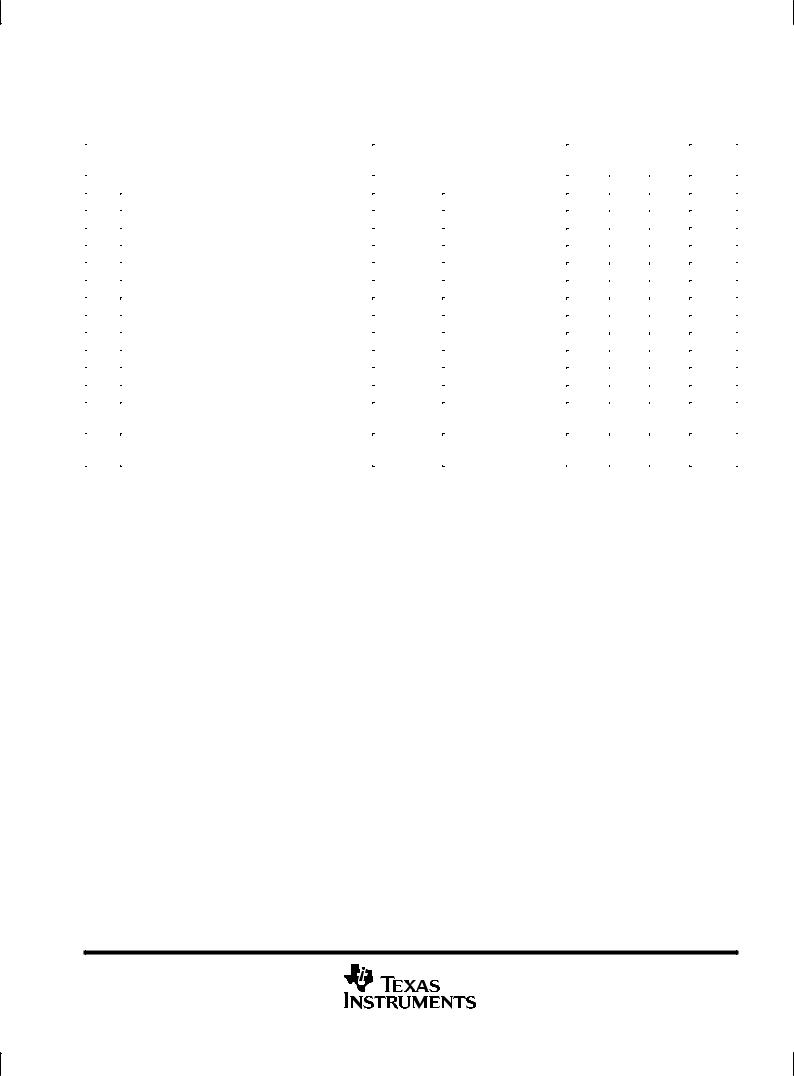
To overcome this limitation, TI design engineers developed the patented ESD-protection circuit shown in Figure 1. This circuit can withstand several successive 2-kV ESD pulses, while reducing or eliminating leakage currents that may be drawn through the input pins. A more detailed discussion of the operation of the TI ESD-protection circuit is presented on the next page.
All input and output pins on LinCMOS and Advanced LinCMOS products have associated ESD-protection circuitry that undergoes qualification testing to withstand 2000 V discharged from a 100-pF capacitor through a 1500-Ω resistor (human body model) and 200 V from a 100-pF capacitor with no current-limiting resistor (charged device model). These tests simulate both operator and machine handling of devices during normal test and assembly operations.
VDD
R1 |
|
Input |
|
|
R2 |
Q1 |
Q2 |
|
|
D1 |
D2 |
GND |
|
To Protected Circuit
D3
Figure 1. LinCMOS ESD-Protection Schematic
8 |
POST OFFICE BOX 655303 •DALLAS, TEXAS 75265 |
 Loading...