


Texas Instruments TL750L05QP, TL750L05QLP, TL750L05QKC, TL750L05CLPM, TL750L05CLP Datasheet
...
TL750L, TL751L SERIES LOW-DROPOUT VOLTAGE REGULATORS
SLVS017I ± SEPTEMBER 1987 ± REVISED JULY 1999
DVery Low Dropout Voltage, Less Than 0.6 V at 150 mA
DVery Low Quiescent Current
DTTLand CMOS-Compatible Enable on TL751L Series
D60-V Load-Dump Protection
DReverse Transient Protection Down to ±50 V
DInternal Thermal-Overload Protection
DOvervoltage Protection
DInternal Overcurrent-Limiting Circuitry
DLess Than 500- A Disable (TL751L Series)
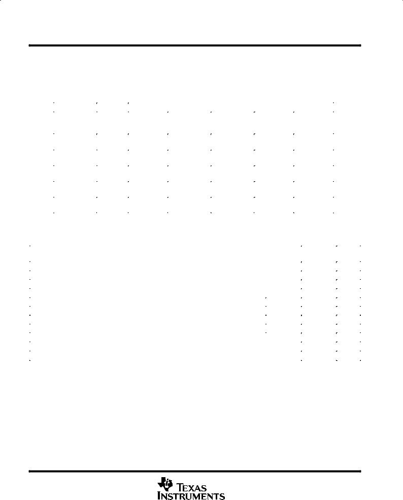
TL750L . . . D PACKAGE
(TOP VIEW)
OUTPUT |
|
|
1 |
8 |
|
INPUT |
|
|
|||||
COMMON |
|
|
2 |
7 |
|
COMMON |
COMMON |
|
|
3 |
6 |
|
COMMON |
NC |
|
|
4 |
5 |
|
NC |
|
|
|
|
|
|
|
TL750L . . . P PACKAGE
(TOP VIEW)
OUTPUT |
|
|
1 |
8 |
|
INPUT |
|
|
|||||
NC |
|
|
2 |
7 |
|
NC |
NC |
|
|
3 |
6 |
|
COMMON |
NC |
|
|
4 |
5 |
|
NC |
|
|
|
|
|
|
|
NC ± No internal connection
description
TL750L . . . KC PACKAGE
(TOP VIEW)
OUTPUT
COMMON
INPUT
The common terminal is in electrical contact with the mounting base.
TO-220AB
TL751L . . . D PACKAGE
(TOP VIEW)
TL750L . . . LP PACKAGE
(TOP VIEW)
INPUT
COMMON
OUTPUT
TO-226AA
TL751L . . . P PACKAGE
(TOP VIEW)
OUTPUT |
|
|
1 |
8 |
|
INPUT |
OUTPUT |
|
|
1 |
8 |
|
|
INPUT |
|||
|
|
|
|
|
|||||||||||||
COMMON |
|
|
2 |
7 |
|
COMMON |
NC |
|
|
2 |
7 |
|
|
NC |
|||
|
|
|
|
|
|
||||||||||||
COMMON |
|
|
3 |
6 |
|
COMMON |
NC |
|
|
3 |
6 |
|
|
COMMON |
|||
|
|
|
|
|
|
||||||||||||
NC |
|
|
4 |
5 |
|
|
ENABLE |
|
NC |
|
|
4 |
5 |
|
|
ENABLE |
|
|
|
|
|
|
|
||||||||||||
|
|
|
|
|
|
|
|
|
|
|
|
|
|
|
|
|
|
DEVICE
COMPONENT
COUNT
Transistors 20
JFETs 2
Diodes 5
Resistors 16
The TL750L and TL751L series are low-dropout positive-voltage regulators specifically designed for battery-powered systems. These devices incorporate overvoltage and current-limiting protection circuitry, along with internal reverse-battery protection circuitry to protect the devices and the regulated system. The series is fully protected against 60-V load-dump and reverse-battery conditions. Extremely low quiescent current during full-load conditions makes these devices ideal for standby power systems.
The TL750L and TL751L series of fixed-output voltage regulators offers 5-V, 8-V, 10-V, and 12-V options. The TL751L series has the addition of an enable (ENABLE) input. When ENABLE is high, the regulator output is placed in the high-impedance state. This gives the designer complete control over power up, power down, or emergency shutdown.
Please be aware that an important notice concerning availability, standard warranty, and use in critical applications of Texas Instruments semiconductor products and disclaimers thereto appears at the end of this data sheet.
PRODUCTION DATA information is current as of publication date. Products conform to specifications per the terms of Texas Instruments standard warranty. Production processing does not necessarily include testing of all parameters.
Copyright 1999, Texas Instruments Incorporated
POST OFFICE BOX 655303 •DALLAS, TEXAS 75265 |
1 |
TL750L, TL751L SERIES
LOW-DROPOUT VOLTAGE REGULATORS
SLVS017I ± SEPTEMBER 1987 ± REVISED JULY 1999
description (continued)
The TL750LxxC and the TL751LxxC series are characterized for operation over the virtual junction temperature range of 0°C to 125°C . The TL750L05Q and TL751L05Q are characterized for operation over the virtual junction temperature range of ±40°C to 125°C.
AVAILABLE OPTIONS
|
VO TYP |
|
PACKAGED DEVICES |
|
|
||
|
|
|
|
|
|
|
|
|
SMALL |
HEAT-SINK |
PLASTIC |
|
PLASTIC |
CHIP |
|
TJ |
AT |
|
|||||
OUTLINE |
MOUNTED |
CYLINDRICAL |
|
DIP |
FORM |
||
|
25°C |
|
|||||
|
(D) |
(KC) |
(LP) |
|
(P) |
(Y) |
|
|
|
|
|||||
|
|
|
|
|
|
|
|
|
5 V |
TL750L05CD |
TL750L05CKC |
TL750L05CLP |
|
TL750L05CP |
TL750L05Y |
|
TL751L05CD |
|
TL751L05CP |
||||
|
|
|
|
|
|
||
|
|
|
|
|
|
|
|
|
8 V |
TL750L08CD |
TL750L08CKC |
TL750L08CLP |
|
TL750L08CP |
TL750L08Y |
|
TL751L08CD |
|
TL751L08CP |
||||
0°C to 125°C |
|
|
|
|
|
||
|
|
|
|
|
|
|
|
10 V |
TL750L10CD |
TL750L10CKC |
TL750L10CLP |
|
TL750L10CP |
TL750L10Y |
|
|
|
||||||
|
TL751L10CD |
|
TL751L10CP |
||||
|
|
|
|
|
|
||
|
|
|
|
|
|
|
|
|
12 V |
TL750L12CD |
TL750L12CKC |
TL750L12CLP |
|
TL750L12CP |
TL750L12Y |
|
TL751L12CD |
|
TL751L12CP |
||||
|
|
|
|
|
|
||
|
|
|
|
|
|
|
|
±40°C to 125°C |
5 V |
TL750L05QD |
± |
± |
|
± |
± |
TL751L05QD |
|
||||||
|
|
|
|
|
|
|
|
|
|
|
|
|
|
|
|
The D, KTE, and LP packages are available taped and reeled. The KTP is only available taped and reeled. Add R suffix to device type (e.g., TL750L05CDR). Chip forms are tested at 25°C.
absolute maximum ratings over operating junction temperature range (unless otherwise noted)²
|
|
TL750Lxx |
UNIT |
|
|
|
TL751Lxx |
||
|
|
|
||
|
|
|
|
|
Continuous input voltage |
26 |
V |
||
|
|
|
|
|
Transient input voltage, TA = 25°C (see Note 1) |
60 |
V |
||
Continuous reverse input voltage |
±15 |
V |
||
|
|
|
|
|
Transient reverse input voltage: t ≤ 100 ms |
±50 |
V |
||
|
D package |
97 |
|
|
|
|
|
|
|
Package thermal impedance, θJA (see Notes 2 and 3) |
KC package |
22 |
°C |
|
|
|
|||
LP package |
156 |
|||
|
|
|||
|
|
|
|
|
|
P package |
127 |
|
|
|
|
|
|
|
Virtual junction temperature range, TJ |
±40 to 150 |
°C |
||
Lead temperature 1,6 mm (1/16 inch) for 10 seconds |
260 |
°C |
||
Storage temperature range, Tstg |
±65 to 150 |
°C |
||
²Stresses beyond those listed under ªabsolute maximum ratingsº may cause permanent damage to the device. These are stress ratings only, and functional operation of the device at these or any other conditions beyond those indicated under ªrecommended operating conditionsº is not
implied. Exposure to absolute-maximum-rated conditions for extended periods may affect device reliability. NOTES: 1. The transient input voltage rating applies to the waveform shown in Figure 1.
2.Maximum power dissipation is a function of TJ(max), θJA, and TA. The maximum allowable power dissipation at any allowable ambient temperature is PD = (TJ(max) ± TA)/θJA. Operating at the absolute maximum TJ of 150°C can impact reliability.
3.The package thermal impedance is calculated in accordance with JESD 51, except for through-hole packages, which use a trace length of zero.
2 |
POST OFFICE BOX 655303 •DALLAS, TEXAS 75265 |
TL750L, TL751L SERIES
LOW-DROPOUT VOLTAGE REGULATORS
SLVS017I ± SEPTEMBER 1987 ± REVISED JULY 1999
recommended operating conditions over recommended operating junction temperature range (unless otherwise noted)
|
|
|
|
|
MIN |
MAX |
UNITS |
|
|
|
|
|
|
|
|
|
|
|
|
TL75xL05 |
6 |
26 |
|
|
|
|
|
|
|
|
|
Input voltage, VI |
|
TL75xL08 |
9 |
26 |
V |
||
|
|
|
|
||||
|
TL75xL10 |
11 |
26 |
||||
|
|
|
|
|
|||
|
|
|
|
|
|
|
|
|
|
|
|
TL75xL12 |
13 |
26 |
|
|
|
|
|
|
|
||
High-level |
|
input voltage, VIH |
|
TL751Lxx |
2 |
15 |
V |
ENABLE |
|
||||||
Low-level ENABLE input voltage, VIL² |
TA = 25°C |
TL751Lxx |
±0.3 |
0.8 |
V |
||
T = full range³ |
TL751Lxx |
±0.15 |
0.8 |
||||
|
|
|
A |
|
|
|
|
Output current range, IO |
|
TL75xLxx |
0 |
150 |
mA |
||
Operating virtual junction temperature, TJ |
|
TL75xLxxC |
0 |
125 |
°C |
||
|
|
|
|
||||
|
TL75xL05Q |
±40 |
125 |
||||
|
|
|
|
|
|||
² The algebraic convention, in which the least positive (most negative) value is designated minimum, is used in this data sheet for ENABLE voltage levels and temperature only.
³ Full range is 0°C to 125°C for the TL75xLxxC devices, and ±40°C to 125°C for the TL75L05Q devices.
electrical characteristics, VI = 14 V, IO = 10 mA, TJ = 25°C (unless otherwise noted) (see Note 4)
|
|
|
|
|
|
|
|
|
|
|
|
|
TL750L05 |
|
|
PARAMETER |
|
|
|
|
|
|
TEST CONDITIONS§ |
|
|
|
|
TL751L05 |
|
UNIT |
|
|
|
|
|
|
|
|
|
|
|
|
|
MIN |
TYP |
MAX |
|
|
|
|
|
|
|
|
|
|
|
|
|
|
|
|
|
Output voltage |
|
|
|
|
|
|
|
|
|
|
|
4.80 |
5 |
5.2 |
V |
|
|
|
|
|
|
|
|
|
|
|
|
|
|
||
T |
= T |
J |
(min) to 125°C¶ |
|
|
|
|
|
4.75 |
|
5.25 |
||||
|
|
|
|
|
|
|
|
||||||||
|
|
J |
|
|
|
|
|
|
|
|
|
|
|
|
|
Input regulation voltage |
VI = 9 V to 16 V |
|
|
|
|
|
|
5 |
10 |
mV |
|||||
VI = 6 V to 26 V |
|
|
|
|
|
|
6 |
30 |
|||||||
|
|
|
|
|
|
|
|
||||||||
Ripple rejection |
VI = 8 V to 18 V, |
f = 120 Hz |
|
|
|
|
60 |
65 |
|
dB |
|||||
Output regulation voltage |
IO = 5 mA to 150 mA |
|
|
|
|
|
|
20 |
50 |
mV |
|||||
Dropout voltage |
IO = 10 mA |
|
|
|
|
|
|
|
0.2 |
V |
|||||
IO = 150 mA |
|
|
|
|
|
|
|
0.6 |
|||||||
|
|
|
|
|
|
|
|
|
|||||||
Output noise voltage |
f = 10 Hz to 100 kHz |
|
|
|
|
|
|
500 |
|
µV |
|||||
|
|
|
|
|
|
|
|
|
|
|
|
|
|||
|
IO = 150 mA |
|
|
|
|
|
|
10 |
12 |
|
|||||
Input bias current |
V = 6 V to 26 V, |
I = 10 mA, |
T |
= T |
J |
(min) to 125°C¶ |
|
1 |
2 |
mA |
|||||
|
|
I |
|
|
|
|
O |
J |
|
|
|
|
|
|
|
|
|
|
|
|
|
> 2 V |
|
|
|
|
|
|
|
0.5 |
|
|
|
ENABLE |
|
|
|
|
|
|
|
|
|||||
§Pulse-testing techniques are used to maintain the junction temperature as close to the ambient temperature as possible. Thermal effects must be taken into account separately. All characteristics are measured with a 0.1-µF capacitor across the input and a 10-µF capacitor, with equivalent series resistance of less than 0.4 Ω, across the output.
¶ TJ(min) is 0°C for the TL75xLxxC devices, and ±40°C for the TL75xLxxQ devices.
NOTE 4: For TL750L05Q/TL751L05Q, all characteristics are measured with a 0.1-µF tantalum capacitor on the output with equivalent series resistance within the guidelines shown in Figure 4.
POST OFFICE BOX 655303 •DALLAS, TEXAS 75265 |
3 |
 Loading...