


Texas Instruments TL062MJGB, TL064CPWR, TL064CPWLE, TL064CNSR, TL064CN Datasheet
...TL061, TL061A, TL061B, TL061Y, TL062, TL062A TL062B, TL062Y, TL064, TL064A, TL064B, TL064Y LOW-POWER JFET-INPUT OPERATIONAL AMPLIFIERS
SLOS078F ± NOVEMBER 1978 ± REVISED JANUARY 1999
DVery Low Power Consumption
DTypical Supply Current . . . 200 μA
(Per Amplifier)
DWide Common-Mode and Differential Voltage Ranges
DLow Input Bias and Offset Currents
DCommon-Mode Input Voltage Range Includes VCC+
DOutput Short-Circuit Protection
DHigh Input Impedance . . . JFET-Input Stage
DInternal Frequency Compensation
DLatch-Up-Free Operation
DHigh Slew Rate . . . 3.5 V/μs Typ
description
The JFET-input operational amplifiers of the TL06_ series are designed as low-power versions of the TL08_ series amplifiers. They feature high input impedance, wide bandwidth, high slew rate, and low input offset and input bias currents. The TL06_ series feature the same terminal assignments as the TL07_ and TL08_ series. Each of these JFET-input operational amplifiers incorporates well-matched, high-voltage JFET and bipolar transistors in a monolithic integrated circuit.
The C-suffix devices are characterized for operation from 0°C to 70°C. The I-suffix devices are characterized for operation from ±40°C to 85°C, and the M-suffix devices are characterized for operation over the full military temperature range of ±55°C to 125°C.
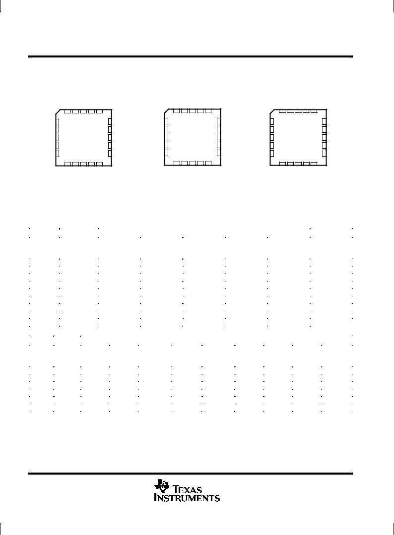
TL061, TL061A, TL061B D, JG, P, OR PW PACKAGE (TOP VIEW)
OFFSET N1 |
1 |
8 |
NC |
|
IN± |
2 |
7 |
VCC+ |
|
IN+ |
3 |
6 |
OUT |
|
VCC± |
4 |
5 |
OFFSET N2 |
|
TL061 . . . U PACKAGE |
||||
|
(TOP VIEW) |
|
||
|
|
|
|
|
NC |
|
•1 |
10 |
NC |
OFFSET N1 |
|
2 |
9 |
NC |
IN± |
|
3 |
8 |
VCC+ |
IN+ |
|
4 |
7 |
OUT |
VCC± |
|
5 |
6 |
OFFSET N2 |
TL062, TL062A, TL062B D, JG, P, OR PW PACKAGE (TOP VIEW)
1OUT |
1 |
8 |
|
VCC+ |
|
1IN± |
2 |
7 |
|
2OUT |
|
1IN+ |
3 |
6 |
|
2IN± |
|
VCC± |
4 |
5 |
|
2IN+ |
|
TL062 . . . U PACKAGE |
|||||
|
|
(TOP VIEW) |
|
||
|
|
|
|
|
|
NC |
|
•1 |
10 |
|
NC |
|
|
||||
1OUT |
|
2 |
9 |
|
VCC+ |
|
|
||||
1IN± |
|
3 |
8 |
|
2OUT |
|
|
||||
1IN+ |
|
4 |
7 |
|
2IN± |
|
|
||||
VCC± |
|
5 |
6 |
|
2IN+ |
|
|
||||
|
|
|
|
|
|
TL064 . . . D, J, N, PW, OR W PACKAGE TL064A, TL064B . . . D OR N PACKAGE (TOP VIEW)
1OUT |
|
1 |
14 |
|
4OUT |
|
|
||||
1IN± |
|
2 |
13 |
|
4IN± |
|
|
||||
1IN+ |
|
3 |
12 |
|
4IN+ |
|
|
||||
VCC+ |
|
4 |
11 |
|
VCC± |
|
|
||||
2IN+ |
5 |
10 |
|
3IN+ |
|
2IN± |
6 |
9 |
|
3IN± |
|
2OUT |
7 |
8 |
|
3OUT |
|
|
|
|
|
|
|
NC ± No internal connection
Please be aware that an important notice concerning availability, standard warranty, and use in critical applications of Texas Instruments semiconductor products and disclaimers thereto appears at the end of this data sheet.
PRODUCTION DATA information is current as of publication date. Products conform to specifications per the terms of Texas Instruments standard warranty. Production processing does not necessarily include testing of all parameters.
Copyright 1999, Texas Instruments Incorporated
POST OFFICE BOX 655303 •DALLAS, TEXAS 75265 |
1 |
TL061, TL061A, TL061B, TL061Y, TL062, TL062A TL062B, TL062Y, TL064, TL064A, TL064B, TL064Y LOW-POWER JFET-INPUT OPERATIONAL AMPLIFIERS
SLOS078F ± NOVEMBER 1978 ± REVISED JANUARY 1999
TL061 . . . FK PACKAGE
(TOP VIEW)
|
NC |
OFFSET N1 |
NC |
NC |
NC |
|
NC |
3 |
2 |
1 |
20 19 |
NC |
|
4 |
|
|
|
18 |
||
IN± |
5 |
|
|
|
17 |
VCC+ |
NC |
6 |
|
|
|
16 |
NC |
IN+ |
7 |
|
|
|
15 |
OUT |
NC |
8 |
|
|
|
14 |
NC |
|
9 |
10 11 12 13 |
|
|||
NC CC± |
NC N2 |
NC |
V |
OFFSET |
|
TL062 . . . FK PACKAGE |
TL064 . . . FK PACKAGE |
(TOP VIEW) |
(TOP VIEW) |
|
NC |
1OUT |
NC |
CC+ |
NC |
|
V |
||||
NC |
3 |
2 |
1 |
20 19 |
|
4 |
|
|
|
18 |
|
1IN± |
5 |
|
|
|
17 |
NC |
6 |
|
|
|
16 |
1IN+ |
7 |
|
|
|
15 |
NC |
8 |
|
|
|
14 |
|
9 |
10 11 12 13 |
|||
|
NC |
CC± |
NC |
2IN+ |
NC |
|
V |
||||
|
|
1IN± |
1OUT |
NC |
4OUT |
4IN± |
|
NC |
1IN+ |
3 |
2 |
1 |
20 19 |
4IN+ |
|
4 |
|
|
|
18 |
|||
2OUT |
NC |
5 |
|
|
|
17 |
NC |
NC |
VCC+ |
6 |
|
|
|
16 |
VCC± |
2IN± |
NC |
7 |
|
|
|
15 |
NC |
NC |
2IN+ |
8 |
|
|
|
14 |
3IN+ |
|
|
9 |
10 11 12 13 |
|
|||
|
|
2IN± |
2OUT |
NC |
3OUT |
3IN± |
|
NC ± No internal connection
AVAILABLE OPTIONS
|
|
|
|
|
|
|
|
|
|
PACKAGED DEVICES |
|
|
|
|
|
|
|
|
||||
|
|
VIOMAX |
|
|
|
|
|
|
|
|
|
|
|
|
|
|
|
|
CHIP FORM |
|||
TA |
|
|
|
SMALL |
SMALL |
|
PLASTIC |
|
|
PLASTIC |
|
TSSOP |
||||||||||
|
AT 25°C |
|
OUTLINE |
OUTLINE |
|
|
DIP |
|
|
DIP |
|
|
(Y) |
|||||||||
|
|
|
|
|
|
|
|
(PW) |
|
|
||||||||||||
|
|
|
|
|
|
(D008)² |
(D014)² |
|
|
(N) |
|
|
(P) |
|
|
|
|
|||||
|
|
|
|
|
|
|
|
|
|
|
|
|
|
|
|
|||||||
|
|
15 mV |
|
TL061CD |
|
|
|
|
|
|
|
|
TL061CP |
|
TL061CPW |
|
TL061Y |
|||||
|
|
6 mV |
|
TL061ACD |
|
|
|
|
|
|
|
TL061ACP |
|
|
|
|
|
|
||||
|
|
3 mV |
|
TL061BCD |
|
|
|
|
|
|
|
TL061BCP |
|
|
|
|
|
|
||||
0°C |
|
|
|
|
|
|
|
|
|
|
|
|
|
|
|
|
|
|
|
|
|
|
|
15 mV |
|
TL062CD |
|
|
|
|
|
|
|
|
TL062CP |
|
TL062CPW |
|
TL062Y |
||||||
to |
|
6 mV |
|
TL062ACD |
|
|
|
|
|
|
|
TL062ACP |
|
|
|
|
|
|
||||
70°C |
|
3 mV |
|
TL062BCD |
|
|
|
|
|
|
|
TL062BCP |
|
|
|
|
|
|
||||
|
|
|
|
|
|
|
|
|
|
|
|
|
|
|
|
|
|
|
|
|
||
|
|
15 mV |
|
|
|
|
TL064CD |
|
TL064CN |
|
|
|
|
TL064CPW |
|
TL064Y |
||||||
|
|
6 mV |
|
|
|
|
TL064ACD |
|
TL064ACN |
|
|
|
|
|
|
|
|
|
||||
|
|
3 mV |
|
|
|
|
TL064BCD |
|
TL064BCN |
|
|
|
|
|
|
|
|
|
||||
|
|
|
|
|
|
|
|
|
|
|
|
|
|
|
|
|
|
|
|
|
|
|
|
|
|
|
|
|
|
|
|
|
|
|
|
|
|
|
|
|
|
|
|
|
|
|
|
|
|
|
|
|
|
|
|
|
|
|
PACKAGE |
|
|
|
|
|
|
|
|
|
|
VIOMAX |
|
|
|
|
|
|
|
|
|
|
|
|
|
|
|
||||||
TA |
SMALL |
|
SMALL |
|
CHIP |
|
CERAMIC |
|
CERAMIC |
|
PLASTIC |
PLASTIC |
|
FLAT |
FLAT |
|||||||
AT 25°C |
OUTLINE |
|
OUTLINE |
|
CARRIER |
|
DIP |
|
DIP |
|
DIP |
|
DIP |
|
PACK |
PACK |
||||||
|
|
|
(D008)² |
|
(D014)² |
|
(FK) |
|
|
(J) |
|
(JG) |
|
(N) |
|
(P) |
|
(U) |
(W) |
|||
±40°C |
|
|
TL061ID |
|
|
|
|
|
|
|
|
|
|
|
|
|
TL061IP |
|
|
|
|
|
to |
|
6 mV |
|
TL064ID |
|
|
|
|
|
|
|
|
|
TL064IN |
|
|
|
|
|
|||
|
TL062ID |
|
|
|
|
|
|
|
|
|
|
|
TL062IP |
|
|
|
|
|||||
85°C |
|
|
|
|
|
|
|
|
|
|
|
|
|
|
|
|
|
|
|
|||
|
|
|
|
|
|
|
|
|
|
|
|
|
|
|
|
|
|
|
|
|
|
|
|
|
|
|
|
|
|
|
|
|
|
|
|
|
|
|
|
|
|
|
|
||
±55°C |
|
6 mV |
|
|
|
|
|
TL061MFK |
|
|
|
|
TL061MJG |
|
|
|
|
|
TL061MU |
|
||
to |
|
6 mV |
|
|
|
|
|
TL062MFK |
|
|
|
|
TL062MJG |
|
|
|
|
|
TL062MU |
|
||
125°C |
|
9 mV |
|
|
|
|
|
TL064MFK |
|
TL064MJ |
|
|
|
|
|
|
|
|
|
|
TL064MW |
|
|
|
|
|
|
|
|
|
|
|
|
|
|
|
|
|
|
|
|
|
|
|
|
² The D package is available taped and reeled. Add the suffix R to the device type (e.g., TL061CDR).
2 |
POST OFFICE BOX 655303 •DALLAS, TEXAS 75265 |
TL061, TL061A, TL061B, TL061Y, TL062, TL062A
TL062B, TL062Y, TL064, TL064A, TL064B, TL064Y
LOW-POWER JFET-INPUT OPERATIONAL AMPLIFIERS
SLOS078F ± NOVEMBER 1978 ± REVISED JANUARY 1999
symbol (each amplifier)
IN+ |
|
+ |
|
OUT |
|
|
|||
|
|
|
||
IN± |
|
± |
|
|
|
|
|||
|
|
|
||
|
|
|
|
|
|
OFFSET N1 OFFSET N2 |
|||
|
Offset Null/Compensation |
|||
|
TL061 Only |
|||
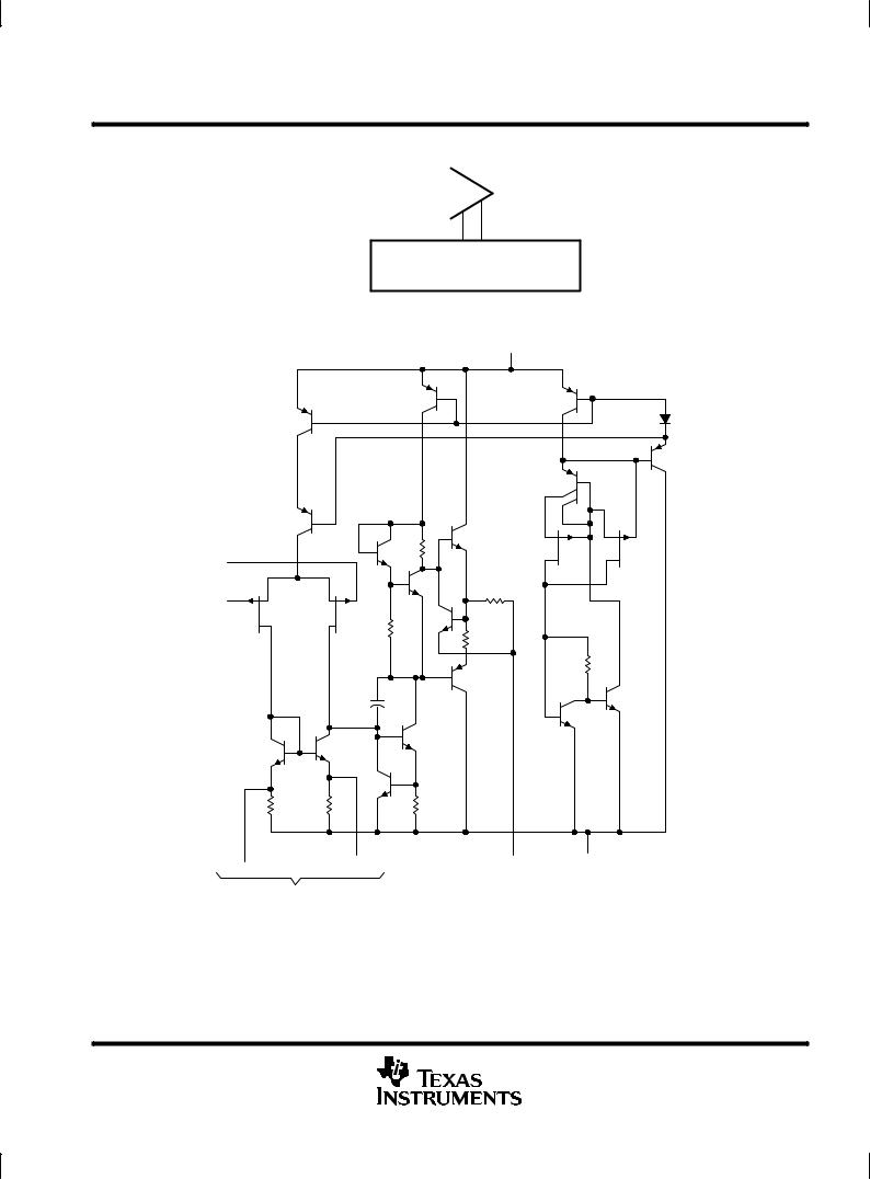
schematic (each amplifier) |
|
|
|
|
|
|
|
VCC+ |
|
IN+
50 Ω
IN±
100 Ω
C1
OFFSET N1 |
OFFSET N2 |
OUT |
VCC± |
TL061 Only
C1 = 10 pF on TL061, TL062, and TL064
Component values shown are nominal.
POST OFFICE BOX 655303 •DALLAS, TEXAS 75265 |
3 |

TL061, TL061A, TL061B, TL061Y, TL062, TL062A
TL062B, TL062Y, TL064, TL064A, TL064B, TL064Y
LOW-POWER JFET-INPUT OPERATIONAL AMPLIFIERS
SLOS078F ± NOVEMBER 1978 ± REVISED JANUARY 1999
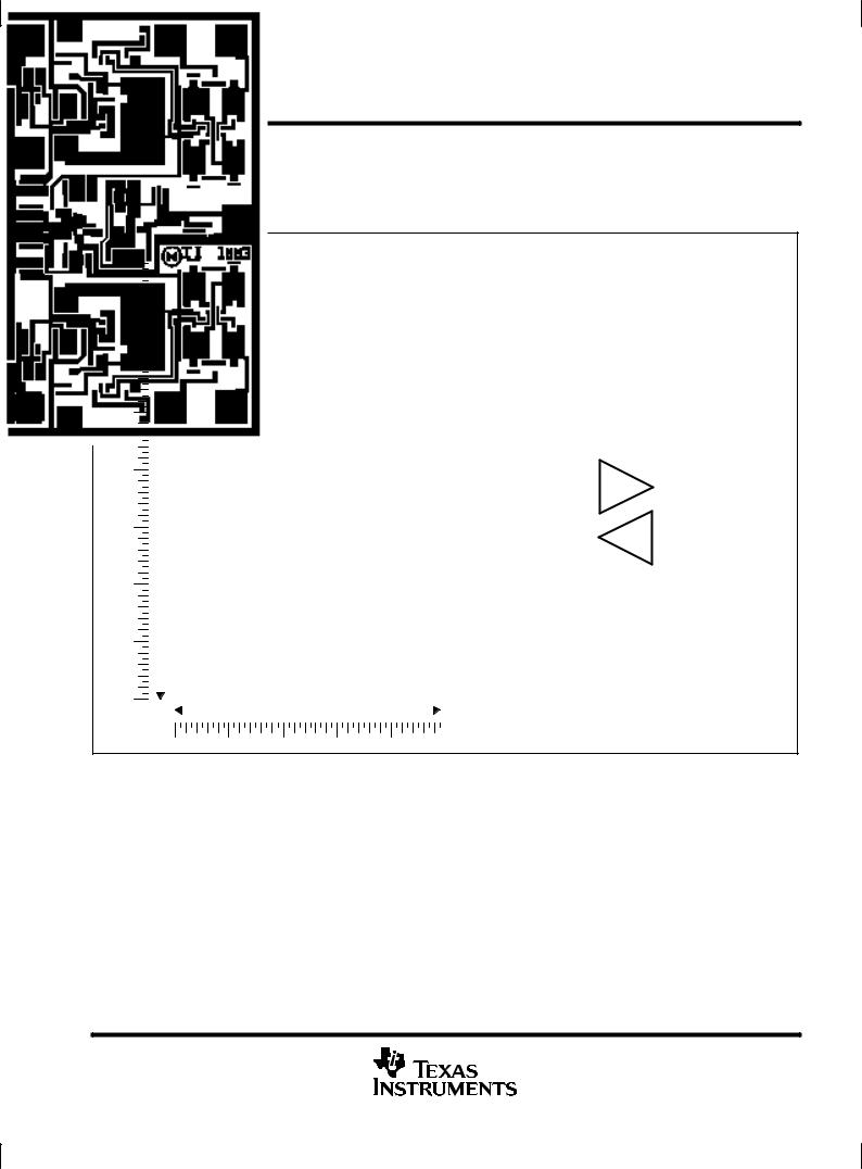
TL061Y chip information
This chip, when properly assembled, has characteristics similar to the TL061. Thermal compression or ultrasonic bonding can be used on the doped-aluminum bonding pads. The chips can be mounted with conductive epoxy or a gold-silicon preform.
Bonding-Pad Assignments
|
|
|
|
(5) |
(4) |
|
|
|
|
(6) |
|
|
(3) |
||
|
|
(7) |
|
|
|
||
41 |
|
|
|
|
|||
|
|
(8) |
(1) |
(2) |
|||
|
|
|
|
|
|
|
|
|
|
|
|
|
|
|
|
|
|
|
|
|
53 |
|
|
OFFSET N1 |
|
(1) |
|
VCC+ |
|
|
||
|
(3) |
|
|
|
(7) |
|
|
|
|
|
|
|
|
|
|||
IN+ |
+ |
|
|
(6) |
||||
|
|
|
|
|||||
|
|
|
|
|
|
|
||
IN± |
(2) |
± |
|
|
|
OUT |
||
|
|
|
||||||
|
|
|
|
|||||
|
|
|
(4) |
|
|
|||
|
(5) |
|
|
|||||
|
|
|
||||||
OFFSET N2 |
|
|
|
|
|
|||
|
|
|
|
|
||||
|
|
|
VCC± |
|
|
|||
|
|
|
|
|
|
|||
Chip Thickness: 15 Mils Typical Bonding Pads: 4 × 4 Mils Minimum TJ(max) = 150°C
Tolerances Are ±10%.
All Dimensions Are in Mils. Pin (4) is Internally Connected to Backside of Chip.
4 |
POST OFFICE BOX 655303 •DALLAS, TEXAS 75265 |
TL061, TL061A, TL061B, TL061Y, TL062, TL062A
TL062B, TL062Y, TL064, TL064A, TL064B, TL064Y
LOW-POWER JFET-INPUT OPERATIONAL AMPLIFIERS
SLOS078F ± NOVEMBER 1978 ± REVISED JANUARY 1999
TL062Y chip information
This chip, when properly assembled, has characteristics similar to the TL062. Thermal compression or ultrasonic bonding can be used on the doped-aluminum bonding pads. The chips can be mounted with conductive epoxy or a gold-silicon preform.
Bonding-Pad Assignments
|
|
|
|
(7) |
(6) |
(5) |
||
|
|
(8) |
|
|
|
|||
|
|
|
|
|
|
|
||
66 |
|
|
|
|
(4) |
|||
|
|
|
|
|
|
|
|
|
|
|
(1) |
(2) |
(3) |
||||
|
|
|
|
|
|
|
|
|
|
|
|
|
|
|
|
|
|
|
|
|
|
|
|
49 |
|
|
|
|
|
VCC+ |
|
|
|
|
|
(3) |
|
|
(8) |
|
|
|
1IN+ |
+ |
|
|
|
|
||
|
|
(1) |
|
1OUT |
|||
(2) |
|
||||||
1IN± |
± |
|
|
||||
|
|
|
|||||
|
|
||||||
|
|
|
|
||||
|
|
(5) |
|
|
|||
|
|
|
|||||
|
|
+ |
|
2IN+ |
|||
2OUT |
(7) |
|
|
||||
|
|
||||||
|
|
|
|
|
|||
|
|
|
± |
(6) |
|
2IN± |
|
|
|
|
|
||||
|
|
|
|
|
|||
|
|
|
|
|
|||
|
|
|
|
||||
|
|
|
(4) |
|
|
|
|
|
|
|
VCC± |
|
|
|
|
Chip Thickness: 15 Mils Typical Bonding Pads: 4 × 4 Mils Minimum TJ(max) = 150°C
Tolerances Are ±10%.
All Dimensions Are in Mils.
Pin (4) is Internally Connected to Backside of Chip.
POST OFFICE BOX 655303 •DALLAS, TEXAS 75265 |
5 |

TL061, TL061A, TL061B, TL061Y, TL062, TL062A
TL062B, TL062Y, TL064, TL064A, TL064B, TL064Y
LOW-POWER JFET-INPUT OPERATIONAL AMPLIFIERS
SLOS078F ± NOVEMBER 1978 ± REVISED JANUARY 1999
TL064Y chip information
This chip, when properly assembled, has characteristics similar to the TL064. Thermal compression or ultrasonic bonding can be used on the doped-aluminum bonding pads. The chips can be mounted with conductive epoxy or a gold-silicon preform.
Bonding-Pad Assignments
|
|
|
|
(13) |
(12) |
(11) |
(10) |
(9) |
|
|
(14) |
|
|
|
(8) |
||
|
|
|
|
|
|
|
||
60 |
|
|
|
|
|
|||
|
|
(1) |
|
|
|
(7) |
||
|
|
(2) |
(3) |
(4) |
(5) |
(6) |
||
|
|
|
|
|
|
|
|
|
|
|
|
|
|
|
|
|
|
|
|
|
|
|
|
110 |
|
|
|
|
VCC+ |
|
|
|
||
|
(3) |
|
|
(4) |
|
|
|
1IN+ |
+ |
|
|
|
|
|
|
|
|
(1) |
|
1OUT |
|||
|
|
|
|
|
|
||
1IN± |
(2) |
± |
|
|
|
|
|
|
|
|
|
|
|||
|
|
|
(5) |
|
|
||
|
|
+ |
|
2IN+ |
|||
2OUT |
(7) |
|
|
||||
|
|
||||||
|
|
|
|
|
|||
|
± |
(6) |
|
2IN± |
|||
|
|
||||||
|
|
|
|||||
4IN+ |
(10) |
|
|
||||
|
|
||||||
+ |
|
|
|
|
|
||
|
|
|
(8) |
|
4OUT |
||
|
|
|
|
|
|
||
4IN± |
(9) |
± |
|
|
|
|
|
|
|
|
|
|
|||
|
|
|
(12) |
|
|||
|
|
|
|
||||
|
|
+ |
3IN+ |
||||
3OUT |
(14) |
|
|
||||
|
|
||||||
|
|
|
|
|
|
||
|
|
± |
(13) |
|
3IN± |
||
|
|
|
|||||
|
|
|
|
||||
|
|
|
|
|
|||
|
|
|
(11) |
|
|
|
|
VCC±
Chip Thickness: 15 Mils Typical Bonding Pads: 4 × 4 Mils Minimum TJ(max) = 150°C
Tolerances Are ±10%.
All Dimensions Are in Mils.
Pin (11) is Internally Connected to Backside of Chip.
6 |
POST OFFICE BOX 655303 •DALLAS, TEXAS 75265 |

TL061, TL061A, TL061B, TL061Y, TL062, TL062A
TL062B, TL062Y, TL064, TL064A, TL064B, TL064Y
LOW-POWER JFET-INPUT OPERATIONAL AMPLIFIERS
SLOS078F ± NOVEMBER 1978 ± REVISED JANUARY 1999
absolute maximum ratings over operating free-air temperature range (unless otherwise noted)²
|
|
TL06_C |
|
|
|
|
|
|
TL06_AC |
TL06_I |
|
TL06_M |
UNIT |
|
|
TL06_BC |
|
|
|
|
|
|
|
|
|
|
|
Supply voltage, VCC+ (see Note 1) |
|
18 |
18 |
|
18 |
V |
Supply voltage, VCC± (see Note 1) |
|
±18 |
±18 |
|
±18 |
V |
Differential input voltage, VID (see Note 2) |
|
±30 |
±30 |
|
±30 |
V |
Input voltage, VI (see Notes 1 and 3) |
|
±15 |
±15 |
|
±15 |
V |
Duration of output short circuit (see Note 4) |
|
unlimited |
unlimited |
|
unlimited |
|
|
|
|
|
|
|
|
Continuous total dissipation |
|
See Dissipation Rating Table |
|
|
||
|
|
|
|
|
|
|
Storage temperature range, Tstg |
|
±65 to 150 |
±65 to 150 |
|
±65 to 150 |
°C |
Case temperature for 60 seconds |
FK package |
|
|
|
260 |
°C |
|
|
|
|
|
|
|
Lead temperature 1,6 mm (1/16 inch) from case for 60 seconds |
J, JG, U, or |
|
|
|
300 |
°C |
W package |
|
|
|
|||
|
|
|
|
|
|
|
|
|
|
|
|
|
|
Lead temperature 1,6 mm (1/6 inch) from case for 10 seconds |
D, N, P, or |
260 |
260 |
|
|
°C |
PW package |
|
|
||||
|
|
|
|
|
|
|
|
|
|
|
|
|
|
²Stresses beyond those listed under ªabsolute maximum ratingsº may cause permanent damage to the device. These are stress ratings only, and functional operation of the device at these or any other conditions beyond those indicated under ªrecommended operating conditionsº is not implied. Exposure to absolute-maximum-rated conditions for extended periods may affect device reliability.
NOTES: 1. All voltage values except differential voltages are with respect to the midpoint between VCC+ and VCC±.
2.Differential voltages are at IN+ with respect to IN±.
3.The magnitude of the input voltage must never exceed the magnitude of the supply voltage or 15 V, whichever is less.
4.The output may be shorted to ground or to either supply. Temperature and/or supply voltages must be limited to ensure that the dissipation rating is not exceeded.
DISSIPATION RATING TABLE
PACKAGE |
TA ≤ 25°C |
DERATING |
DERATE |
TA = 70°C |
TA = 85°C |
TA = 125°C |
|
POWER RATING |
FACTOR |
ABOVE TA |
POWER RATING |
POWER RATING |
POWER RATING |
||
|
|||||||
D (8 pin) |
680 mW |
5.8 mW/°C |
33°C |
465 mW |
378 mW |
N/A |
|
D (14 pin) |
680 mW |
7.6 mW/°C |
60°C |
604 mW |
490 mW |
N/A |
|
FK |
680 mW |
11.0 mW/°C |
88°C |
680 mW |
680 mW |
273 mW |
|
J |
680 mW |
11.0 mW/°C |
88°C |
680 mW |
680 mW |
273 mW |
|
JG |
680 mW |
8.4 mW/°C |
69°C |
672 mW |
546 mW |
210 mW |
|
N |
680 mW |
9.2 mW/°C |
76°C |
680 mW |
597 mW |
N/A |
|
P |
680 mW |
8.0 mW/°C |
65°C |
640 mW |
520 mW |
N/A |
|
PW (8 pin) |
525 mW |
4.2 mW/°C |
25°C |
336 mW |
N/A |
N/A |
|
PW (14 pin) |
700 mW |
5.6 mW/°C |
25°C |
448 mW |
N/A |
N/A |
|
U |
675 mW |
5.4 mW/°C |
25°C |
432 mW |
351 mW |
135 mW |
|
W |
680 mW |
8.0 mW/°C |
65°C |
640 mW |
520 mW |
200 mW |
|
|
|
|
|
|
|
|
POST OFFICE BOX 655303 •DALLAS, TEXAS 75265 |
7 |
 Loading...