


MC10E157FNR2
NC V
CCO
Q
3
V
CCO
D
3
bD
3
aNCSEL3
LOGIC DIAGRAM
D
2
b
D
2
a
SEL2
V
EE
SEL1
D
1
a
D
1
b
26
27
28
2
3
4
25 24 23 22 21 20 19
18
17
16
15
14
13
12
115 6 7 8 9 10
Q
3
Q
2
Q
2
V
CC
Q
1
Q
1
Q
0
Q
0
SEL0 D
0
a D
0
b NC NC
D
0
a
D
0
b
SEL0
D
1
a
D
1
b
SEL1
D
2
a
D
2
b
SEL2
D
3
a
D
3
b
SEL3
Q
0
Q
0
Q
1
Q
1
Q
2
Q
2
Q
3
Q
3
MUX
MUX
MUX
MUX
1
0
1
0
1
0
1
0
1
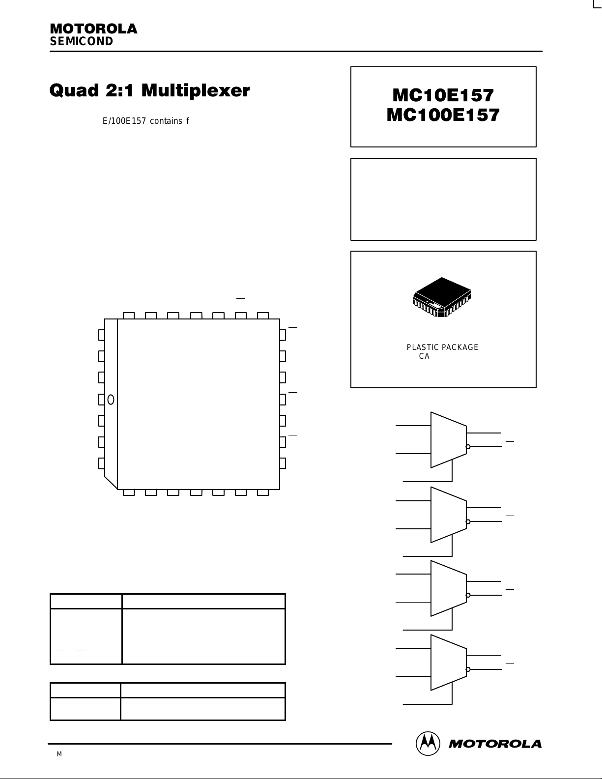
Pinout: 28-Lead PLCC (Top View)
* All V
CC
and V
CCO
pins are tied together on the die.
SEMICONDUCTOR TECHNICAL DATA
2–1
REV 2
Motorola, Inc. 1996
12/93
The MC10E/100E157 contains four 2:1 multiplexers with differential
outputs. The output data are controlled by the individual Select (SEL)
inputs. The individual select control makes the devices well suited for
random logic designs.
• Individual Select Controls
• 550ps Max. D to Output
• 800ps Max. SEL to Output
• Extended 100E V
EE
Range of – 4.2V to – 5.46V
• Internal 75kΩ Input Pulldown Resistors
PIN NAMES
Pin Function
D
0
a – D
3
a Input Data a
D
0
b – D
3
b Input Data b
SEL0 – SEL3 Select Inputs
Q
0
– Q
3
True Outputs
Q
0
– Q
3
Inverted Outputs
TRUTH TABLE
SEL Data
H
L
a
b
QUAD 2:1
MULTIPLEXER
FN SUFFIX
PLASTIC PACKAGE
CASE 776-02
MC10E157 MC100E157
MOTOROLA ECLinPS and ECLinPS Lite
DL140 — Rev 4
2–2
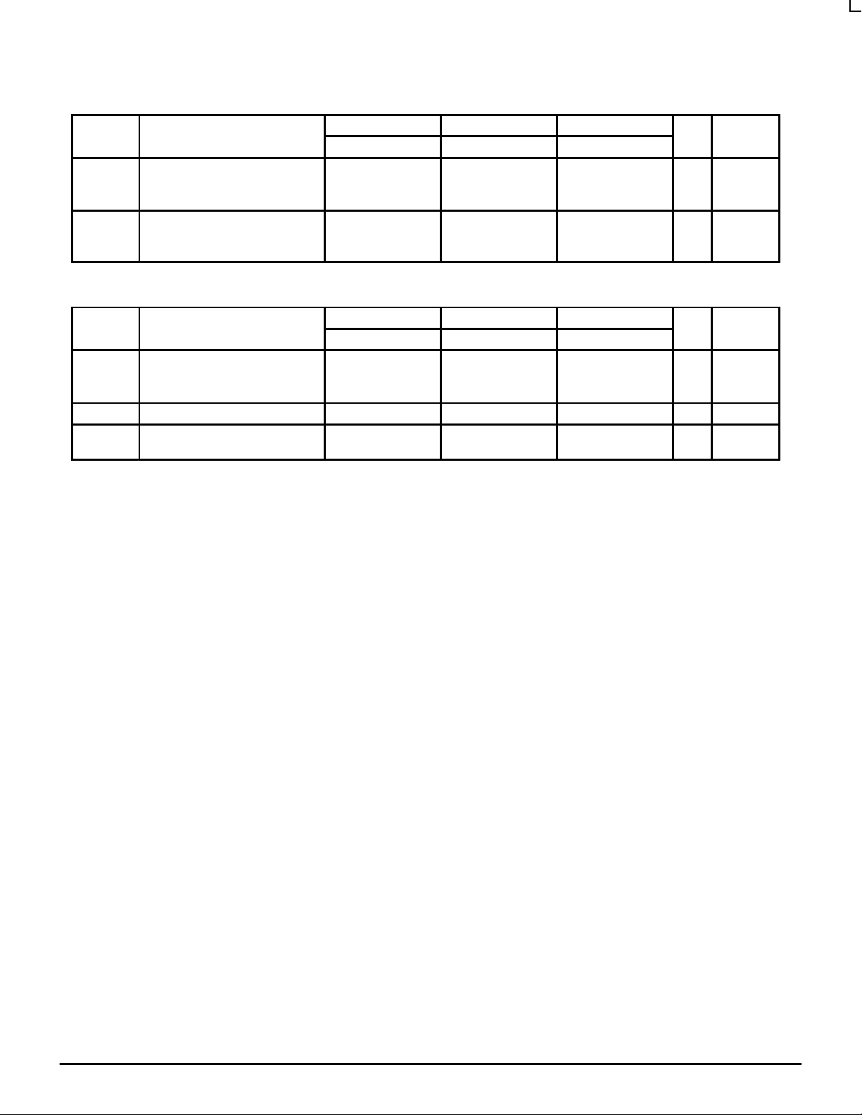
DC CHARACTERISTICS (V
EE
= V
EE
(min) to V
EE
(max); V
CC
= V
CCO
= GND)
0°C 25°C 85°C
Symbol Characteristic min typ max min typ max min typ max Unit Condition
I
IH
Input HIGH Current µA
D 200 200 200
SEL 150 150 150
I
EE
Power Supply Current mA
10E 32 38 32 38 32 38
100E 32 38 32 38 37 44
AC CHARACTERISTICS (V
EE
= V
EE
(min) to V
EE
(max); V
CC
= V
CCO
= GND)
0°C 25°C 85°C
Symbol Characteristic min typ max min typ max min typ max Unit Condition
t
PLH
Propagation Delay to Output ps
t
PHL
D 220 380 550 220 380 550 220 380 550
SEL 425 600 800 425 600 800 425 600 800
t
SKEW
Within-Device Skew 70 70 70 ps 1
t
r
Rise/Fall Times ps
t
f
20 - 80% 275 400 650 275 400 650 275 400 650
1. Within-device skew is defined as identical transitions on similar paths through a device.
 Loading...