


MOTOROLA
SEMICONDUCTOR TECHNICAL DATA
Programmable Delay Chip
The MC10E/100E196 is a programmable delay chip (PDC) designed primarily for very accurate differential ECL input edge placement applications.
The delay section consists of a chain of gates and a linear ramp delay adjust organized as shown in the logic symbol. The first two delay elements feature gates that have been modified to have delays 1.25 and 1.5 times the basic gate delay of approximately 80 ps. These two elements provide the E196 with a digitally-selectable resolution of approximately 20 ps. The required device delay is selected by the seven address inputs D[0:6], which are latched on chip by a high signal on the latch enable (LEN) control.
The FTUNE input takes an analog voltage and applies it to an internal linear ramp for reducing the 20 ps resolution still further. The FTUNE input is what differentiates the E196 from the E195.
An eighth latched input, D7, is provided for cascading multiple PDC's for increased programmable range. The cascade logic allows full control of multiple PDC's, at the expense of only a single added line to the data bus for each additional PDC, without the need for any external gating.
•2.0ns Worst Case Delay Range
•≈20ps/Delay Step Resolution
•Linear Input for Tighter Resolution
•>1.0GHz Bandwidth
•On Chip Cascade Circuitry
•Extended 100E VEE Range of ±4.2 to ±5.46V
•75KΩ Input Pulldown Resistors
PIN NAMES
Pin |
Function |
|
|
IN/IN |
Signal Input |
EN |
Input Enable |
D[0:7] |
Mux Select Inputs |
Q/Q |
Signal Output |
LEN |
Latch Enable |
SET MIN |
Min Delay Set |
SET MAX |
Max Delay Set |
CASCADE |
Cascade Signal |
FTUNE |
Linear Voltage Input |
|
|
MC10E196
MC100E196
PROGRAMMABLE
DELAY CHIP
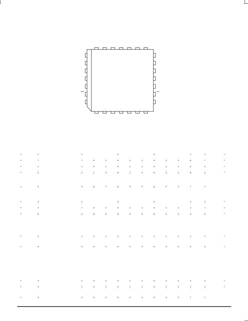
FN SUFFIX
PLASTIC PACKAGE
CASE 776-02
|
|
|
|
|
|
|
LOGIC DIAGRAM ± SIMPLIFIED |
|
|
|
||||
VBB |
|
|
|
|
|
|
|
|
|
|
|
FTUNE |
|
|
|
|
|
|
|
|
|
|
|
|
|
|
|
||
IN |
1 |
0 |
0 |
|
0 |
|
|
0 |
4 GATES |
0 |
0 |
0 |
|
|
|
|
|
|
|
|
|
|
|
8 GATES |
16 GATES |
|
|
||
IN |
|
1 |
1 |
1 |
1 |
1 |
1 |
1 |
|
1 |
1 |
1 |
|
|
|
|
|
0 |
Q |
||||||||||
EN |
|
|
|
|
|
|
|
|
|
|
|
|
||
* 1.25 |
|
* 1.5 |
|
|
|
|
|
|
|
|
|
|
Q |
|
|
|
|
|
|
|
|
|
|
|
1 |
1 |
|||
|
|
|
|
|
|
|
|
|
|
|
|
LINEAR |
||
|
|
|
|
|
|
|
|
|
|
|
|
|
|
|
|
|
|
|
|
|
|
|
|
|
|
|
CASCADE |
|
RAMP |
|
|
|
|
|
|
|
|
|
|
|
|
|
|
|
LEN |
|
|
|
|
|
|
|
|
|
|
LEN |
Q |
|
|
|
|
|
|
|
|
7 BIT LATCH |
|
|
|
|
|
|
||
SET MIN |
|
|
|
|
|
|
|
|
LATCH |
|
|
|||
SET MAX |
|
|
|
|
|
|
|
|
|
|
|
D |
|
CASCADE |
|
|
|
|
|
|
|
|
|
|
|
|
|
|
|
|
|
|
|
|
|
|
|
|
|
|
|
|
|
CASCADE |
|
|
|
D0 |
|
D1 |
D2 |
|
D3 |
D4 |
D5 |
D6 |
D7 |
|
|
* DELAYS ARE 25% OR 50% LONGER THAN |
|
|
|
|
|
|
|
|
|
|
|
|||
* STANDARD (STANDARD ≈ 80 PS) |
|
|
|
|
|
|
|
|
|
|
|
|||
12/93
Motorola, Inc. 1996 |
REV 2 |
MC10E196 MC100E196
Pinout: 28-Lead PLCC (Top View)
D2 |
D3 |
D4 |
25 |
24 |
23 |
D1 26
D0 27
LEN 28
VEE 1
IN 2
IN 3
VBB 4
5 |
6 |
7 |
|
|
|
|
|
NC |
NC |
EN |
|
D5 |
D6 |
D7 |
NC |
22 |
21 |
20 |
19 |
18 FTUNE
17 NC
16 VCC
15 VCCO
14 Q
13 Q
12 VCCO
8 |
9 |
10 |
11 |
|
SET MIN |
SET MAX |
CASCADE |
|
CASCADE |
|
||||
DC CHARACTERISTICS (VEE = VEE(min) to VEE(max); VCC = VCCO = GND)
|
|
|
0°C |
|
|
25°C |
|
|
85°C |
|
|
|
|
|
|
|
|
|
|
|
|
|
|
|
|
Symbol |
Characteristic |
Min |
Typ |
Max |
Min |
Typ |
Max |
Min |
Typ |
Max |
Unit |
Condition |
|
|
|
|
|
|
|
|
|
|
|
|
|
IIH |
Input HIGH Current |
|
|
150 |
|
|
150 |
|
|
150 |
μA |
|
IEE |
Power Supply Current |
|
130 |
156 |
|
130 |
156 |
|
130 |
156 |
mA |
|
|
10E |
|
|
|
|
|
||||||
|
100E |
|
130 |
156 |
|
130 |
156 |
|
150 |
179 |
|
|
|
|
|
|
|
|
|
|
|
|
|
|
|
AC CHARACTERISTICS (VEE = VEE(min) to VEE(max); VCC = VCCO = GND)
|
|
|
0°C |
|
|
25°C |
|
|
85°C |
|
|
|
|
|
|
|
|
|
|
|
|
|
|
|
|
Symbol |
Characteristic |
Min |
Typ |
Max |
Min |
Typ |
Max |
Min |
Typ |
Max |
Unit |
Notes |
|
|
|
|
|
|
|
|
|
|
|
|
|
tPLH |
Propagation Delay |
|
|
|
|
|
|
|
|
|
ps |
|
tPHL |
IN to Q; Tap = 0 |
1210 |
1360 |
1510 |
1240 |
1390 |
1540 |
1440 |
1590 |
1765 |
|
|
|
IN to Q; Tap = 127 |
3320 |
3570 |
3820 |
3380 |
3630 |
3880 |
3920 |
4270 |
4720 |
|
|
|
EN to Q; Tap = 0 |
1250 |
1450 |
1650 |
1275 |
1475 |
1675 |
1350 |
1650 |
1950 |
|
|
|
D7 to CASCADE |
300 |
450 |
700 |
300 |
450 |
700 |
300 |
450 |
700 |
|
|
|
|
|
|
|
|
|
|
|
|
|
|
|
tRANGE |
Programmable Range |
2000 |
2175 |
|
2050 |
2240 |
|
2375 |
2580 |
|
ps |
|
|
tPD (max) ± tPD (min) |
|
|
|
|
|
||||||
t |
Step Delay |
|
|
|
|
|
|
|
|
|
ps |
6 |
|
D0 High |
|
17 |
|
|
17.5 |
|
|
21 |
|
|
|
|
D1 High |
|
34 |
|
|
35 |
|
|
42 |
|
|
|
|
D2 High |
55 |
68 |
105 |
55 |
70 |
105 |
65 |
84 |
120 |
|
|
|
D3 High |
115 |
136 |
180 |
115 |
140 |
180 |
140 |
168 |
205 |
|
|
|
D4 High |
250 |
272 |
325 |
250 |
280 |
325 |
305 |
336 |
380 |
|
|
|
D5 High |
505 |
544 |
620 |
515 |
560 |
620 |
620 |
672 |
740 |
|
|
|
D6 High |
1000 |
1088 |
1190 |
1030 |
1120 |
1220 |
1240 |
1344 |
1450 |
|
|
|
|
|
|
|
|
|
|
|
|
|
|
|
Lin |
Linearity |
D1 |
D0 |
|
D1 |
D0 |
|
D1 |
D0 |
|
|
7 |
|
|
|
|
|
|
|
|
|
|
|
|
|
tSKEW |
Duty Cycle Skew |
|
±30 |
|
|
±30 |
|
|
±30 |
|
ps |
1 |
|
tPHL±tPLH |
|
|
|
|
|
|
|
MOTOROLA |
2±2 |

MC10E196 MC100E196
AC CHARACTERISTICS (continued) (VEE = VEE(min) to VEE(max); VCC = VCCO = GND)
|
|
|
0°C |
|
|
25°C |
|
|
85°C |
|
|
|
|
|
|
|
|
|
|
|
|
|
|
|
|
Symbol |
Characteristic |
Min |
Typ |
Max |
Min |
Typ |
Max |
Min |
Typ |
Max |
Unit |
Notes |
|
|
|
|
|
|
|
|
|
|
|
|
|
ts |
Setup Time |
200 |
0 |
|
200 |
0 |
|
200 |
0 |
|
ps |
|
|
D to LEN |
|
|
|
|
|
||||||
|
D to IN |
800 |
|
|
800 |
|
|
800 |
|
|
|
2 |
|
EN to IN |
200 |
|
|
200 |
|
|
200 |
|
|
|
3 |
|
|
|
|
|
|
|
|
|
|
|
|
|
th |
Hold Time |
500 |
250 |
|
500 |
250 |
|
500 |
250 |
|
ps |
|
|
LEN to D |
|
|
|
|
|
||||||
|
IN to EN |
0 |
|
|
0 |
|
|
0 |
|
|
|
4 |
|
|
|
|
|
|
|
|
|
|
|
|
|
tR |
Release Time |
|
|
|
|
|
|
|
|
|
ps |
|
|
EN to IN |
300 |
|
|
300 |
|
|
300 |
|
|
|
5 |
|
SET MAX to LEN |
800 |
|
|
800 |
|
|
800 |
|
|
|
|
|
SET MIN to LEN |
800 |
|
|
800 |
|
|
800 |
|
|
|
|
|
|
|
|
|
|
|
|
|
|
|
|
|
tjit |
Jitter |
|
<5.0 |
|
|
<5.0 |
|
|
<5.0 |
|
ps |
8 |
tr |
Output Rise/Fall Time |
|
|
|
|
|
|
|
|
|
ps |
|
tf |
20±80% (Q) |
125 |
225 |
325 |
125 |
225 |
325 |
125 |
225 |
325 |
|
|
|
20±80% (CASCADE) |
300 |
450 |
650 |
300 |
450 |
650 |
300 |
450 |
650 |
|
|
|
|
|
|
|
|
|
|
|
|
|
|
|
1.Duty cycle skew guaranteed only for differential operation measured from the cross point of the input to the cross point of the output.
2.This setup time defines the amount of time prior to the input signal the delay tap of the device must be set.
3.This setup time is the minimum time that EN must be asserted prior to the next transition of IN/IN to prevent an output response greater than
±75 mV to that IN/IN transition.
4.This hold time is the minimum time that EN must remain asserted after a negative going IN or positive going IN to prevent an output response greater than ±75 mV to that IN/IN transition.
5.This release time is the minimum time that EN must be deasserted prior to the next IN/IN transition to ensure an output response that meets the specified IN to Q propagation delay and transition times.
6.Specification limits represent the amount of delay added with the assertion of each individual delay control pin. The various combinations of asserted delay control inputs will typically realize D0 resolution steps across the specified programmable range.
7.The linearity specification guarantees to which delay control input the programmable steps will be monotonic (i.e. increasing delay steps for increasing binary counts on the control inputs Dn). Typically the device will be monotonic to the D0 input, however under worst case conditions and process variation, delays could decrease slightly with increasing binary counts when the D0 input is the LSB. With the D1 input as the LSB the device is guaranteed to be monotonic over all specified environmental conditions and process variation.
8.The jitter of the device is less than what can be measured without resorting to very tedious and specialized measurement techniques.
ANALOG INPUT CHARACTERISTICS
Ftune = VCC to VEE
|
140 |
|
|
|
|
|
120 |
|
|
|
|
(ps) |
100 |
|
|
|
(ps) |
DELAY |
|
|
|
DELAY |
|
80 |
|
|
|
||
PROPAGATION |
|
|
|
PROPAGATION |
|
60 |
|
|
|
||
40 |
|
|
|
||
|
|
|
|
||
|
20 |
|
|
|
|
|
0 |
|
|
|
|
|
±4.5 |
±3.5 |
±2.5 |
±1.5 |
±0.5 |
100 |
|
|
|
|
|
90 |
|
|
|
|
|
80 |
|
|
|
|
|
70 |
|
|
|
|
|
60 |
|
|
|
|
|
50 |
|
|
|
|
|
40 |
|
|
|
|
|
30 |
|
|
|
|
|
20 |
|
|
|
|
|
10 |
|
|
|
|
|
0 |
|
|
|
|
|
±5 |
±4 |
±3 |
±2 |
±1 |
0 |
FTUNE VOLTAGE (V) |
FTUNE VOLTAGE (V) |
Propagation Delay versus Ftune Voltage |
Propagation Delay versus Ftune Voltage |
(100E196) |
(10E196) |
2±3 |
MOTOROLA |
 Loading...