


MOTOROLA
SEMICONDUCTOR TECHNICAL DATA
3 Bit Scannable Registered
Address Driver
The MC10E/100E212 is a scannable registered ECL driver typically used as a fan-out memory address driver for ECL cache driving. In a VLSI array based CPU design, use of the E212 allows the user to conserve array output cell functionality and also output pins.
The input shift register is designed with control logic which greatly facilitates its use in boundary scan applications.
•Scannable Version E112 Driver
•1025ps Max. CLK to Output
•Dual Differential Outputs
•Master Reset
•Extended 100E VEE Range of ± 4.2V to ± 5.46V
•Internal 75kΩ Input Pulldown Resistors
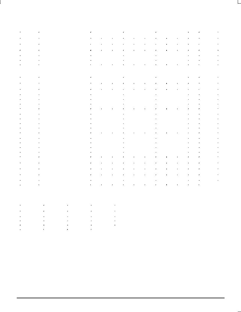
Pinout: 28-Lead PLCC (Top View)
|
|
|
|
|
|
|
SHIFT |
|
MR |
NC |
S-OUTVCCO Q2b |
Q2a |
|
|
|
|
||||||||||||||||||
|
|
|
|
|
|
|
|
|
|
|
|
|
|
|
|
|
|
|
|
|
|
|
|
|
|
|
|
|
|
|
|
|
|
|
|
|
|
|
|
|
|
25 |
|
24 |
|
23 |
|
22 |
|
21 |
|
|
20 |
|
|
19 |
|
|
|
|
|
|
|
||||||
|
|
|
|
|
|
|
|
|
|
|||||||||||||||||||||||||
|
|
LOAD |
|
|
26 |
|
|
|
|
|
|
|
|
|
|
|
|
|
|
|
|
|
|
|
18 |
|
|
Q2b |
|
|
||||
|
|
CLK |
|
27 |
|
|
|
|
|
|
|
|
|
|
|
|
|
|
|
|
|
|
|
17 |
|
|
Q2a |
|
|
|||||
|
|
|
|
|
|
|
|
|
|
|
|
|
|
|
|
|
|
|
|
|
|
|
|
|
|
|
||||||||
|
|
D2 |
|
|
28 |
|
|
|
|
|
|
|
|
|
|
|
|
|
|
|
|
|
|
|
16 |
|
|
|
|
|||||
|
|
|
|
|
|
|
|
|
|
|
|
|
|
|
|
|
|
|
|
|
|
|
|
VCC |
|
|
||||||||
|
|
|
|
|
|
|
|
|
|
|
|
|
|
|
|
|
|
|
|
|
|
|
|
|
|
|
||||||||
|
|
|
|
|
|
|
|
|
|
|
|
|
|
|
|
|
|
|
|
|
|
|
15 |
|
|
|
|
|||||||
|
|
VEE |
|
1 |
|
|
|
|
|
|
|
|
|
|
|
|
|
|
|
|
|
|
|
|
|
Q1b |
|
|
|
|||||
|
|
|
|
|
|
|
|
|
|
|
|
|
|
|
|
|
|
|
|
|
|
|
|
|
|
|
||||||||
|
|
D1 |
|
|
2 |
|
|
|
|
|
|
|
|
|
|
|
|
|
|
|
|
|
|
|
14 |
|
|
|
|
|
|
|||
|
|
|
|
|
|
|
|
|
|
|
|
|
|
|
|
|
|
|
|
|
|
|
|
|
Q1a |
|
|
|||||||
|
|
|
|
|
|
|
|
|
|
|
|
|
|
|
|
|
|
|
|
|
|
|
|
|
|
|
||||||||
|
|
|
|
|
|
|
|
|
|
|
|
|
|
|
|
|
|
|
|
|
|
|
|
|
|
|
|
|
|
|||||
|
|
D0 |
|
|
3 |
|
|
|
|
|
|
|
|
|
|
|
|
|
|
|
|
|
|
|
13 |
|
|
Q1b |
|
D2 |
||||
|
|
|
|
|
|
|
|
|
|
|
|
|
|
|
|
|
|
|
|
|
|
|
|
|
|
|||||||||
|
|
|
|
|
|
|
|
|
|
|
|
|
|
|
|
|
|
|
|
|
|
|
|
|
|
|
|
|
||||||
|
|
S-IN |
|
|
4 |
|
|
|
|
|
|
|
|
|
|
|
|
|
|
|
|
|
|
|
12 |
|
|
Q1a |
|
|
||||
|
|
|
|
|
|
|
|
|
|
|
|
|
|
|
|
|
|
|
|
|
|
|
|
|
|
|
||||||||
|
|
|
|
|
|
|
5 |
|
6 |
|
7 |
|
8 |
|
9 |
|
|
10 |
|
|
11 |
|
|
|
|
|
|
|
||||||
|
|
|
|
|
|
|
|
|
|
|
|
|
|
|
|
|
|
|
|
|
||||||||||||||
|
|
|
|
|
|
|
|
|
|
|
|
|
|
|
|
|
|
|
|
|
|
|
|
|
|
|
|
|
|
|
|
|
||
|
|
|
|
|
|
|
|
|
|
|
|
|
|
|
|
|
|
|
|
|
|
|
|
|
|
|
|
|
|
|
|
|
|
|
|
|
|
|
|
|
|
|
NC |
VCCO Q0a |
Q0b Q0a |
Q0b |
VCCO |
|
|
|
|
||||||||||||||||||
|
|
* All VCC and VCCO pins are tied together on the die. |
|
|
||||||||||||||||||||||||||||||
|
|
|
|
|
|
|
|
|
|
|
|
|
|
|
|
|
|
|
|
|
|
|
|
|
|
|
|
|
|
|
|
|
|
D1 |
PIN NAMES |
|
|
|
|
|
|
|
|
|
|
|
|
|
|
|
|
|
|
|
|
|
|
|
|
|
|||||||||
|
|
|
|
|
|
|
|
|
|
|
|
|
|
|
|
|
|
|
|
|
|
|||||||||||||
|
|
|
Pin |
|
|
|
|
|
|
|
|
Function |
|
|
|
|
|
|
|
|
|
|||||||||||||
|
|
|
|
|
|
|
|
|
|
|
|
|
|
|
|
|
|
|
|
|
|
|
|
|
|
|||||||||
|
D0 ± D2 |
|
|
|
|
|
Data Inputs |
|
|
|
|
|
|
|
|
|
|
|
|
|
|
|
|
|
||||||||||
|
S-IN |
|
|
|
|
|
|
Scan Input |
|
|
|
|
|
|
|
|
|
|
|
|
|
|
|
|
|
|||||||||
|
LOAD |
|
|
|
|
|
LOAD/HOLD Control |
|
|
|
|
|
|
|
|
|
||||||||||||||||||
|
SHIFT |
|
|
|
|
|
Scan Control |
|
|
|
|
|
|
|
|
|
|
|
|
|
|
|
|
D0 |
||||||||||
|
CLK |
|
|
|
|
|
Clock |
|
|
|
|
|
|
|
|
|
|
|
|
|
|
|
|
|
|
|
||||||||
|
MR |
|
|
|
|
|
Reset |
|
|
|
|
|
|
|
|
|
|
|
|
|
|
|
|
|
|
|
|
|||||||
|
S-OUT |
|
|
|
|
|
Scan Output |
|
|
|
|
|
|
|
|
|
|
|
|
|
|
|
|
S-IN |
||||||||||
|
Q[0:2]a, Q[0:2]b |
|
True Outputs |
|
|
|
|
|
|
|
|
|
|
|
|
|
|
|
|
|||||||||||||||
|
|
|
|
|
|
|
|
|
|
|
|
|
|
|
|
|
LOAD |
|||||||||||||||||
|
Q[0:2]a, Q[0:2]b |
|
Inverting Outputs |
|
|
|
|
|
|
|
|
|
|
|
||||||||||||||||||||
|
|
|
|
|
|
|
|
|
|
|
|
|
SHIFT |
|||||||||||||||||||||
|
|
|
|
|
|
|
|
|
|
|
|
|
|
|
|
|
|
|
|
|
|
|
|
|
|
|
|
|
|
|
|
|
||
|
|
|
|
|
|
|
|
|
|
|
|
|
|
|
|
|
|
|
|
|
|
|
|
|
|
|
|
|
|
|
|
|
||
|
|
|
|
|
|
|
|
|
|
|
|
|
|
|
|
|
|
|
|
|
|
|
|
|
|
|
|
|
|
|
|
|
|
CLK |
|
|
|
|
|
|
|
|
|
|
|
|
|
|
|
|
|
|
|
|
|
|
|
|
|
|
|
|
|
|
|
|
|
|
MR |
MC10E212
MC100E212
3-BIT SCANNABLE
REGISTERED
ADDRESS DRIVER
FN SUFFIX
PLASTIC PACKAGE
CASE 776-02
LOGIC DIAGRAM |
S-OUT |
|
|
|
Q2b |
D |
Q2a |
Q |
|
|
Q2a |
|
Q2b |
|
Q1b |
D |
Q1a |
Q |
|
|
Q1a |
|
Q1b |
|
Q0b |
D |
Q0a |
Q |
|
|
Q0a |
|
Q0b |
12/93
Motorola, Inc. 1996 |
REV 2 |
MC10E212 MC100E212
DC CHARACTERISTICS (VEE = VEE(min) to VEE(max); VCC = VCCO = GND)
|
|
0°C |
|
|
25°C |
|
|
85°C |
|
|
|
|
|
|
|
|
|
|
|
|
|
|
|
Symbol |
Characteristic |
min typ |
max |
min |
typ |
max |
min |
typ |
max |
Unit |
Condition |
|
|
|
|
|
|
|
|
|
|
|
|
IIH |
Input HIGH Current |
|
150 |
|
|
150 |
|
|
150 |
μA |
|
IEE |
Power Supply Current |
|
|
|
|
|
|
|
|
mA |
|
|
10E |
80 |
96 |
|
80 |
96 |
|
80 |
96 |
|
|
|
100E |
80 |
96 |
|
80 |
96 |
|
92 |
110 |
|
|
|
|
|
|
|
|
|
|
|
|
|
|
AC CHARACTERISTICS (VEE = VEE(min) to VEE(max); VCC = VCCO = GND)
|
|
|
|
|
0°C |
|
|
25°C |
|
|
85°C |
|
|
|
|
|
|
|
|
|
|
|
|
|
|
|
|
|
|
Symbol |
|
|
Characteristic |
min |
typ |
max |
min |
typ |
max |
min |
typ |
max |
Unit |
Condition |
|
|
|
|
|
|
|
|
|
|
|
|
|
|
|
tPLH |
Propagation Delay to Output |
|
|
|
|
|
|
|
|
|
ps |
|
||
tPHL |
|
CLK |
575 |
800 |
1025 |
575 |
800 |
1025 |
575 |
800 |
1025 |
|
|
|
|
|
MR |
575 |
800 |
1025 |
575 |
800 |
1025 |
575 |
800 |
1025 |
|
|
|
|
|
CLK to S-OUT |
575 |
800 |
1025 |
575 |
800 |
1025 |
575 |
800 |
1025 |
|
|
|
|
|
|
|
|
|
|
|
|
|
|
|
|
|
|
ts |
Setup Time |
|
|
|
|
|
|
|
|
|
ps |
|
||
|
|
D |
175 |
25 |
|
175 |
25 |
|
175 |
25 |
|
|
|
|
|
|
SHIFT |
150 |
± 50 |
|
150 |
± 50 |
|
150 |
± 50 |
|
|
|
|
|
|
LOAD |
|
225 |
50 |
|
225 |
50 |
|
225 |
50 |
|
|
|
|
|
S-IN |
150 |
± 50 |
|
150 |
± 50 |
|
150 |
± 50 |
|
|
|
|
|
|
|
|
|
|
|
|
|
|
|
|
|
||
th |
Hold Time |
|
|
|
|
|
|
|
|
|
ps |
|
||
|
|
D |
250 |
25 |
|
250 |
25 |
|
250 |
25 |
|
|
|
|
|
|
SHIFT |
300 |
100 |
|
300 |
100 |
|
300 |
100 |
|
|
|
|
|
|
LOAD |
|
225 |
0 |
|
225 |
0 |
|
225 |
0 |
|
|
|
|
|
S-IN |
300 |
100 |
|
300 |
100 |
|
300 |
100 |
|
|
|
|
|
|
|
|
|
|
|
|
|
|
|
|
|
||
tRR |
Reset Recovery |
600 |
350 |
|
600 |
350 |
|
600 |
350 |
|
ps |
|
||
tSKEW |
Within-Device Skew |
|
100 |
|
|
100 |
|
|
100 |
|
ps |
1 |
||
tSKEW |
Within-Gate Skew |
|
50 |
|
|
50 |
|
|
50 |
|
ps |
2 |
||
tr |
Rise/Fall Times |
|
|
|
|
|
|
|
|
|
ps |
|
||
tf |
20 - 80% |
275 |
425 |
650 |
275 |
425 |
650 |
275 |
425 |
650 |
|
|
||
1.Within-device skew is defined as identical transitions on similar paths through a device.
2.Within-gate skew is defined as the difference in delays between various outputs of a gate when driven from the same input.
FUNCTION TABLE
LOAD |
SHIFT |
MR |
MODE |
|
|
|
|
L |
L |
L |
Load |
H |
L |
L |
Hold |
X |
H |
L |
Shift |
X |
X |
H |
Reset |
|
|
|
|
MOTOROLA |
2±2 |
 Loading...