


MC100LVELT23D
MOTOROLA
SEMICONDUCTOR TECHNICAL DATA
Dual Differential LVPECL to
TTL Translator
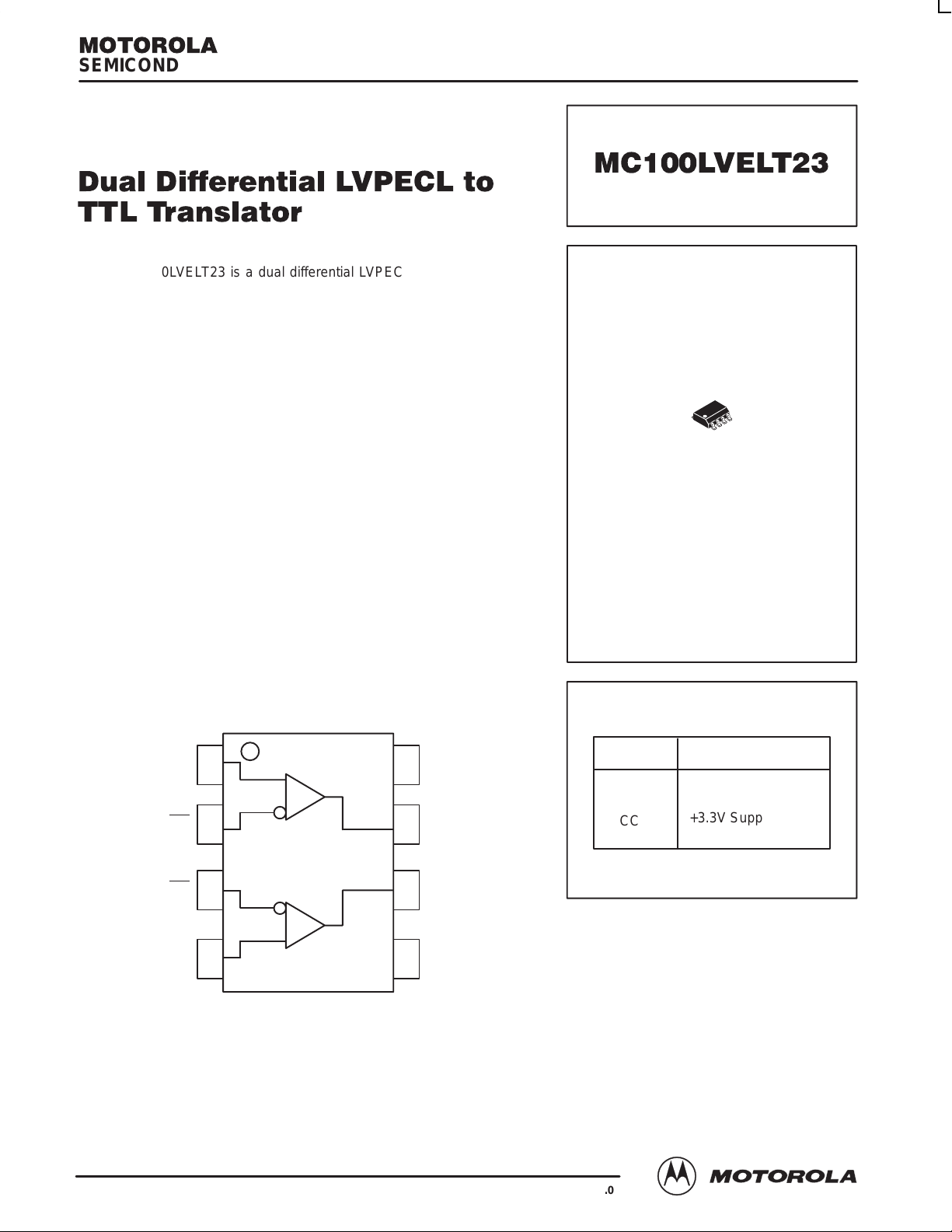
The MC100LVELT23 is a dual differential LVPECL to TTL translator.
Because L VPECL (Positive ECL) levels are used only +3.3V and ground
are required. The small outline 8-lead SOIC package and the dual gate
design of the LVELT23 makes it ideal for applications which require the
translation of a clock and a data signal.
The LVELT23 is available in only the ECL 100K standard. Since there
are no L VPECL outputs or an external VBB reference, the L VELT23 does
not require both ECL standard versions. The LVPECL inputs are
differential; there is no specified difference between the differential input
10H and 100K standards. Therefore, the MC100L VEL T23 can accept any
standard differential LVPECL input referenced from a VCC of 3.3V.
• 2.0ns Typical Propagation Delay
• Differential LVPECL Inputs
• Small Outline SOIC Package
• 24mA TTL Outputs
• Flow Through Pinouts
• ESD Performance: Human Body Model 1200V; Machine Model 150V
Order this document
by MC100LVELT23/D
MC100LVELT23
D SUFFIX
8–LEAD PLASTIC SOIC PACKAGE
CASE 751–06
Note:
1) Pulling the output higher than VCC is not recommended. Doing so
causes excessive leakage and possible latchup leading to reliability
risk.
D0
D0
1
2
V
78Q0
CC
LVPECL TTL
3
45
D1
Figure 1. 8–Lead Pinout and Logic Diagram
6
Q1D1
GND
PIN DESCRIPTION
PIN FUNCTION
Qn TTL Outputs
Dn Diff LVPECL Inputs
V
CC
GND Ground
+3.3V Supply
8/99
Motorola, Inc. 1999
3–1
REV 1.0
MC100LVELT23
MAXIMUM RATINGS*
Symbol Parameter Value Unit
V
CC
T
A
T
STG
Θ Thermal Resistnace Through Package (No Air Flow) 130 °C/W
* Maximum Ratings are those values beyond which damage to the device may occur. Functional operation should be restricted to the
Recommended Operating Conditions.
TTL OUTPUT DC CHARACTERISTICS (VCC = 3.0V to 3.6V; TA = –40°C to 85°C)
Symbol Characteristic Min Typ Max Unit Condition
V
OH
V
OL
I
CCH
I
CCL
I
OS
DC Supply Voltage (Referenced to GND) –0.5 to +3.8 V
Operating Temperature Range (In Free-Air) –40 to 85 °C
Storage Temperature Range –55 to +150 °C
Output HIGH Voltage 2.0 V IOH = –3.0mA
Output LOW Voltage 0.5 V IOL = 24mA
Power Supply Current 20 26 mA
Power Supply Current 28 37 mA
Output Short Circuit Current –80 –130 mA
PECL INPUT DC CHARACTERISTICS (VCC = 3.0V to 3.6V; TA = –40°C to 85°C)
–40°C 0°C 25°C 85°C
Symbol Characteristic Min Max Min Max Min Typ Max Min Max Unit Condition
I
IH
I
IL
V
CMR
V
PP
1. 200mV input guarantees full logic swing at the output.
Input HIGH Current 150 150 150 150 µA
Input LOW Current D0, D1
D0
Common Mode Range 1.2 V
Minimum Peak-to-Peak Input 100 100 100 100 mV Note 1.
, D1
–100
–100
CC
–100
–100
1.2 V
–100
–100
CC
1.2 V
CC
–100
–100
1.2 V
CC
µA
V
AC CHARACTERISTICS (VCC = 3.0V to 3.6V; TA = –40°C to +85°C)
–40°C 0°C 25°C 85°C
Symbol Characteristic Min Typ Max Min Typ Max Min Typ Max Min Typ Max Unit
t
PLH
t
PHL
f
max
t
skpp
t
sk++
t
sk– –
tr, t
2. CL = 20pF.
Propagation Delay (Note 2.) 1.0 1.7 3.0 1.0 1.7 3.0 1.0 1.7 3.0 1.0 1.7 3.0 ns
Propagation Delay (Note 2.) 1.0 1.4 3.0 1.0 1.4 3.0 1.0 1.4 3.0 1.0 1.4 3.0 ns
Max Input Frequency (Note 2.) 275 275 275 275 MHz
Part–to–Part Skew (Note 2.) 0.5 0.5 0.5 0.5 ns
Output–to–Output Skew 60 60 60 110 ps
Output–to–Output Skew 25 25 25 25 ps
Output Rise/Fall 330 700 330 700 330 700 330 700 ps
f
MOTOROLA ECLinPS and ECLinPS Lite
3–2
DL140 — Rev 3
 Loading...