MOTOROLA MC10E337, MC100E337 Technical data

MC100E337
MOTOROLA
SEMICONDUCTOR TECHNICAL DATA
3 Bit Scannable Registered
Bus Transceiver
The MC10E/100E337 is a 3-bit registered bus transceiver with scan. The bus outputs (BUS0±BUS2) are specified for driving a 25Ω bus; the receive outputs (Q0 ± Q2) are specified for 50Ω. The bus outputs feature a normal HIGH level (VOH) and a cutoff LOW level Ð when LOW , the outputs go to ± 2.0V and the output emitter-follower is ªoffº, presenting a high impedance to the bus. The bus outputs also feature edge slow-down capacitors.
•Scannable Version of E336
•25Ω Cutoff Bus Outputs
•50Ω Receiver Outputs
•Scannable Registers
•Sync. and Async. Bus Enables
•Non-inverting Data Path
•1500ps Max. Clock to Bus (Data Transmit)
•1000ps Max. Clock to Q (Data Receive)
•Bus Outputs Feature Internal Edge Slow-Down Capacitors
•Additional Package Ground Pins
•Extended 100E VEE Range of ± 4.2V to ± 5.46V
•75kΩ Input Pulldown Resistors
MC10E337
MC100E337
3-BIT SCANNABLE
REGISTERED
BUS TRANSCEIVER
FN SUFFIX
PLASTIC PACKAGE
CASE 776-02
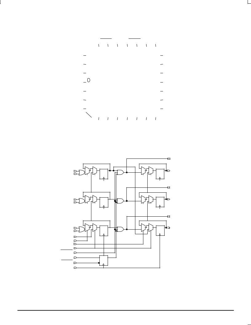
Both drive and receive sides feature the same logic, including a loopback path to hold data. The HOLD/LOAD function is controlled by Transmit Enable (TEN) and Receive Enable (REN) on the transmit and receive sides respectively, with a HIGH selecting LOAD. Note that the implementation of the E337 Receive Enable differs from that of the E336.
A synchronous bus enable (SBUSEN) is provided for normal, non-scan operation. The asynchronous bus disable (ABUSDIS) disables the bus immediately for scan mode.
The SYNCEN input is provided for flexibility when re-enabling the bus after disabling with ABUSDIS, allowing either synchronous or asynchronous re-enabling. An alternative use is asynchronous-only operation with ABUSDIS, in which case SYNCEN is tied LOW, or left open. SYNCEN is implemented as an overriding SET control (active-LOW) to the enable flip-flop.
Scan mode is selected by a HIGH at the SCAN input. Scan input data is shifted in through S_IN and output data appears at the Q2 output.
All registers are clocked on the positive transition of CLK. Additional lead-frame grounding is provided through the Ground pins (GND) which should be connected to 0V. The GND pins are not electrically connected to the chip.
PIN NAMES
|
|
Pin |
Function |
|
|
|
|
|
|
|
|
|
|
A0 ± A2 |
Data Inputs A |
|
|
|
|
B0 ± B2 |
Data Inputs B |
|
|
|
|
S-IN |
Serial (Scan) Data Input |
|
|
|
|
TEN, REN |
HOLD/LOAD Controls |
|
|
|
|
SCAN |
|
Scan Control |
|
|
|
ABUSDIS |
Asynchronous Bus Disable |
|
|
|
|
SBUSEN |
Synchronous Bus Enable |
|
|
|
|
SYNCEN |
Synchronous Enable Control |
|
|
|
|
CLK |
Clock |
|
|
|
|
BUS0 ± BUS2 |
25Ω Cutoff Bus Outputs |
|
|
|
|
Q0 ± Q2 |
Receive Data Outputs (Q2 serves as SCAN_OUT in scan mode) |
|
|
12/93 |
|
|
|
||
Motorola, Inc. 1996 |
REV 2 |
||||

MC10E337 MC100E337
Pinout: 28-Lead PLCC (Top View)
|
|
SBUSEN SYNCEN |
B0 |
|
A0 ABUSDIS VCCO |
Q0 |
|
||||||||||||||
|
|
|
|
|
|
|
|
|
|
|
|
|
|
|
|
|
|
|
|
|
|
|
|
|
25 |
24 |
|
23 |
22 |
|
21 |
|
20 |
|
19 |
|
|
|
|||||
SCAN |
|
26 |
|
|
|
|
|
|
|
|
|
|
|
|
|
|
|
18 |
|
GND |
|
S-IN |
|
27 |
|
|
|
|
|
|
|
|
|
|
|
|
|
|
|
17 |
|
BUS0 |
|
|
|
|
|
|
|
|
|
|
|
|
|
|
|
|
|
|
|||||
TEN |
|
28 |
|
|
|
|
|
|
|
|
|
|
|
|
|
|
|
16 |
|
VCC |
|
|
|
|
|
|
|
|
|
|
|
|
|
|
|
|
|
|
|||||
VEE |
|
1 |
|
|
|
|
|
|
|
|
|
|
|
|
|
|
|
15 |
|
Q1 |
|
|
|
|
|
|
|
|
|
|
|
|
|
|
|
|
|
|
|||||
REN |
|
2 |
|
|
|
|
|
|
|
|
|
|
|
|
|
|
|
14 |
|
VCCO |
|
|
|
|
|
|
|
|
|
|
|
|
|
|
|
|
|
|
|||||
CLK |
|
3 |
|
|
|
|
|
|
|
|
|
|
|
|
|
|
|
13 |
|
BUS1 |
|
|
|
|
|
|
|
|
|
|
|
|
|
|
|
|
|
|
|||||
A1 |
|
4 |
|
|
|
|
|
|
|
|
|
|
|
|
|
|
|
12 |
|
GND |
|
|
|
|
|
|
|
|
|
|
|
|
|
|
|
|
|
|
|||||
|
|
|
5 |
6 |
|
7 |
8 |
|
9 |
|
10 |
|
11 |
|
|
|
|||||
|
|
|
|
|
|
|
|
|
|||||||||||||
|
|
|
|
|
|
|
|
|
|
|
|
|
|
|
|
|
|
|
|
|
|
|
|
|
|
|
|
|
|
|
|
|
|
|
|
|
|
|
|
|
|
|
|
|
|
|
|
B1 |
|
A2 |
B2 |
VCCO |
BUS2 |
GND |
Q2 |
|
|||||||||
|
* All VCC and VCCO pins are tied together on the die. |
|
|||||||||||||||||||
|
|
LOGIC DIAGRAM |
|
|
|
|
BUS2 |
A2 |
D Q |
D Q |
Q2/ |
B2 |
|
|
SCAN_OUT |
|
|
|
BUS1 |
A1 |
D Q |
D Q |
Q1 |
B1 |
|
|
|
|
|
|
BUS0 |
A0 |
D Q |
D Q |
Q0 |
B0 |
|
|
|
S_IN |
|
|
|
TEN |
|
|
|
REN |
|
|
|
SCAN |
|
|
|
ABUSDIS |
|
|
|
SBUSEN |
D Q |
|
|
SYNCEN |
SET |
|
|
|
|
|
|
CLK |
|
|
|
MOTOROLA |
2±2 |
 Loading...