MOTOROLA MC10EL05, MC100EL05 Technical data

MOTOROLA
SEMICONDUCTOR TECHNICAL DATA
2 Input Differential AND/NAND
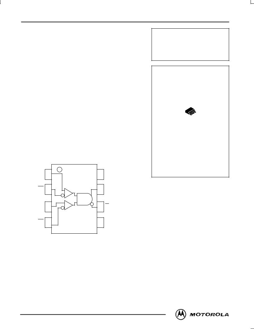
The MC10EL/100EL05 is a 2-input differential AND/NAND gate. The device is functionally equivalent to the E404 device with higher performance capabilities. With propagation delays and output transition times significantly faster than the E404 the EL05 is ideally suited for those applications which require the ultimate in AC performance.
Because a negative 2-input NAND is equivalent to a 2-input OR function, the differential inputs and outputs of the device allows the EL05 to also be used as a 2-input differential OR/NOR gate.
The differential inputs employ clamp circuitry so that under open input conditions (pulled down to VEE) the input to the AND gate will be HIGH. In this way, if one set of inputs is open, the gate will remain active to the other input.
•275ps Propagation Delay
•High Bandwidth Output Transitions
•75kΩ Internal Input Pulldown Resistors
•>1000V ESD Protection
LOGIC DIAGRAM AND PINOUT ASSIGNMENT
D0 |
1 |
8 |
VCC |
D0 |
2 |
7 |
Q |
D1 |
3 |
6 |
Q |
D1 |
4 |
5 |
VEE |
MC10EL05
MC100EL05
8 

1
D SUFFIX
PLASTIC SOIC PACKAGE
CASE 751-05
|
|
PIN DESCRIPTION |
||
|
|
|
|
|
|
PIN |
|
FUNCTION |
|
|
|
|
|
|
|
D0, D1 |
|
Data Inputs |
|
|
Q |
|
Data Outputs |
|
|
|
|
|
|
|
|
|
|
|
12/93
Motorola, Inc. 1996 |
REV 2 |

MC10EL05 MC100EL05
DC CHARACTERISTICS (VEE = VEE(min) to VEE(max); VCC = GND)
|
|
|
±40°C |
|
|
0°C |
|
|
25°C |
|
|
85°C |
|
|
|
|
|
|
|
|
|
|
|
|
|
|
|
|
|
Symbol |
Characteristic |
Min |
Typ |
Max |
Min |
Typ |
Max |
Min |
Typ |
Max |
Min |
Typ |
Max |
Unit |
|
|
|
|
|
|
|
|
|
|
|
|
|
|
|
IEE |
Power Supply Current |
|
|
|
|
|
|
|
|
|
|
|
|
|
|
10EL |
|
18 |
22 |
|
18 |
22 |
|
18 |
22 |
|
18 |
22 |
|
|
100EL |
|
18 |
22 |
|
18 |
22 |
|
18 |
22 |
|
21 |
25 |
mA |
|
|
|
|
|
|
|
|
|
|
|
|
|
|
|
VEE |
Power Supply Voltage |
|
|
|
|
|
|
|
|
|
|
|
|
|
|
10EL |
±4.75 |
±5.2 |
±5.5 |
±4.75 |
±5.2 |
±5.5 |
±4.75 |
±5.2 |
±5.5 |
±4.75 |
±5.2 |
±5.5 |
|
|
100EL |
±4.20 |
±4.5 |
±5.5 |
±4.20 |
±4.5 |
±5.5 |
±4.20 |
±4.5 |
±5.5 |
±4.20 |
±4.5 |
±5.5 |
V |
|
|
|
|
|
|
|
|
|
|
|
|
|
|
|
IIH |
Input HIGH Current |
|
|
150 |
|
|
150 |
|
|
150 |
|
|
150 |
μA |
AC CHARACTERISTICS (VEE = VEE(min) to VEE(max); VCC = GND)
|
|
|
±40°C |
|
|
0°C |
|
|
25°C |
|
|
85°C |
|
|
|
|
|
|
|
|
|
|
|
|
|
|
|
|
|
Symbol |
Characteristic |
Min |
Typ |
Max |
Min |
Typ |
Max |
Min |
Typ |
Max |
Min |
Typ |
Max |
Unit |
|
|
|
|
|
|
|
|
|
|
|
|
|
|
|
tPLH |
Propagation Delay to |
135 |
260 |
440 |
185 |
275 |
390 |
185 |
275 |
390 |
215 |
305 |
420 |
ps |
tPHL |
Output |
|||||||||||||
V |
Minimum Input Swing1 |
150 |
|
|
150 |
|
|
150 |
|
|
150 |
|
|
mV |
PP |
|
|
|
|
|
|
|
|
|
|
|
|
|
|
V |
Common Mode Range2 |
±0.4 |
|
See2 |
±0.4 |
|
See2 |
±0.4 |
|
See2 |
±0.4 |
|
See2 |
V |
CMR |
|
|
|
|
|
|
|
|
|
|
|
|
|
|
tr |
Output Rise/Fall Times Q |
100 |
225 |
350 |
100 |
225 |
350 |
100 |
225 |
350 |
100 |
225 |
350 |
ps |
tf |
(20% ± 80%) |
1.Minimum input swing for which AC parameters are guaranteed. The device has a DC gain of ≈40.
2.The CMR range is referenced to the most positive side of the differential input signal. Normal operation is obtained if the HIGH level falls within
the specified range and the peak-to-peak voltage lies between VPPmin and 1V. The lower end of the CMR range is dependent on VEE and is equal to VEE + 3.0V.
MOTOROLA |
3±2 |
 Loading...