


MC10E1651L
SEMICONDUCTOR TECHNICAL DATA
2–1
REV 1
Motorola, Inc. 1996
12/93
The MC10E1651 is functionally and pin-for-pin compatible with the
MC1651 in the MECL III family, but is fabricated using Motorola’s
advanced MOSAIC III process. The MC10E1651 incorporates a fixed
level of input hysteresis as well as output compatibility with 10KH logic
devices. In addition, a latch is available allowing a sample and hold
function to be performed. The device is available in both a 16-pin DIP and
a 20-pin surface mount package.
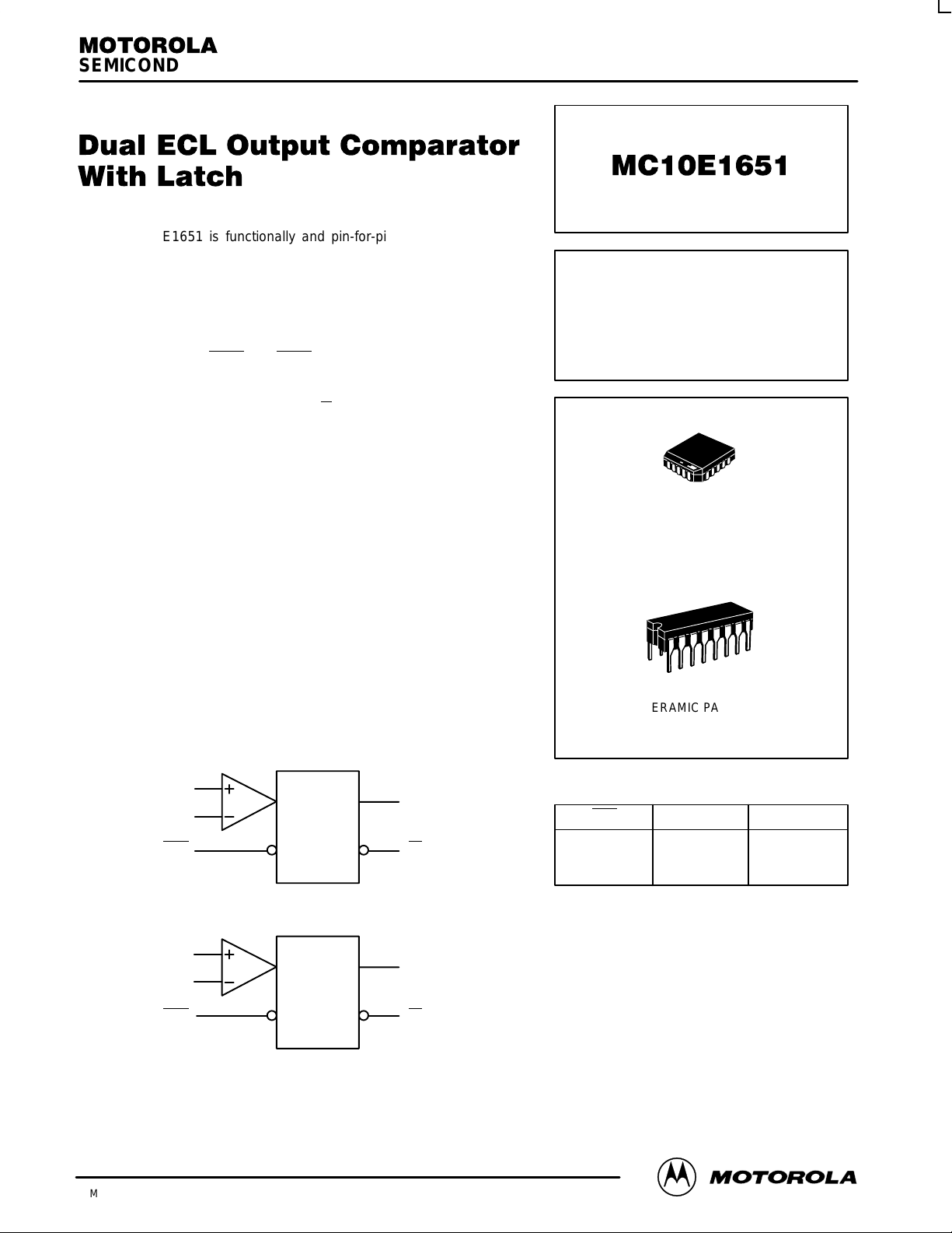
The latch enable (LEN
a
and LEN
b
) input pins operate from standard
ECL 10KH logic levels. When the latch enable is at a logic high level the
MC10E1651 acts as a comparator, hence Q will be at a logic high level if
V1 > V2 (V1 is more positive than V2). Q
is the complement of Q. When
the latch enable input goes to a low logic level, the outputs are latched in
their present state providing the latch enable setup and hold time
constraints are met.
• Typ. 3.0 dB Bandwidth > 1.0 GHz
• Typ. V to Q Propagation Delay of 775 ps
• Typ. Output Rise/Fall of 350 ps
• Common Mode Range –2.0 V to +3.0 V
• Individual Latch Enables
• Differential Outputs
• 28mV Input Hysteresis
Qa
Qa
LEN
a
V2a
V1a
Qb
Qb
LEN
b
V2b
V1b
LOGIC DIAGRAM
V
EE
= –5.2 V
V
CC
= +5.0 V
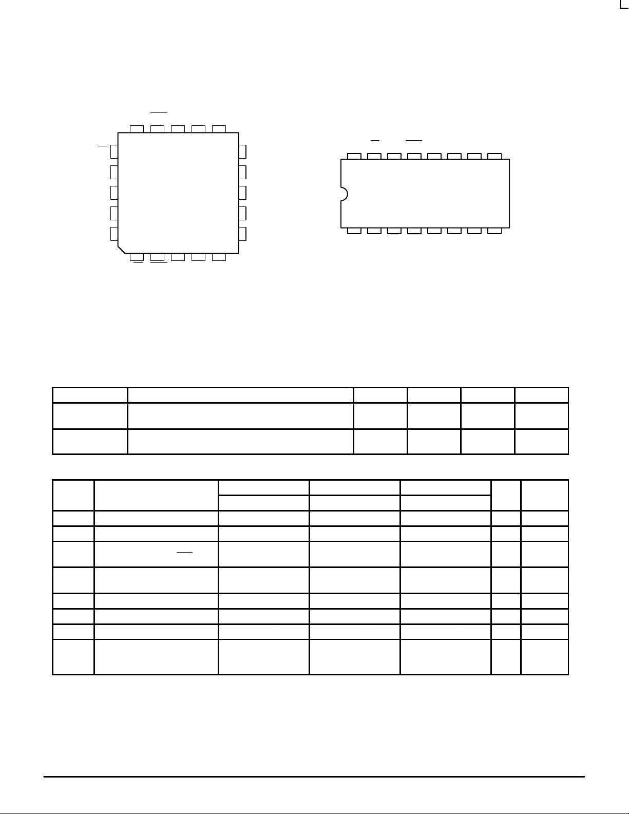
FN SUFFIX
PLASTIC PACKAGE
CASE 775-02
DUAL ECL OUTPUT
COMPARATOR
WITH LATCH
L SUFFIX
CERAMIC PACKAGE
CASE 620-10
FUNCTION TABLE
LEN V1, V2 Function
H
H
L
V1 > V2
V1 < V2
X
H
L
Latched
MC10E1651
MOTOROLA ECLinPS and ECLinPS Lite
DL140 — Rev 4
2–2
Pinout: 20-Lead PLCC (Top View)
Qb
GND
NC
GND
Qa
Qb LEN
b
NC V1b V2b
V
CC
NC
NC
V
EE
V
CC
Qa
LEN
a
NC V2a V1a
Pinout: 16-Pin Ceramic DIP (Top View)
87654321
910111213141516
NCV
CC
V2bV1bLEN
b
QbQbGND
V
EE
V
CC
V1aV2aLEN
a
QaQaGND
19
18
13
17 16 15 14
12
11
10
9
4 5 6 7 8
20
1
2
3
ABSOLUTE MAXIMUM RATINGS (Beyond which device life may be impaired)
Symbol Characteristic Min Typ Max Unit
VSUP Total Supply Voltage
|V
EE
| + |V
CC
|
12.0
V
VPP Differential Input Voltage
|V1 – V2|
3.7
V
DC CHARACTERISTICS (V
EE
= –5.2 V ±5%; V
CC
= +5.0 V ±5%)
0°C 25°C 85°C
Symbol Characteristic Min Typ Max Min Typ Max Min Typ Max Unit Condition
V
OH
Output HIGH Voltage –1020 –840 –980 –810 –920 –735 mV
V
OL
Output Low Voltage –1950 –1630 –1950 –1630 –1950 –1600 mV
II
I
IH
Input Current (V1, V2)
Input HIGH Current (LEN
)
65
150
65
150
65
150
µA
I
CC
I
EE
Positive Supply Current
Negative Supply Current
50
–55
50
–55
50
–55
mA
VCMR Common Mode Range –2.0 3.0 –2.0 3.0 –2.0 3.0 V
Hys Hysteresis 27 27 30 mV
V
skew
Hysteresis Skew –1.0 –1.0 0 mV 1
C
in
Input Capacitance
DIP
PLCC
3
2
3
2
3
2
pF
1. Hysteresis skew (V
skew
) is provided to indicate the offset of the hysteresis window. For example, at 25°C the nominal hysteresis value is 27mV
and the V
skew
value indicates that the hysteresis was skewed from the reference level by 1mV in the negative direction. Hence the hysteresis
window ranged from 14mV below the reference level to 13mV above the reference level. All hysteresis measurements were determined using
a reference voltage of 0mV.
MC10E1651
2–3 MOTOROLAECLinPS and ECLinPS Lite
DL140 — Rev 4
AC CHARACTERISTICS (V
EE
= –5.2 V ±5%; V
CC
= +5.0 V ±5%)
0°C 25°C 85°C
Symbol Characteristic Min Typ Max Min Typ Max Min Typ Max Unit Condition
t
PLH
t
PHL
Propagation Delay to Output
V to Q
LEN
to Q
600
400
750
575
900
750
625
400
775
575
925
750
700
500
850
650
1050
850
ps 1
t
s
Setup Time
V
450 300 450 300 550 350
ps
t
h
Enable Hold Time
V
–50 –250 –50 –250 –100 –250
ps
t
pw
Minimum Pulse Width
LEN
400 400 400
ps
t
skew
Within Device Skew 15 15 15 ps 2
T
DE
Delay Dispersion
(ECL Levels)
100
60
ps
3, 4
3, 5
T
DL
Delay Dispersion
(TTL Levels)
350
100
ps
6, 7
5, 6
t
r
t
f
Rise/Fall Times
20-80%
225 325 475 225 325 475 250 375 500
ps
1. The propagation delay is measured from the crosspoint of the input signal and the threshold value to the crosspoint of the Q and Q output signals.
For propagation delay measurements the threshold level (V
THR
) is centered about an 850mV input logic swing with a slew rate of 0.75 V/NS.
There is an insignificant change in the propagation delay over the input common mode range.
2. t
skew
is the propagation delay skew between comparator A and comparator B for a particular part under identical input conditions.
3. Refer to figure 4 and note that the input is at 850mV ECL levels with the input threshold range between the 20% and 80% points. The delay
is measured from the crosspoint of the input signal and the threshold value to the crosspoint of the Q and Q
output signals.
4. The slew rate is 0.25 V/NS for input rising edges.
5. The slew rate is 0.75 V/NS for input rising edges.
6. Refer to Figure 5 and note that the input is at 2.5 V TTL levels with the input threshold range between the 20% and 80% points. The delay is
measured from the crosspoint of the input signal and the threshold value to the crosspoint of the Q and Q
output signals.
7. The slew rate is 0.3 V/NS for input rising edges.
APPLICATIONS INFORMATION
The timing diagram (Figure 3) is presented to illustrate the
MC10E1651’s compare and latch features. When the signal
on the LEN
pin is at a logic high level, the device is operating
in the “compare mode,” and the signal on the input arrives at
the output after a nominal propagation delay (t
PHL
, t
PLH
). The
input signal must be asserted for a time, t
s
, prior to the
negative going transition on LEN and held for a time, t
h
, after
the LEN transition. After time t
h
, the latch is operating in the
“latch mode,” thus transitions on the input do not appear at
the output. The device continues to operate in the “latch
mode” until the latch is asserted once again. Moreover, the
LEN
pulse must meet the minimum pulse width (t
pw
)
requirement to effect the correct input-output relationship.
Note that the LEN waveform in Figure 3 shows the LEN
signal swinging around a reference labeled VBB
INT
; this
waveform emphasizes the requirement that LEN
follow
typical ECL 10KH logic levels because VBB
INT
is the
internally generated reference level, hence is nominally at
the ECL VBB level.
Finally, V
OD
is the input voltage overdrive and represents
the voltage level beyond the threshold level (V
THR
) to which
the input is driven. As an example, if the threshold level is set
on one of the comparator inputs as 80mV and the input signal
swing on the complementary input is from zero to 100mV , the
positive going overdrive would be 20mV and the negative
going overdrive would be 80mV. The result of differing
overdrive levels is that the devices have shorter propagation
delays with greater overdrive because the threshold level is
crossed sooner than the case of lower overdrive levels.
Typically, semiconductor manufactures refer to the threshold
voltage as the input offset voltage (VOS) since the threshold
voltage is the sum of the externally supplied reference
voltage and inherent device offset voltage.
 Loading...