


TEXAS INSTRUMENTS TPS73201, TPS73215, TPS73216, TPS73218, TPS73225 Technical data
...TPS73201
www.ti.com
TPS73201, TPS73215, TPS73216
TPS73218, TPS73225, TPS73230
TPS73233, TPS73250
SBVS037F –AUGUST 2003 –REVISED SEPTEMBER 2004
Cap-Free, NMOS, 250mA Low Dropout Regulator
with Reverse Current Protection
FEATURES
∙Stable with No Output Capacitor or Any Value or Type of Capacitor
∙Input Voltage Range: 1.7V to 5.5V
∙Ultralow Dropout Voltage: 40mV Typ at 250mA
∙Excellent Load Transient Response—with or without Optional Output Capacitor
∙New NMOS Topology Provides Low Reverse Leakage Current
∙Low Noise: 30µV RMS Typ (10kHz to 100kHz)
∙0.5% Initial Accuracy
∙1% Overall Accuracy (Line, Load, and Temperature)
∙Less Than 1µA Max IQ in Shutdown Mode
∙Thermal Shutdown and Specified Min/Max Current Limit Protection
∙Available in Multiple Output Voltage Versions
–Fixed Outputs of 1.2V, 1.5V, 1.6V, 1.8V, 2.5V, 3.0V, 3.3V, and 5.0V
–Adjustable Outputs From 1.20V to 5.5V
–Custom Outputs Available
APPLICATIONS
∙Portable/Battery-Powered Equipment
∙Post-Regulation for Switching Supplies
∙Noise-Sensitive Circuitry such as VCOs
∙Point of Load Regulation for DSPs, FPGAs, ASICs, and Microprocessors
DESCRIPTION
The TPS732xx family of low-dropout (LDO) voltage regulators uses a new topology: an NMOS pass element in a voltage-follower configuration. This topology is stable using output capacitors with low ESR, and even allows operation without a capacitor. It also provides high reverse blockage (low reverse current) and ground pin current that is nearly constant over all values of output current.
The TPS732xx uses an advanced BiCMOS process to yield high precision while delivering very low dropout voltages and low ground pin current. Current consumption, when not enabled, is under 1µA and ideal for portable applications. The extremely low output noise (30µVRMS with 0.1µF CNR) is ideal for powering VCOs. These devices are protected by thermal shutdown and foldback current limit.
|
|
|
|
|
|
|
|
|
|
|
DCQ PACKAGE |
||||||||||||||
|
|
|
|
|
|
|
|
|
|
|
|
|
SOT223 |
|
|
|
|
|
|||||||
|
|
DBV PACKAGE |
|
|
|
|
|
(TOP VIEW) |
|
|
|
|
|
||||||||||||
|
|
|
|
|
|
|
|
|
|
|
|
|
|
|
|
|
|
|
|
|
|||||
|
|
|
|
SOT23 |
|
|
|
|
|
|
|
|
|
|
|
|
|
|
|
|
|
|
|
||
|
|
|
|
|
|
|
|
|
|
|
|
|
|
|
|
|
|
|
|
|
|
|
|||
|
|
|
(TOP VIEW) |
|
|
|
|
|
|
|
|
|
|
|
|
|
|
TAB IS GND |
|||||||
|
|
|
|
|
|
|
|
|
|
|
|
|
|
|
|
|
|
|
|
|
|
|
|
|
|
IN |
|
|
1 |
5 |
|
|
OUT |
|
|
|
|
|
|
|
|
|
|
|
|
|
|
|
|
|
|
|
|
|
|
|
|
|
|
|
|
|
|
|
|
|
|
|
|
|
|
|
|
||||
GND |
|
|
2 |
|
|
|
|
1 |
|
2 |
|
3 |
4 |
|
5 |
|
|
||||||||
|
|
|
|
|
|
|
|
|
|
|
|||||||||||||||
EN |
|
|
3 |
4 |
|
|
NR/FB |
|
|
|
|
|
|
|
|
|
|
|
|
|
|
|
|
|
|
|
|
|
|
|
|
|
|
|
|
|
|
|
|
|
|
|
|
|
|
|
|||||
|
|
|
|
|
|
|
|
|
|
|
|
|
|
|
|
|
|
|
|
|
|||||
|
|
|
|
|
|
|
|
IN |
|
|
|
GND |
|
EN |
|||||||||||
|
|
|
|
|
|
|
|
|
|
|
|
OUT |
|
|
|
NR/FB |
|||||||||
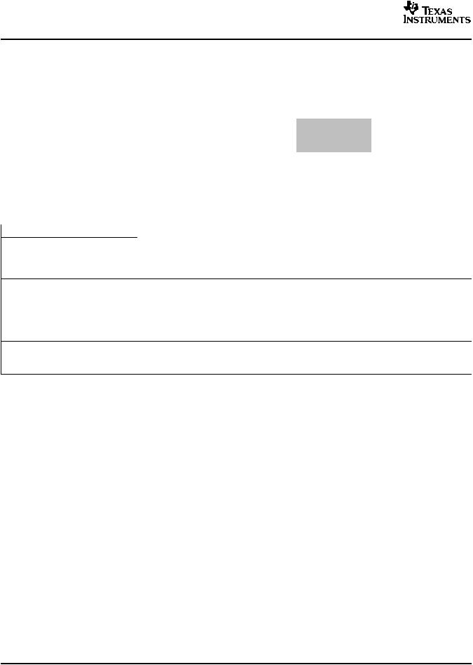
|
Optional |
|
Optional |
VIN |
IN |
OUT |
VOUT |
|
|
TPS732xx |
|
|
EN |
GND NR |
|
Optional
Typical Application Circuit for Fixed-Voltage Versions
Please be aware that an important notice concerning availability, standard warranty, and use in critical applications of Texas Instruments semiconductor products and disclaimers thereto appears at the end of this data sheet.
PRODUCTION DATA information is current as of publication date. |
Copyright © 2003–2004, Texas Instruments Incorporated |
Products conform to specifications per the terms of the Texas |
|
Instruments standard warranty. Production processing does not |
|
necessarily include testing of all parameters. |
|

TPS73201, TPS73215, TPS73216 |
|
|
TPS73218, TPS73225, TPS73230 |
|
|
TPS73233, TPS73250 |
www.ti.com |
|
SBVS037F –AUGUST 2003 –REVISED SEPTEMBER 2004 |
||
|
This integrated circuit can be damaged by ESD. Texas Instruments recommends that all integrated circuits be handled with appropriate precautions. Failure to observe proper handling and installation procedures can cause damage.
ESD damage can range from subtle performance degradation to complete device failure. Precision integrated circuits may be more susceptible to damage because very small parametric changes could cause the device not to meet its published specifications.
ORDERING INFORMATION
PRODUCT VOUT (1)
TPS73201 |
Adjustable |
||
or 1.2V |
(3) |
||
|
|||
TPS73215 1.5V
TPS73216 1.6V
TPS73218 1.8V
TPS73225 2.5V
TPS73230 3.0V
TPS73233 3.3V
TPS73250 5.0V
PACKAGE-LEAD |
SPECIFIED |
PACKAGE |
ORDERING |
|
|
TEMPERATURE |
TRANSPORT MEDIA, |
||||
(DESIGNATOR)(2) |
MARKING |
NUMBER |
|||
RANGE |
QUANTITY |
||||
|
|
|
|||
SOT23-5 (DBV) |
-40°C to +125°C |
PJEQ |
TPS73201DBVT |
Tape and Reel, 250 |
|
TPS73201DBVR |
Tape and Reel, 3000 |
||||
|
|
|
|||
SOT223-5 (DCQ) |
-40°C to +125°C |
PS73201 |
TPS73201DCQT |
Tube, 80 |
|
TPS73201DCQR |
Tape and Reel, 2500 |
||||
|
|
|
|||
SOT23-5 (DBV) |
-40°C to +125°C |
T38 |
TPS73215DBVT |
Tape and Reel, 250 |
|
TPS73215DBVR |
Tape and Reel, 3000 |
||||
|
|
|
|||
SOT223-5 (DCQ) |
-40°C to +125°C |
PS73215 |
TPS73215DCQT |
Tube, 80 |
|
TPS73215DCQR |
Tape and Reel, 2500 |
||||
|
|
|
|||
SOT23-5 (DBV) |
-40°C to +125°C |
T50 |
TPS73216DBVT |
Tape and Reel, 250 |
|
TPS73216DBVR |
Tape and Reel, 3000 |
||||
|
|
|
|||
SOT23-5 (DBV) |
-40°C to +125°C |
T37 |
TPS73218DBVT |
Tape and Reel, 250 |
|
TPS73218DBVR |
Tape and Reel, 3000 |
||||
|
|
|
|||
SOT223-5 (DCQ) |
-40°C to +125°C |
PS73218 |
TPS73218DCQT |
Tube, 80 |
|
TPS73218DCQR |
Tape and Reel, 2500 |
||||
|
|
|
|||
SOT23-5 (DBV) |
-40°C to +125°C |
T36 |
TPS73225DBVT |
Tape and Reel, 250 |
|
TPS73225DBVR |
Tape and Reel, 3000 |
||||
|
|
|
|||
SOT223-5 (DCQ) |
-40°C to +125°C |
PS73225 |
TPS73225DCQT |
Tube, 80 |
|
TPS73225DCQR |
Tape and Reel, 2500 |
||||
|
|
|
|||
SOT23-5 (DBV) |
-40°C to +125°C |
T39 |
TPS73230DBVT |
Tape and Reel, 250 |
|
TPS73230DBVR |
Tape and Reel, 3000 |
||||
|
|
|
|||
SOT223-5 (DCQ) |
-40°C to +125°C |
PS73230 |
TPS73230DCQT |
Tube, 80 |
|
TPS73230DCQR |
Tape and Reel, 2500 |
||||
|
|
|
|||
SOT23-5 (DBV) |
-40°C to +125°C |
T40 |
TPS73233DBVT |
Tape and Reel, 250 |
|
TPS73233DBVR |
Tape and Reel, 3000 |
||||
|
|
|
|||
SOT223-5 (DCQ) |
-40°C to +125°C |
PS73233 |
TPS73233DCQT |
Tube, 80 |
|
TPS73233DCQR |
Tape and Reel, 2500 |
||||
|
|
|
|||
SOT23-5 (DBV) |
-40°C to +125°C |
T41 |
TPS73250DBVT |
Tape and Reel, 250 |
|
TPS73250DBVR |
Tape and Reel, 3000 |
||||
|
|
|
|||
SOT223-5 (DCQ) |
-40°C to +125°C |
PS73250 |
TPS73250DCQT |
Tube, 80 |
|
TPS73250DCQR |
Tape and Reel, 2500 |
||||
|
|
|
(1)Custom output voltages from 1.3V to 4V in 100mV increments are available on a quick-turn basis for prototyping. Production quantities are available; minimum order quantities apply. Contact factory for details and availability.
(2)For the most current specification and package information, refer to the Package Option Addendum located at the end of this datasheet.
(3)For fixed 1.2V operation, tie FB to OUT.
2
|
TPS73201, TPS73215, TPS73216 |
||
|
TPS73218, TPS73225, TPS73230 |
||
www.ti.com |
|
TPS73233, TPS73250 |
|
SBVS037F –AUGUST 2003 –REVISED SEPTEMBER 2004 |
|||
|
|||
ABSOLUTE MAXIMUM RATINGS |
|
|
|
over operating junction temperature range unless otherwise noted(1) |
|
|
|
|
TPS732xx |
UNIT |
|
VIN range |
-0.3 to 6.0 |
V |
|
VEN range |
-0.3 to 6.0 |
V |
|
VOUT range |
-0.3 to 5.5 |
V |
|
Peak output current |
Internally limited |
|
|
Output short-circuit duration |
Indefinite |
|
|
Continuous total power dissipation |
See Dissipation Ratings Table |
||
Junction temperature range, TJ |
-55 to +150 |
°C |
|
Storage temperature range |
-65 to +150 |
°C |
|
ESD rating, HBM |
2 |
kV |
|
ESD rating, CDM |
500 |
V |
|
(1)Stresses beyond those listedunder absolute maximum ratingsmay cause permanent damage to the device. These are stress ratings only, andfunctional operation of the device at these or any other conditions beyondthose indicated under the Electrical Characteristics is not implied. Exposureto absolute maximum rated conditions for extended periods may affect devicereliability.
POWER DISSIPATION RATINGS(1)
BOARD |
PACKAGE |
RΘJC |
RΘJA |
DERATING FACTOR |
TA ≤ 25°C |
TA = 70°C |
TA = 85°C |
|
ABOVE TA = 25°C |
POWER RATING |
POWER RATING |
POWER RATING |
|||||
|
|
|
|
|||||
Low-K(2) |
DBV |
64°C/W |
255°C/W |
3.9mW/°C |
390mW |
215mW |
155mW |
|
High-K (3) |
DBV |
64°C/W |
180°C/W |
5.6mW/°C |
560mW |
310mW |
225mW |
|
Low-K(2) |
DCQ |
15°C/W |
53°C/W |
18.9mW/°C |
1.89W |
1.04W |
0.76W |
(1)SeePower Dissipation in theApplications section formore information related to thermal design.
(2)The JEDEC Low-K (1s) boarddesign used to derive this data was a 3 inch x 3 inch, two-layer board with2-ounce copper traces on top of the board.
(3)The JEDEC High-K (2s2p)board design used to derive this data was a 3 inch x 3 inch, multilayer boardwith 1-ounce internal power and ground planes and 2-ounce copper traces on thetop and bottom of the board.
3
TPS73201, TPS73215, TPS73216 |
|
|
TPS73218, TPS73225, TPS73230 |
|
|
TPS73233, TPS73250 |
www.ti.com |
|
SBVS037F –AUGUST 2003 –REVISED SEPTEMBER 2004 |
||
|
ELECTRICAL CHARACTERISTICS
Over operating temperature range (TJ = -40°C to +125°C), VIN = VOUT(nom) + 0.5V(1), IOUT = 10mA, VEN = 1.7V, and COUT = 0.1µF, unless otherwise noted. Typical values are at TJ = 25°C.
|
|
PARAMETER |
V |
|
Input voltage range(1) |
IN |
|
|
VFB |
|
Internal reference (TPS73201) |
|
|
Output voltage range (TPS73201)(2) |
VOUT |
|
Nominal |
|
Accuracy(1) |
|
|
|
VIN, IOUT, and T |
V %/ |
V |
Line regulation(1) |
OUT |
IN |
|
VOUT%/ |
IOUT |
Load regulation |
VDO |
|
Dropout voltage(3) |
|
(VIN = VOUT (nom) - 0.1V) |
|
|
|
|
ZO(DO) |
|
Output impedance in dropout |
ICL |
|
Output current limit |
ISC |
|
Short-circuit current |
I |
|
Reverse leakage current(4) (-I ) |
REV |
|
IN |
IGND |
|
Ground pin current |
ISHDN |
|
Shutdown current (IGND) |
IFB |
|
FB pin current (TPS73201) |
PSRR |
|
Power-supply rejection ratio |
|
(ripple rejection) |
|
|
|
|
VN |
|
Output noise voltage |
|
BW = 10Hz - 100kHz |
|
tSTR |
|
Startup time |
VEN(HI) |
|
Enable high (enabled) |
VEN(LO) |
|
Enable low (shutdown) |
IEN(HI) |
|
Enable pin current (enabled) |
TSD |
|
Thermal shutdown temperature |
TJ |
|
Operating junction temperature |
TEST CONDITIONS |
MIN |
TYP |
MAX |
UNIT |
|
|
|
1.7 |
|
5.5 |
V |
TJ = 25°C |
|
1.198 |
1.20 |
1.210 |
V |
|
|
VFB |
|
5.5-VDO |
V |
TJ = 25°C |
|
-0.5 |
|
+0.5 |
|
VOUT + 0.5V ≤ VIN ≤ 5.5V; |
-1.0 |
±0.5 |
+1.0 |
% |
|
|
|||||
10 mA ≤ IOUT≤ 250mA |
|
|
|
|
|
VOUT(nom) + 0.5V ≤ VIN ≤ 5.5V |
|
0.01 |
|
%/V |
|
1mA ≤ IOUT ≤ 250mA |
|
0.002 |
|
%/mA |
|
10mA ≤ IOUT ≤ 250mA |
|
0.0005 |
|
||
|
|
|
|||
IOUT = 250mA |
|
|
40 |
150 |
mV |
1.7 V ≤ VIN ≤ VOUT + VDO |
|
0.25 |
|
Ω |
|
VOUT = 0.9 × VOUT(nom) |
250 |
425 |
600 |
mA |
|
VOUT = 0V |
|
|
300 |
|
mA |
VEN ≤ 0.5V, 0V≤ VIN ≤ VOUT |
|
0.1 |
10 |
µA |
|
IOUT = 10mA (IQ) |
|
400 |
550 |
µA |
|
IOUT = 250mA |
|
|
650 |
950 |
|
|
|
|
|||
VEN ≤ 0.5V, VOUT ≤ VIN ≤ 5.5 |
|
0.02 |
1 |
µA |
|
|
|
|
.1 |
.3 |
µA |
f = 100Hz, IOUT = 250 mA |
|
58 |
|
dB |
|
f = 10kHz, IOUT = 250 mA |
|
37 |
|
||
|
|
|
|||
COUT = 10µF, No CNR |
|
27 × VOUT |
|
µVRMS |
|
COUT= 10µF, CNR = 0.01µF |
|
8.5 × VOUT |
|
||
|
|
|
|||
VOUT = 3V, RL = 30Ω |
|
600 |
|
µs |
|
COUT = 1 µF, CNR= 0.01 µF |
|
|
|
|
|
|
|
1.7 |
|
VIN |
V |
|
|
0 |
|
0.5 |
V |
VEN = 5.5V |
|
|
0.02 |
0.1 |
µA |
Shutdown |
Temp increasing |
|
160 |
|
°C |
Reset |
Temp decreasing |
|
140 |
|
|
|
|
|
|||
|
|
-40 |
|
125 |
°C |
(1)Minimum VIN = VOUT +VDO or 1.7V, whichever isgreater.
(2)TPS73201 is tested atVOUT = 2.5V.
(3)VDO is not measured for the TPS73214, TPS73215 orTPS73216 since minimum VIN =1.7V.
(4)Fixed-voltage versions only;refer to Applicationssection for more information.
4

TPS73201, TPS73215, TPS73216
TPS73218, TPS73225, TPS73230
TPS73233, TPS73250
www.ti.com
SBVS037F –AUGUST 2003 –REVISED SEPTEMBER 2004
FUNCTIONAL BLOCK DIAGRAMS
|
|
IN |
|
Charge |
|
|
Pump |
|
EN |
Thermal |
|
|
|
|
|
Protection |
|
|
Ref |
|
|
Servo |
|
|
27kΩ |
|
|
Bandgap |
|
|
Error |
|
|
Amp |
|
|
Current |
|
|
Limit |
OUT |
GND |
8kΩ |
|
|
R1 |
|
|
|
|
|
R1 + R2 = 80kΩ |
R2 |
|
NR |
|
Figure 1. Fixed Voltage Version
|
|
IN |
Table 1. Standard 1% |
||
|
|
|
Resistor Values for |
||
|
|
|
Common Output Voltages |
||
|
|
|
VOUT |
R1 |
R2 |
|
|
Charge |
1.2V |
Short |
Open |
|
|
Pump |
|||
|
|
|
|
|
|
|
|
|
1.5V |
23.2kΩ |
95.3kΩ |
EN |
|
Thermal |
1.8V |
28.0kΩ |
56.2kΩ |
|
|
||||
|
|
Protection |
2.5V |
39.2kΩ |
36.5kΩ |
|
|
Ref |
|||
|
|
|
|
|
|
|
|
Servo |
2.8V |
Ω |
Ω |
|
|
|
44.2k |
33.2k |
|
|
27kΩ |
|
3.0V |
46.4kΩ |
30.9kΩ |
|
Bandgap |
Error |
3.3V |
52.3kΩ |
30.1kΩ |
|
|
||||
|
|
Amp |
5.0V |
78.7kΩ |
24.9kΩ |
|
|
Current |
OUT |
|
|
|
|
NOTE: VOUT = (R1 + R2)/R2 1.204; |
|||
|
|
Limit |
|||
GND |
|
Ω |
Ω |
R1 R2 19kΩ for best |
|
|
8k |
80k |
accuracy. |
|
|
|
|
R1 |
|
||
|
|
|
|
||
|
|
|
FB |
|
|
|
|
|
R2 |
|
|
Figure 2. Adjustable Voltage Version
5
TPS73201, TPS73215, TPS73216 |
|
|
|
|
|
|
|
|
|
|
|
|
|
|
|
|
|
|
|
||||||||
TPS73218, TPS73225, TPS73230 |
|
|
|
|
|
|
|
|
|
|
|
|
|
|
|
|
|
|
|
||||||||
TPS73233, TPS73250 |
|
|
|
|
|
|
|
|
|
|
|
|
|
|
|
|
|
|
|
|
|
|
www.ti.com |
||||
SBVS037F –AUGUST 2003 –REVISED SEPTEMBER 2004 |
|
|
|
|
|
|
|
|
|
|
|
|
|
|
|
|
|
|
|||||||||
|
|
|
|
|
|
|
|
|
|
|
|
|
|
|
|
|
|
|
|||||||||
|
|
|
|
|
|
|
|
|
PIN ASSIGNMENTS |
|
|
|
|
|
|
|
|
|
|
|
|
|
|
|
|
|
|
|
|
|
DBV PACKAGE |
|
|
|
|
DCQ PACKAGE |
|||||||||||||||||||
|
|
|
|
SOT23 |
|
|
|
|
|
|
SOT223 |
|
|
|
|
|
|||||||||||
|
|
|
|
(TOP VIEW) |
|
|
|
|
|
(TOP VIEW) |
|
|
|
|
|
||||||||||||
|
|
|
|
|
|
|
|
|
|
|
|
|
|
|
|
|
|
|
|
|
|
|
TAB IS GND |
||||
|
IN |
|
|
1 |
5 |
|
|
|
OUT |
|
|
|
|
|
|
|
|
|
|
|
|
|
|||||
|
|
|
|
|
|
|
|
|
|
|
|
|
|
|
|
|
|
|
|||||||||
|
|
|
|
|
|
|
|
|
|
|
|
|
|
|
|
|
|
|
|||||||||
|
|
|
|
|
|
|
|
|
|
|
|
|
|
|
|
|
|
|
|
|
|
|
|
||||
|
GND |
|
|
2 |
|
|
|
|
|
|
|
|
|
|
|
|
|
|
|
|
|
|
|
|
|
|
|
|
|
|
|
|
|
|
|
|
|
|
|
|
|
|
|
|
|
|
|
|
|
|
|
|
|
||
|
|
|
|
|
|
|
|
|
|
|
|
|
|
|
|
|
|
|
|
|
|
|
|
|
|
||
|
EN |
|
|
3 |
4 |
|
|
|
NR/FB |
1 |
|
2 |
|
3 |
|
4 |
|
5 |
|
|
|||||||
|
|
|
|
|
|
|
|
|
|
|
|
||||||||||||||||
|
|
|
|
|
|
|
|
|
|
|
|
|
|
|
|
||||||||||||
|
|
|
|
|
|
|
|
|
|
|
|
|
|
|
|
|
|
|
|
|
|
|
|
|
|
|
|
|
|
|
|
|
|
|
|
|
|
|
|
|
|
|
|
|
|
|
|
|
|
|
|
|
|
|
|
|
|
|
|
|
|
|
|
|
|
|
|
|
|
|
|
|
|
|
|
|
|
|
|
|
|
|
|
|
|
|
|
|
|
|
|
|
|
|
|
|
|
|
|
|
|
|
|
|
|
||||||
|
|
|
|
|
|
|
|
|
|
|
|
|
|
|
|
|
|
|
|
|
|
|
|||||
|
|
|
|
|
|
|
|
|
|
IN |
|
|
|
GND |
|
|
EN |
||||||||||
|
|
|
|
|
|
|
|
|
|
|
|
|
|
OUT |
|
|
|
NR/FB |
|||||||||
|
|
|
|
|
|
|
|
|
TERMINAL FUNCTIONS |
|
|
|
|
|
|
|
|
|
|
|
|
|
|
|
|
|
|
|
TERMINAL |
|
|
|
|
|
|
|
|
|
|
|
|
|
|
|
|
|
|
|
|
|
|
|
|
|
|
|
SOT23 |
SOT223 |
|
|
|
|
DESCRIPTION |
|
|
|
|
|
|
|
|||||||||||||
NAME |
(DBV) |
(DCQ) |
|
|
|
|
|
|
|
|
|
|
|
||||||||||||||
|
|
|
|
|
|
|
|
|
|
|
|
|
|
|
|
|
|
|
|
|
|
|
|||||
|
PIN NO. |
PIN NO. |
|
|
|
|
|
|
|
|
|
|
|
|
|
|
|
|
|
|
|
|
|
|
|
||
IN |
1 |
1 |
|
Unregulated input supply |
|
|
|
|
|
|
|
|
|
|
|
|
|
|
|
|
|
|
|||||
GND |
2 |
3 |
|
Ground |
|
|
|
|
|
|
|
|
|
|
|
|
|
|
|
|
|
|
|
||||
EN |
3 |
5 |
|
Driving the enable pin (EN) high turns on the regulator. Driving this pin low puts the regulator into |
|||||||||||||||||||||||
|
|
|
|
|
shutdown mode. Refer to the Shutdown section under Applications Information for more details. |
||||||||||||||||||||||
|
|
|
|
|
EN can be connected to IN if not used. |
|
|
|
|
|
|
|
|
|
|
|
|
|
|
|
|
|
|
||||
NR |
4 |
4 |
|
Fixed voltage versions only—connecting an external capacitor to this pin bypasses noise |
|||||||||||||||||||||||
|
|
|
|
|
generated by the internal bandgap. This allows output noise to be reduced to very low levels. |
||||||||||||||||||||||
FB |
4 |
4 |
|
Adjustable voltage version only—this is the input to the control loop error amplifier, and is used to |
|||||||||||||||||||||||
|
|
|
|
|
set the output voltage of the device. |
|
|
|
|
|
|
|
|
|
|
|
|
|
|
|
|
|
|
||||
OUT |
5 |
2 |
|
Output of the Regulator. There are no output capacitor requirements for stability. |
|||||||||||||||||||||||
6
 Loading...