


 Loading...
Texas Instruments TPS73001DBVR, TPS73018DBVR, TPS73018YZQR, TPS73025DBVR, TPS73025YZQR Schematic [ru]
...PRODUCT |
SAMPLE & |
TECHNICAL |
TOOLS & |
SUPPORT & |
FOLDER |
BUY |
DOCUMENTS |
SOFTWARE |
COMMUNITY |
TPS730
SBVS054J –NOVEMBER 2004–REVISED APRIL 2015
TPS730 Low-Noise, High PSRR, RF, 200-mA Low-Dropout Linear Regulators
1 Features
•200-mA RF Low-Dropout Regulator With Enable
•Available in Fixed Voltages from 1.8 V to 3.3 V and Adjustable Voltages (1.22 V to 5.5 V)
•High PSRR (68 dB at 100 Hz)
•Low Noise (33 μVRMS, TPS73018)
•Fast Start-Up Time (50 μs)
•Stable With a 2.2-μF Ceramic Capacitor
•Excellent Load/Line Transient Response
•Very Low Dropout Voltage (120 mV at 200 mA)
•5- and 6-Pin SOT-23 (DBV), and Wafer Chip Scale (YZQ) Packages
2 Applications
•RF: VCOs, Receivers, ADCs
•Audio
•Cellular and Cordless Telephones
•Bluetooth®, Wireless LAN
•Handheld Organizers, PDAs
3 Description
The TPS730 family of low-dropout (LDO) low-power linear voltage regulators features high power-supply rejection ratio (PSRR), low noise, fast start-up, and excellent line and load transient responses in a small SOT-23 package. NanoStar™ packaging gives an ultrasmall footprint as well as an ultralow profile and package weight, making it ideal for portable applications such as handsets and PDAs. Each device in the family is stable, with a small, 2.2-μF ceramic capacitor on the output. The TPS730 family uses an advanced, proprietary BiCMOS fabrication process to yield low dropout voltages (for example, 120 mV at 200 mA, TPS73030). Each device achieves fast start-up times (approximately 50 μs with a 0.001-μF bypass capacitor) while consuming low quiescent current (170 μA typical). Moreover, when the device is placed in standby mode, the supply current is reduced to less than 1 μA. The TPS73018 exhibits approximately 33 μVRMS of output voltage noise at 1.8 V output with a 0.01-μF bypass capacitor. Applications with analog components that are noise-sensitive, such as portable RF electronics, benefit from the high PSRR and low-noise features as well as the fast response time.
Device Information(1)
PART NUMBER |
PACKAGE |
BODY SIZE (NOM) |
|
SOT-23 (5) |
2.90 mm × 1.60 mm |
TPS730 |
SOT-23 (6) |
2.90 mm × 1.60 mm |
|
DSBGA (5) |
1.35 mm × 1.00 mm |
(1)For all available packages, see the orderable addendum at the end of the data sheet.
|
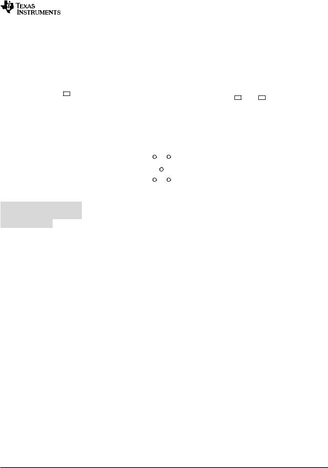
Simplified Schematic |
|
|
Ripple Rejection vs Frequency |
|||||||||
VIN |
|
|
|
VOUT |
|
VOUT |
100 |
|
|
|
|
|
|
VIN |
IN |
|
OUT |
|
|
90 |
|
|
|
|
|
|
|
|
|
TPS730xx |
|
|
|
|
|
|
|
IOUT = 200 MA |
|
||
|
|
|
|
|
|
|
|
|
|
|
|||
0.1μF |
EN |
GND |
NR |
|
2.2μF |
|
80 |
|
|
|
|
|
|
|
(dB) |
|
|
|
|
|
|
|
|||||
|
|
|
0.01μF(1) |
|
|
70 |
|
|
|
|
|
|
|
|
|
|
|
|
|
Rejection |
60 |
|
|
|
|
|
|
|
NOTE: (1) This capacitor is optional. |
|
|
|
50 |
|
|
|
|
|
|
||
|
|
|
Ripple |
|
|
|
|
|
|
|
|||
|
|
|
|
|
|
40 |
IOUT = 10 MA |
|
|
|
|
||
|
|
|
|
|
|
|
|
|
|
|
|
||
|
|
|
|
|
|
|
30 |
|
|
|
|
|
|
|
|
|
|
|
|
|
20 |
VIN = 3.8 V |
|
|
|
|
|
|
|
|
|
|
|
|
|
|
|
|
|
||
|
|
|
|
|
|
|
10 |
COUT = 10 mF |
|
|
|
|
|
|
|
|
|
|
|
|
0 |
CNR = 0.01 mF |
|
|
|
|
|
|
|
|
|
|
|
|
10 |
100 |
1 K |
10 K |
100 K |
1 M |
10 M |
|
|
|
|
|
|
|
|
|
Frequency (Hz) |
|
|
||
An IMPORTANT NOTICE at the end of this data sheet addresses availability, warranty, changes, use in safety-critical applications, intellectual property matters and other important disclaimers. PRODUCTION DATA.

TPS730
SBVS054J –NOVEMBER 2004–REVISED APRIL 2015 www.ti.com
Table of Contents
1 |
Features .................................................................. |
1 |
|
8.1 |
Application Information............................................ |
11 |
|
2 |
Applications ........................................................... |
1 |
|
8.2 |
Typical Application .................................................. |
13 |
|
3 |
Description ............................................................. |
1 |
|
8.3 |
Do's and Don'ts....................................................... |
14 |
|
4 |
Revision History..................................................... |
2 |
9 |
Power Supply Recommendations...................... |
15 |
||
5 |
Pin Configuration and Functions ......................... |
3 |
10 |
Layout................................................................... |
15 |
||
6 |
Specifications |
4 |
|
10.1 |
Layout Guidelines ................................................. |
15 |
|
|
10.2 |
Layout Example |
15 |
||||
|
6.1 |
Absolute Maximum Ratings |
4 |
|
|||
|
|
10.3 |
Thermal Considerations |
16 |
|||
|
6.2 |
ESD Ratings |
4 |
|
|||
|
|
10.4 |
Power Dissipation |
16 |
|||
|
6.3 |
Recommended Operating Conditions |
4 |
|
|||
|
11 Device and Documentation Support |
18 |
|||||
|
6.4 |
Thermal Information .................................................. |
4 |
||||
|
6.5 |
Electrical Characteristics |
5 |
|
11.1 |
Device Support...................................................... |
18 |
|
|
11.2 |
Documentation Support |
18 |
|||
|
6.6 |
Typical Characteristics |
6 |
|
|||
|
|
11.3 |
Trademarks |
18 |
|||
7 |
Detailed Description |
9 |
|
||||
|
11.4 |
Electrostatic Discharge Caution |
18 |
||||
|
7.1 |
Overview |
9 |
|
|||
|
|
11.5 |
Glossary |
18 |
|||
|
7.2 |
Functional Block Diagrams |
9 |
|
|||
|
12 Mechanical, Packaging, and Orderable |
|
|||||
|
7.3 |
Feature Description................................................. |
10 |
18 |
|||
|
7.4 |
Device Functional Modes |
10 |
|
Information ........................................................... |
||
|
|
12.1 TPS730YZQ Nanostar™ Wafer Chip Scale |
|
||||
8 |
Application and Implementation |
11 |
|
|
|||
|
|
Information |
19 |
||||
|
|
|
|
|
|
||
|
|
|
|
|
|
|
|
4 Revision History
NOTE: Page numbers for previous revisions may differ from page numbers in the current version.
Changes from Revision I (February, 2011) to Revision J |
Page |
•Added ESD Ratings table, Feature Description section, Device Functional Modes, Application and Implementation section, Power Supply Recommendations section, Layout section, Device and Documentation Support section, and
Mechanical, Packaging, and Orderable Information section ................................................................................................. |
1 |
• Changed fourth bullet of Features list to low noise ............................................................................................................... |
1 |
• Changed front-page figure ..................................................................................................................................................... |
1 |
• Added Pin Configuration and Functions section .................................................................................................................... |
3 |
• Changed "free-air temperature" to "junction temperature" in Absolute Maximum Ratings condition statement ................... |
4 |
• Deleted Dissipation Ratings table; added Thermal Information table ................................................................................... |
4 |
• Added condition statement to Typical Characteristics ........................................................................................................... |
6 |
• Moved Ordering Information to Device Nomenclature section ............................................................................................ |
18 |
Changes from Revision H (October, 2007) to Revision I |
Page |
• Corrected units in y-axis of Figure 5....................................................................................................................................... |
6 |
2 |
Submit Documentation Feedback |
Copyright © 2004–2015, Texas Instruments Incorporated |
Product Folder Links: TPS730
|
|
|
|
|
|
|
|
|
|
|
|
|
|
|
|
|
|
|
|
|
TPS730 |
www.ti.com |
|
|
|
|
|
|
|
|
|
|
|
|
SBVS054J –NOVEMBER 2004–REVISED APRIL 2015 |
||||||||
5 Pin Configuration and Functions |
|
|
|
|
|
|
|
|
|
||||||||||||
|
|
|
|
DBV Package |
|
|
|
|
DBV Package |
|
|||||||||||
|
|
|
|
5-Pin SOT-23 |
|
|
|
|
|
||||||||||||
|
|
|
|
|
Top View |
|
|
|
|
|
|
6-Pin SOT-23 |
|
||||||||
|
|
|
|
|
|
|
|
|
|
|
|
Top View |
|
||||||||
|
|
|
|
|
|
|
|
|
|
|
|
|
|
|
|
|
|||||
|
|
|
IN |
|
|
1 |
5 |
|
|
OUT |
|
|
|
|
|
|
|
|
|
|
|
|
|
|
|
|
|
|
|
|
|
|
|
|
|
|
|
|
|
||||
|
|
|
|
|
|
|
|
|
|
|
|
|
|
IN |
|
|
1 |
6 |
|
|
OUT |
|
|
GND |
|
2 |
|
|
|
|
|
|
|
|
|
|
|
|
|
|
|
||
|
|
|
|
|
|
|
|
|
|
|
|
|
|
GND |
|
2 |
5 |
|
|
FB |
|
|
|
|
EN |
|
3 |
4 |
|
|
NR |
|
|
|
|
|
|
|
|
|
|
|
|
|
|
|
|
|
|
|
|
|
|
|
|
|
|
|
|
|
|
||||
|
|
|
|
|
|
|
|
|
|
|
|
|
|
EN |
|
|
3 |
4 |
|
|
NR |
|
|
|
Fixed Voltage Versions |
|
|
|
|
|
|
|
|
|
|
|
|||||||
|
|
|
|
|
|
Adjustable Voltage Version |
|||||||||||||||
|
|
|
|
|
|
|
|
|
|
|
|
|
|
||||||||
|
|
|
|
|
|
|
|
|
|
|
YZQ Package |
|
|
|
|
|
|
|
|||
|
|
|
|
|
|
|
|
|
|
|
5-Pin DSBGA |
|
|
|
|
|
|
|
|||
|
|
|
|
|
|
|
|
|
|
|
|
Top View |
|
|
|
|
|
|
|
||
|
|
|
|
|
|
|
|
|
|
|
|
|
|
|
|
|
|
|
|
|
|
|
|
|
|
|
|
|
|
|
|
|
IN |
|
|
OUT |
|
|
|
|
|
|
|
|
|
|
|
|
|
|
|
|
|
|
|
C3 |
C1 |
|
|
|
|
|
|
|
|
|
|
|
|
|
|
|
|
|
|
|
|
|
B2 |
NR |
|
|
|
|
|
|
|
|
|
|
|
|
|
|
|
|
|
|
|
A3 |
A1 |
|
|
|
|
|
|
|
|
|
|
|
|
|
|
|
|
|
|
|
EN |
|
|
GND |
|
|
|
|
|
|
|
|
|
|
|
|
|
|
|
|
|
|
|
|
|
|
|
|
|
|
|
|
|
|
|
|
|
|
|
|
|
|
|
|
Pin Functions |
|
|
|
|
|
|
|
|||
|
|
PIN |
|
|
|
|
|
|
|
|
|
|
|
|
|
|
|
|
|
|
|
NAME |
|
NO. |
|
|
|
|
|
I/O |
|
|
|
DESCRIPTION |
|
|
|
|
|||||
|
SOT-23 |
DSBGA |
|
|
|
|
|
|
|
|
|
|
|
|
|
|
|
||||
|
|
|
|
|
|
|
|
|
|
|
|
|
|
|
|
|
|||||
EN |
|
3 |
|
|
A3 |
|
|
|
I |
Enable pin. Driving the enable pin (EN) high turns on the regulator. Driving this pin low puts |
|||||||||||
|
|
|
|
|
|
the regulator into shutdown mode. EN can be connected to IN if not used. |
|||||||||||||||
|
|
|
|
|
|
|
|
|
|
|
|||||||||||
FB |
|
5 |
|
N/A |
|
|
|
I |
Feedback pin. This terminal is the feedback input pin for the adjustable device. Fixed-voltage |
||||||||||||
|
|
|
|
|
versions in the DBV package do not have this pin. |
|
|
|
|
|
|
|
|||||||||
|
|
|
|
|
|
|
|
|
|
|
|
|
|
|
|
|
|
||||
GND |
|
2 |
|
|
A1 |
|
|
— |
Regulator ground. |
|
|
|
|
|
|
|
|
|
|||
IN |
|
1 |
|
|
C3 |
|
|
|
I |
Input to the device. |
|
|
|
|
|
|
|
|
|
||
OUT |
|
6 |
|
|
C1 |
|
|
O |
Output of the regulator. |
|
|
|
|
|
|
|
|
|
|||
|
|
|
|
|
|
|
|
|
|
|
Noise Reduction pin. Connecting an external capacitor to this pin filters noise generated by |
||||||||||
NR |
|
4 |
|
|
B2 |
|
|
— |
the internal bandgap. This configuration improves power-supply rejection and reduces output |
||||||||||||
|
|
|
|
|
|
|
|
|
|
|
noise. |
|
|
|
|
|
|
|
|
|
|
Copyright © 2004–2015, Texas Instruments Incorporated |
Submit Documentation Feedback |
3 |
Product Folder Links: TPS730

TPS730
SBVS054J –NOVEMBER 2004–REVISED APRIL 2015 |
www.ti.com |
6 Specifications
6.1 Absolute Maximum Ratings
over operating junction temperature range (unless otherwise noted)(1)
|
|
|
MIN |
MAX |
UNIT |
|
|
Input range, VIN |
|
–0.3 |
6 |
|
|
Voltage |
Enable range, VEN |
|
–0.3 |
6 |
V |
|
|
Output range, VOUT |
|
–0.3 |
6 |
|
|
Current |
Peak output, IOUT(max) |
Internally limited |
|
|||
Continuous total power dissipation |
|
See Thermal Information |
|
|||
|
Junction, TJ |
DBV package |
–40 |
150 |
|
|
Temperature |
YZQ package |
–40 |
125 |
°C |
||
|
||||||
|
Storage, Tstg |
|
–65 |
150 |
|
|
(1)Stresses beyond those listed under Absolute Maximum Ratings may cause permanent damage to the device. These are stress ratings only, which do not imply functional operation of the device at these or any other conditions beyond those indicated under Recommended Operating Conditions. Exposure to absolute-maximum-rated conditions for extended periods may affect device reliability.
6.2 |
ESD Ratings |
|
|
|
|
|
|
VALUE |
UNIT |
|
|
Human body model (HBM), per ANSI/ESDA/JEDEC JS-001, all pins(1) |
±2000 |
|
V(ESD) |
Electrostatic discharge |
Charged device model (CDM), per JEDEC specification JESD22-C101, |
±500 |
V |
|
|
all pins(2) |
|
(1)JEDEC document JEP155 states that 500-V HBM allows safe manufacturing with a standard ESD control process.
(2)JEDEC document JEP157 states that 250-V CDM allows safe manufacturing with a standard ESD control process.
6.3 Recommended Operating Conditions
over operating junction temperature range (unless otherwise noted).
|
|
MIN |
NOM |
MAX |
UNIT |
VIN |
Input supply voltage |
2.7 |
|
5.5 |
V |
VEN |
Enable supply voltage |
0 |
|
VIN |
V |
VOUT |
Output voltage |
VFB |
|
5 |
V |
IOUT |
Output current |
0 |
|
200 |
mA |
TJ |
Operating junction temperature |
–40 |
|
125 |
°C |
CIN |
Input capacitor |
0.1 |
1 |
|
µF |
C |
Output capacitor |
2.2(1) |
10 |
|
µF |
OUT |
|
|
|
|
|
CNR |
Noise reduction capacitor |
0 |
10 |
|
nF |
CFF |
Feed-forward capacitor |
|
15 |
|
pF |
R2 |
Lower feedback resistor |
|
30.1 |
|
kΩ |
(1)If CFF is not used or VOUT(nom) < 1.8 V, the minimum recommended COUT = 4.7 µF.
6.4 Thermal Information
|
|
TPS73001 |
|
|
|
THERMAL METRIC(1) |
DBV (SOT-23) |
YZQ (DSBGA) |
UNIT |
|
|
6 PINS |
5 PINS |
|
RθJA |
Junction-to-ambient thermal resistance |
225.1 |
178.5 |
|
RθJC(top) |
Junction-to-case (top) thermal resistance |
78.4 |
1.4 |
|
RθJB |
Junction-to-board thermal resistance |
54.7 |
62.1 |
°C/W |
ψJT |
Junction-to-top characterization parameter |
3.3 |
0.9 |
|
ψJB |
Junction-to-board characterization parameter |
53.8 |
62.1 |
|
(1)For more information about traditional and new thermal metrics, see the IC Package Thermal Metrics application report, SPRA953.
4 |
Submit Documentation Feedback |
Copyright © 2004–2015, Texas Instruments Incorporated |
Product Folder Links: TPS730

TPS730
www.ti.com |
SBVS054J –NOVEMBER 2004–REVISED APRIL 2015 |
6.5 Electrical Characteristics
Over recommended operating temperature range TJ = –40 to +125°C, VEN = VIN, VIN = VOUT(nom) + 1 V(1), IOUT = 1 mA, COUT = 10 μF, CNR = 0.01 μF (unless otherwise noted). Typical values are at 25°C.
|
|
PARAMETER |
|
TEST CONDITIONS |
MIN |
TYP |
|
MAX |
UNIT |
||
V |
|
Input voltage range(1) |
|
|
|
2.7 |
|
5.5 |
V |
||
IN |
|
|
|
|
|
|
|
|
|
|
|
IOUT |
|
Continuous output current |
|
|
|
0 |
|
200 |
mA |
||
VFB |
|
Internal reference (TPS73001) |
|
|
|
1.201 |
1.225 |
1.25 |
V |
||
|
|
Output voltage |
TPS73001 |
|
|
|
VFB |
|
5.5 – VDO |
V |
|
VOUT |
|
range |
|
|
|
|
|||||
|
Output voltage accuracy |
0 µA ≤ IOUT ≤ 200 mA, 2.75 V ≤ VIN ≤ 5.5 V |
–2% |
VOUT(nom) |
2% |
V |
|||||
|
|
||||||||||
V |
VIN) |
Line regulation(1) |
|
V + 1 V ≤ V |
IN |
≤ 5.5 V |
|
0.05 |
|
|
%/V |
OUT( |
|
|
OUT |
|
|
|
|
|
|
||
VOUT( |
IOUT) Load regulation |
|
0 µA ≤ IOUT ≤ 200 mA, TJ = 25°C |
|
5 |
|
|
mV |
|||
VDO |
|
Dropout voltage(2) |
|
IOUT = 200 mA |
|
|
|
120 |
210 |
mV |
|
|
(VIN = VOUT(nom) – 0.1 V) |
|
|
|
|||||||
|
|
|
|
|
|
|
|
|
|
||
ICL |
|
Output current limit |
|
VOUT = 0 V |
|
|
285 |
|
600 |
mA |
|
IGND |
|
Ground pin current |
|
0 µA < IOUT < 200 mA |
|
170 |
250 |
μA |
|||
I |
|
Shutdown current(3) |
|
V = 0 V, 2.7 V ≤ V ≤ 5.5 V |
|
0.07 |
1 |
μA |
|||
SHUTDOWN |
|
|
EN |
|
IN |
|
|
|
|
|
|
IFB |
|
FB pin current |
|
VFB = 1.8 V |
|
|
|
|
1 |
μA |
|
PSRR |
|
Power-supply |
TPS73028 |
f = 100 Hz, IOUT = 200 mA, TJ = 25°C |
|
68 |
|
|
dB |
||
|
rejection ratio |
|
|
|
|||||||
Vn |
|
Output noise |
TPS73018 |
BW = 200 Hz to 100 kHz, IOUT = 200 mA, |
|
33 |
|
|
μVRMS |
||
|
voltage |
CNR = 0.01 μF |
|
|
|
|
|
||||
|
|
|
|
|
|
|
|
|
|
||
tSTR |
|
Start-up time |
TPS73018 |
RL = 14 Ω, COUT = 1 µF, CNR = 0.001 μF |
|
50 |
|
|
μs |
||
VEN(high) |
|
High-level enable input voltage |
2.7 V ≤ VIN ≤ 5.5 V |
1.7 |
|
|
VIN |
V |
|||
VEN(low) |
|
Low-level enable input voltage |
2.7 V ≤ VIN ≤ 5.5 V |
0 |
|
0.7 |
V |
||||
IEN |
|
EN pin current |
|
VEN = 0 V |
|
|
–1 |
|
1 |
μA |
|
|
|
UVLO |
|
Threshold, VCC rising |
2.25 |
|
2.65 |
V |
|||
|
|
|
Hysteresis |
|
|
|
100 |
|
|
mV |
|
|
|
|
|
|
|
|
|
|
|||
(1)Minimum VIN is 2.7 V or VOUT + VDO, whichever is greater.
(2)Dropout is not measured for the TPS73018 and TPS73025 since minimum VIN = 2.7 V.
(3)For adjustable versions, this applies only after VIN is applied; then VEN transitions high to low.
Copyright © 2004–2015, Texas Instruments Incorporated |
Submit Documentation Feedback |
5 |
Product Folder Links: TPS730
TPS730
SBVS054J –NOVEMBER 2004–REVISED APRIL 2015 |
www.ti.com |
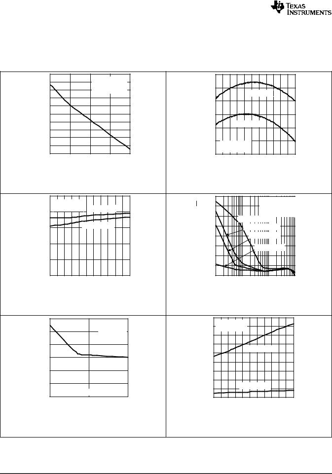
6.6 Typical Characteristics
Over recommended operating temperature range TJ = –40°C to +125°C, VEN = VIN, VIN = VOUT(nom) + 1 V, IOUT = 1 mA, COUT = 10 μF, CNR = 0.01 μF, VOUT(nom) = 2.8 V (unless otherwise noted). Typical values are at TJ = 25°C.
|
2.805 |
|
|
|
|
|
2.805 |
|
|
|
|
|
|
|
|
2.804 |
|
|
VIN = 3.8 V |
|
|
|
|
|
|
|
|
|
|
|
|
|
COUT = 10 mF |
|
|
|
|
|
|
|
|
|
|
|
|
|
|
|
|
|
2.800 |
|
|
|
|
|
|
|
|
|
2.803 |
|
|
TJ = 25°C |
|
|
|
|
|
|
|
|
|
|
|
|
|
|
|
|
|
|
IOUT = 1 MA |
|
|
||||
|
|
|
|
|
|
|
|
|
|
|
|
|||
|
2.802 |
|
|
|
|
|
|
|
|
|
|
|
|
|
|
|
|
|
|
|
|
2.795 |
|
|
|
|
|
|
|
(V) |
2.801 |
|
|
|
|
(V) |
|
|
|
|
|
|
|
|
|
|
|
|
|
|
|
|
|
|
|
|
|
||
OUT |
2.800 |
|
|
|
|
OUT |
2.790 |
|
|
|
|
|
|
|
V |
2.799 |
|
|
|
|
V |
|
IOUT = 200 MA |
|
|
|
|||
|
|
|
|
|
|
|
|
|
|
|||||
|
|
|
|
|
|
|
|
|
|
|
||||
|
2.798 |
|
|
|
|
|
2.785 |
|
|
|
|
|
|
|
|
|
|
|
|
|
|
|
|
|
|
|
|
|
|
|
2.797 |
|
|
|
|
|
|
|
|
|
|
|
|
|
|
|
|
|
|
|
|
2.780 |
VIN = 3.8 V |
|
|
|
|
|
|
|
2.796 |
|
|
|
|
|
|
|
|
|
|
|
|
|
|
|
|
|
|
|
|
|
|
|
|
|
|
|
|
|
|
|
|
|
|
|
|
COUT = 10 mF |
|
|
|
|
|
|
|
2.795 |
|
|
|
|
|
2.775 |
|
|
|
|
|
|
|
|
|
|
|
|
|
|
|
|
|
|
|
|
|
|
|
0 |
50 |
100 |
150 |
200 |
|
|
−40 −25 −10 5 |
20 |
35 |
50 |
65 |
80 |
95 110 125 |
|
|
|
IOUT (mA) |
|
|
|
|
|
TJ (°C) |
|
|
|
||
Figure 1. TPS73028 Output Voltage vs Output Current |
Figure 2. TPS73028 Output Voltage vs Junction |
|
|
|
|
|
|
|
|
|
Temperature |
|
|
|
250 |
|
|
|
|
|
Hz)√V/ |
1.6 |
|
|
|
|
V |
IN |
= 3.8 V |
|
|
|
|
|
VIN = 3.8 V |
|
|
|
COUT = 10 mF |
IOUT = 1 MA |
|
|
1.4 |
|
IOUT = 200 MA |
|
|||
|
|
|
|
|
COUT = 10 mF |
|
|||||
|
200 |
|
|
|
|
|
(m |
|
|
|
|
|
|
|
|
|
|
|
1.2 |
|
|
|
|
A) |
|
|
|
|
|
|
Density |
CNR = 0.001 mF |
|
||
|
|
|
|
|
|
|
|
||||
|
150 |
|
|
|
IOUT = 200 MA |
|
|
1.0 |
CNR = 0.0047 mF |
|
|
|
|
|
|
|
|
|
|
|
|
|
|
(m |
|
|
|
|
|
|
Noise |
0.8 |
|
CNR = 0.01 mF |
|
GND |
|
|
|
|
|
|
|
|
|||
I |
100 |
|
|
|
|
|
Spectral |
0.6 |
|
CNR = 0.1 mF |
|
|
|
|
|
|
|
|
|
|
|
|
|
|
|
|
|
|
|
|
|
0.4 |
|
|
|
|
50 |
|
|
|
|
|
Output |
|
|
|
|
|
|
|
|
|
|
|
0.2 |
|
|
|
|
|
0 |
|
|
|
|
|
|
0 |
|
|
|
|
−40 −25 −10 5 |
20 |
35 50 65 80 |
95 110 125 |
|
100 |
1 K |
10 K |
100 K |
||
|
|
|
|
|
TJ (°C) |
|
|
|
Frequency (Hz) |
|
|
Figure 3. TPS73028 Ground Current vs Junction |
Figure 4. TPS73028 Output Spectral Noise Density vs |
|
|
Temperature |
|
|
|
|
Frequency |
|
|
||||
|
60 |
|
|
|
|
180 |
|
|
|
|
|
|
|
|
|
V |
OUT |
= 2.8 V |
|
|
VIN = 2.7 V |
|
|
|
|
|
|
|
|
|
|
|
160 |
|
|
|
|
|
|
|
|
|
|
IOUT = 200 MA |
|
COUT = 10 mF |
|
|
|
|
|
||||
|
50 |
|
|
|
|
|
|
|
|||||
) |
COUT |
= 10 F |
|
|
|
|
|
|
|
|
|
||
|
|
140 |
|
|
|
|
|
|
|
||||
RMS |
|
|
|
|
|
|
|
|
|
||||
V |
40 |
|
|
|
|
120 |
|
|
|
|
|
|
|
( |
|
|
|
|
|
|
|
|
|
|
|
||
|
|
|
|
|
|
|
|
IOUT = 200 MA |
|
||||
Noise |
|
|
|
|
(mV) |
|
|
|
|
||||
|
|
|
|
100 |
|
|
|
|
|
|
|
||
30 |
|
|
|
|
|
|
|
|
|
|
|
||
Output |
|
|
|
|
DO |
80 |
|
|
|
|
|
|
|
20 |
|
|
|
V |
60 |
|
|
|
|
|
|
|
|
RMS |
10 |
|
|
|
|
40 |
|
|
|
|
|
|
|
|
|
|
|
|
|
|
IOUT = 10 MA |
|
|
||||
|
|
|
|
|
|
|
|
|
|
||||
|
|
|
|
|
|
20 |
|
|
|
|
|
|
|
|
BW = 100 HZ TO 100 KHZ |
|
|
|
|
|
|
|
|
|
|
|
|
|
0 |
|
|
|
|
0 |
|
|
|
|
|
|
|
|
|
|
|
|
|
|
|
|
|
|
|
|
|
|
0.001 |
0.01 |
|
0.1 |
|
−40 −25 −10 5 |
20 |
35 |
50 |
65 |
80 |
95 110 125 |
|
|
|
CNR ( F) |
|
|
|
|
|
|
TJ (°C) |
|
|
|
|
Figure 5. Root Mean Square Output Noise vs CNR |
Figure 6. TPS73028 Dropout Voltage vs Junction |
Temperature
6 |
Submit Documentation Feedback |
Copyright © 2004–2015, Texas Instruments Incorporated |
Product Folder Links: TPS730

TPS730
www.ti.com |
SBVS054J –NOVEMBER 2004–REVISED APRIL 2015 |
Typical Characteristics (continued)
Over recommended operating temperature range TJ = –40°C to +125°C, VEN = VIN, VIN = VOUT(nom) + 1 V, IOUT = 1 mA, COUT = 10 μF, CNR = 0.01 μF, VOUT(nom) = 2.8 V (unless otherwise noted). Typical values are at TJ = 25°C.
|
100 |
|
|
|
|
|
|
|
90 |
|
|
|
IOUT = 200 MA |
|
|
|
|
|
|
|
|
||
|
80 |
|
|
|
|
|
|
(dB) |
70 |
|
|
|
|
|
|
|
|
|
|
|
|
|
|
Rejection |
60 |
|
|
|
|
|
|
50 |
|
|
|
|
|
|
|
|
|
|
|
|
|
|
|
Ripple |
40 |
IOUT = 10 MA |
|
|
|
|
|
|
|
|
|
|
|||
30 |
|
|
|
|
|
|
|
|
|
|
|
|
|
|
|
|
20 |
VIN = 3.8 V |
|
|
|
|
|
|
|
|
|
|
|
||
|
10 |
COUT = 10 mF |
|
|
|
|
|
|
0 |
CNR = 0.01 mF |
|
|
|
|
|
|
10 |
100 |
1 K |
10 K |
100 K |
1 M |
10 M |
Frequency (Hz)
Figure 7. TPS73028 Ripple Rejection vs Frequency
(mV) |
4.8 |
|
|
OUT |
|
V |
3.8 |
|
|
|
IOUT = 200 MA |
|
|
|
|
|
|||
|
|
COUT = 2.2 mF |
|
|
|
|
|
|||
|
20 |
CNR = 0.01 mF |
|
|
DV |
= 0.4 V |
||||
|
|
|
|
|
|
|
DT |
mS |
|
|
(mV) |
|
|
|
|
|
|
|
|
||
0 |
|
|
|
|
|
|
|
|
|
|
IN |
|
|
|
|
|
|
|
|
|
|
V |
|
|
|
|
|
|
|
|
|
|
|
-20 |
|
|
|
|
|
|
|
|
|
|
0 |
10 |
20 |
30 |
40 |
50 |
60 |
70 |
80 |
90 100 |
|
|
|
|
|
Time (ms) |
|
|
|
||
Figure 9. TPS73028 Line Transient Response
VOUT = 3 V |
|
RL = 15 W |
|
mV/div |
|
500 |
|
VIN |
VOUT |
|
|
|
1s/div |
|
4 |
|
|
|
|
|
(V) |
2 |
|
|
|
|
VIN = 3.8 V |
EN |
|
|
|
|
||
|
|
|
|
|
VOUT = 2.8 V |
|
V |
|
|
|
|
|
|
|
0 |
|
|
|
|
IOUT = 200 MA |
|
|
|
|
|
|
|
|
|
|
|
|
|
COUT = 2.2 mF |
|
|
CNR = 0.001 mF |
TJ = 25°C |
|||
|
|
|
||||
|
3 |
|
|
|
|
|
(V) |
2 |
|
|
|
|
|
OUT |
|
|
|
|
|
CNR = 0.0047 mF |
1 |
|
|
|
|
|
|
V |
|
|
|
|
|
|
|
|
|
|
|
CNR = 0.01 mF |
|
|
|
|
|
|
|
|
|
0 |
|
|
|
|
|
|
0 |
20 |
40 |
60 |
80 |
100 120 140 160 180 200 |
|
|
|
|
|
Time (ms) |
|
Figure 8. TPS73028 Output Voltage, Enable Voltage vs Time
|
|
|
|
(Start-Up) |
|
|
|
|
|
|
VIN = 3.8 V |
|
|
|
|
|
20 |
|
COUT |
= 10 mF |
|
|
|
(mV) |
|
|
|
|
|
||
0 |
|
|
|
|
|
|
|
OUT |
−20 |
|
|
|
|
|
|
DV |
|
|
|
|
|
|
|
|
|
|
|
|
|
|
|
|
−40 |
|
|
|
|
|
|
|
300 |
|
|
|
DI |
= |
0.02A |
(mA) |
|
|
|
|
DT |
|
mS |
200 |
|
|
|
|
|
|
|
OUT |
100 |
|
|
|
1MA |
|
|
|
|
|
|
|
|
||
I |
|
|
|
|
|
|
|
|
0 |
0 |
50 100 |
150 200 250 300 |
350 400 450 500 |
||
|
|
|
|
Time (ms) |
|
|
|
Figure 10. TPS73028 Load Transient Response
|
250 |
|
|
|
|
|
|
|
200 |
|
|
|
|
|
|
|
|
|
|
|
|
TJ = 125°C |
|
(mV) |
150 |
|
|
|
|
|
|
|
|
|
TJ = 25°C |
|
|||
DO |
|
|
|
|
|||
|
|
|
|
|
|
|
|
V |
100 |
|
|
|
|
|
|
|
|
|
|
|
|
|
|
|
50 |
|
|
|
|
TJ = −55°C |
|
|
|
|
|
|
|
|
|
|
0 |
|
|
|
|
|
|
|
0 |
20 |
40 |
60 |
80 |
100 120 140 160 180 |
200 |
IOUT (mA)
Figure 11. Power Up and Power Down |
Figure 12. Dropout Voltage vs Output Current |
Copyright © 2004–2015, Texas Instruments Incorporated |
Submit Documentation Feedback |
7 |
Product Folder Links: TPS730
TPS730
SBVS054J –NOVEMBER 2004–REVISED APRIL 2015 |
www.ti.com |
Typical Characteristics (continued)
Over recommended operating temperature range TJ = –40°C to +125°C, VEN = VIN, VIN = VOUT(nom) + 1 V, IOUT = 1 mA, COUT = 10 μF, CNR = 0.01 μF, VOUT(nom) = 2.8 V (unless otherwise noted). Typical values are at TJ = 25°C.
(Ω) |
100 |
COUT = 2.2 F |
|
|
|
|
|
|
|
|
|||
|
VIN = 5.5 V, VOUT ≥ |
1.5 V |
|
|
||
Series Resistance |
|
TJ = −40 °C to 125°C |
|
|
||
10 |
|
|
Region of Instability |
|
||
|
|
|
|
|||
1 |
|
|
|
|
|
|
Equivalent |
|
|
|
|
|
|
0.1 |
|
|
|
|
|
|
|
|
Region of Stability |
|
|
||
ESR, |
|
|
|
|
||
|
|
|
|
|
|
|
|
0.01 |
|
|
|
|
|
|
0 |
0.02 |
0.04 |
0.06 |
0.08 |
0.20 |
IOUT (A)
Figure 13. Typical Regions of Stability Equivalent Series Resistance (ESR) vs Output Current
(Ω) |
100 |
COUT = 10 F |
|
|
|
|
|
|
|
|
|||
|
VIN = 5.5 V |
|
|
|
|
|
Series Resistance |
|
|
|
|
|
|
10 |
TJ = −40 °C to 125°C |
|
|
|||
|
|
|
|
|
||
|
|
|
Region of Instability |
|
||
1 |
|
|
|
|
|
|
Equivalent |
|
|
|
|
|
|
0.1 |
|
Region of Stability |
|
|
||
|
|
|
|
|||
ESR, |
|
|
|
|
||
|
|
|
|
|
|
|
|
0.01 |
|
|
|
|
|
|
0 |
0.02 |
0.04 |
0.06 |
0.08 |
0.20 |
IOUT (A)
Figure 14. Typical Regions of Stability Equivalent Series Resistance (ESR) vs Output Current
8 |
Submit Documentation Feedback |
Copyright © 2004–2015, Texas Instruments Incorporated |
Product Folder Links: TPS730

TPS730
www.ti.com |
SBVS054J –NOVEMBER 2004–REVISED APRIL 2015 |
7 Detailed Description
7.1 Overview
The TPS730 family of low-dropout (LDO) regulators has been optimized for use in noise-sensitive, batteryoperated equipment. The device features extremely low dropout voltages, high PSRR, ultra-low output noise, low quiescent current (170 μA typically), and enable-input to reduce supply currents to less than 1 μA when the regulator is turned off.
7.2 Functional Block Diagrams
IN 
 OUT
OUT
UVLO |
Current |
59 k |
|
||
|
|
|
2.45V |
Sense |
|
|
|
GND |
|
ILIM |
|
SHUTDOWN |
R1 |
|
|
|
|||
|
|
_ |
|
|
|
|
|
|
+ |
FB |
|
|
|
|
|
||
|
|
|
|
|
|
EN |
|
|
|
|
R2 |
|
|
|
|
|
|
|
|
UVLO |
|
|
|
|
Thermal |
|
|
|
|
|
Shutdown |
QuickStart |
|
|
External to |
|
|
|
|
the Device |
|
|
|
|
|
|
|
|
Bandgap |
250 kW |
|
Vref |
|
IN |
Reference |
|
NR |
||
|
|
|
|||
|
1.22V |
|
|
|
|
Figure 15. TPS730 Block Diagram (Adjustable-Voltage Version)
IN |
|
|
|
|
OUT |
|
UVLO |
|
|
|
|
|
2.45V |
Current |
|
|
|
|
|
|
|
|
|
|
|
Sense |
|
|
|
GND |
|
ILIM |
|
SHUTDOWN |
|
|
|
|
|
||
|
|
|
R1 |
|
|
|
|
|
_ |
|
|
|
|
|
+ |
|
|
|
|
|
|
|
|
EN |
|
|
|
|
|
|
|
UVLO |
|
|
|
|
|
|
|
R2 |
|
|
Thermal |
|
|
|
|
|
Shutdown |
|
|
R2 = 40 kW |
|
|
|
QuickStart |
|
|
|
|
|
|
|
|
|
|
Bandgap |
250 kW |
|
Vref |
|
IN |
Reference |
|
NR |
||
|
|
|
|||
|
1.22V |
|
|
|
|
Figure 16. TPS730 Block Diagram (Fixed-Voltage Versions)
Copyright © 2004–2015, Texas Instruments Incorporated |
Submit Documentation Feedback |
9 |
Product Folder Links: TPS730

TPS730
SBVS054J –NOVEMBER 2004–REVISED APRIL 2015 |
www.ti.com |
7.3 Feature Description
7.3.1 Undervoltage Lockout (UVLO)
The TPS730 uses an undervoltage lockout (UVLO) circuit that disables the output until the input voltage is greater than the rising UVLO voltage. This circuit ensures that the device does not exhibit any unpredictable behavior when the supply voltage is lower than the operational range of the internal circuitry, VIN(min).
7.3.2 Shutdown
The enable pin (EN) is active high. Enable the device by forcing the EN pin to exceed VEN(high) (1.7 V, minimum). Turn off the device by forcing the EN pin to drop below 0.7 V. If shutdown capability is not required, connect EN
to IN.
7.3.3 Foldback Current Limit
The TPS730 features internal current limiting and thermal protection. During normal operation, the TPS730 limits output current to approximately 400 mA. When current limiting engages, the output voltage scales back linearly until the overcurrent condition ends. While current limiting is designed to prevent gross device failure, do not exceed the power dissipation ratings of the package or the absolute maximum voltage ratings of the device.
7.4 Device Functional Modes
7.4.1 Normal Operation
The device regulates to the nominal output voltage under the following conditions:
•The input voltage is at least as high as VIN(min).
•The input voltage is greater than the nominal output voltage added to the dropout voltage.
•The enable voltage is greater than VEN(min).
•The output current is less than the current limit.
•The device junction temperature is less than the maximum specified junction temperature.
7.4.2 Dropout Operation
If the input voltage is lower than the nominal output voltage plus the specified dropout voltage, but all other conditions are met for normal operation, the device operates in dropout mode. In this mode of operation, the output voltage is the same as the input voltage minus the dropout voltage. The transient performance of the device is significantly degraded because the pass device is in the linear region and no longer controls the current through the LDO. Line or load transients in dropout can result in large output voltage deviations.
7.4.3 Disabled
The device is disabled under the following conditions:
•The enable voltage is less than the enable falling threshold voltage or has not yet exceeded the enable rising threshold.
•The device junction temperature is greater than the thermal shutdown temperature.
•The input voltage is less than UVLOfalling.
Table 1 shows the conditions that lead to the different modes of operation.
Table 1. Device Functional Mode Comparison
OPERATING MODE |
|
|
|
PARAMETER |
|
|
|
|
VIN |
|
VEN |
|
IOUT |
TJ |
|
|
|
|
|
||||
Normal mode |
VIN > VOUT(nom) + VDO and |
VEN > VEN(high) |
|
IOUT < ILIM |
TJ < 125°C |
||
VIN > VIN(min) |
|
||||||
|
|
|
|
|
|
||
Dropout mode |
VIN(min) < VIN < VOUT(nom) + VDO |
VEN > VEN(high) |
|
— |
TJ < 125°C |
||
Disabled mode |
|
|
|
|
|
|
T > 165°C(1) |
(any true condition disables the |
V |
< UVLO |
V |
< V |
|
— |
|
device) |
IN |
falling |
EN |
EN(low) |
|
|
J |
|
|
|
|
|
|
|
|
(1)Approximate value for thermal shutdown.
10 |
Submit Documentation Feedback |
Copyright © 2004–2015, Texas Instruments Incorporated |
Product Folder Links: TPS730
Loading...