


 Loading...
TMS320C6678
Multicore Fixed and Floating-Point Digital Signal Processor
Data Manual
ADVANCE INFORMATION concerns new products in the sampling or preproduction phase of development. Characteristic data and other specifications are subject to change without notice.
Literature Number: SPRS691
November 2010

TMS320C6678 |
|
|
|
Data Manual |
|
|
|
SPRS691—November 2010 |
|
www.ti.com |
|
|
|
|
|
Release History |
|
|
|
|
|
|
|
|
|
|
|
Release |
Date |
Chapter/Topic |
Description/Comments |
1.0 |
November 2010 |
All |
Initial Release |
|
|
|
|
2 |
Release History |
Copyright 2010 Texas Instruments Incorporated |

TMS320C6678
Multicore Fixed and Floating-Point Digital Signal Processor
www.ti.com |
SPRS691—November 2010 |
|
Contents
1 Features . . . . . . . . . . . . . . . . . . . . . . . . . . . . . . . . . . . . . . . . . . . . . . . . . . . . . . . . . . . . . . . . . . . . . . . . . . . . . . . . . . . . . . . . . . . . . . . . . . . . . . . . .11
1.1 KeyStone Architecture . . . . . . . . . . . . . . . . . . . . . . . . . . . . . . . . . . . . . . . . . . . . . . . . . . . . . . . . . . . . . . . . . . . . . . . . . . . . . . . . . . . . . . . . . . . . . . . . . . . .12 1.2 Device Description . . . . . . . . . . . . . . . . . . . . . . . . . . . . . . . . . . . . . . . . . . . . . . . . . . . . . . . . . . . . . . . . . . . . . . . . . . . . . . . . . . . . . . . . . . . . . . . . . . . . . . .12 1.3 Functional Block Diagram. . . . . . . . . . . . . . . . . . . . . . . . . . . . . . . . . . . . . . . . . . . . . . . . . . . . . . . . . . . . . . . . . . . . . . . . . . . . . . . . . . . . . . . . . . . . . . . . .14
2 Device Overview . . . . . . . . . . . . . . . . . . . . . . . . . . . . . . . . . . . . . . . . . . . . . . . . . . . . . . . . . . . . . . . . . . . . . . . . . . . . . . . . . . . . . . . . . . . . . . . . .15
2.1 Device Characteristics . . . . . . . . . . . . . . . . . . . . . . . . . . . . . . . . . . . . . . . . . . . . . . . . . . . . . . . . . . . . . . . . . . . . . . . . . . . . . . . . . . . . . . . . . . . . . . . . . . . .15 2.2 DSP Core Description . . . . . . . . . . . . . . . . . . . . . . . . . . . . . . . . . . . . . . . . . . . . . . . . . . . . . . . . . . . . . . . . . . . . . . . . . . . . . . . . . . . . . . . . . . . . . . . . . . . . .16 2.3 Memory Map Summary. . . . . . . . . . . . . . . . . . . . . . . . . . . . . . . . . . . . . . . . . . . . . . . . . . . . . . . . . . . . . . . . . . . . . . . . . . . . . . . . . . . . . . . . . . . . . . . . . . .19 2.4 Boot Sequence . . . . . . . . . . . . . . . . . . . . . . . . . . . . . . . . . . . . . . . . . . . . . . . . . . . . . . . . . . . . . . . . . . . . . . . . . . . . . . . . . . . . . . . . . . . . . . . . . . . . . . . . . . .25 2.5 Boot Modes Supported and PLL Settings . . . . . . . . . . . . . . . . . . . . . . . . . . . . . . . . . . . . . . . . . . . . . . . . . . . . . . . . . . . . . . . . . . . . . . . . . . . . . . . . . .26
2.5.1 Boot Device Field . . . . . . . . . . . . . . . . . . . . . . . . . . . . . . . . . . . . . . . . . . . . . . . . . . . . . . . . . . . . . . . . . . . . . . . . . . . . . . . . . . . . . . . . . . . . . . . . . . .26 2.5.2 Device Configuration Field . . . . . . . . . . . . . . . . . . . . . . . . . . . . . . . . . . . . . . . . . . . . . . . . . . . . . . . . . . . . . . . . . . . . . . . . . . . . . . . . . . . . . . . . . .27 2.5.3 PLL Boot Configuration Settings . . . . . . . . . . . . . . . . . . . . . . . . . . . . . . . . . . . . . . . . . . . . . . . . . . . . . . . . . . . . . . . . . . . . . . . . . . . . . . . . . . . . .31 2.6 Second-Level Bootloaders . . . . . . . . . . . . . . . . . . . . . . . . . . . . . . . . . . . . . . . . . . . . . . . . . . . . . . . . . . . . . . . . . . . . . . . . . . . . . . . . . . . . . . . . . . . . . . . .31 2.7 Terminals . . . . . . . . . . . . . . . . . . . . . . . . . . . . . . . . . . . . . . . . . . . . . . . . . . . . . . . . . . . . . . . . . . . . . . . . . . . . . . . . . . . . . . . . . . . . . . . . . . . . . . . . . . . . . . . .32 2.8 Terminal Functions . . . . . . . . . . . . . . . . . . . . . . . . . . . . . . . . . . . . . . . . . . . . . . . . . . . . . . . . . . . . . . . . . . . . . . . . . . . . . . . . . . . . . . . . . . . . . . . . . . . . . . .32 2.9 Development . . . . . . . . . . . . . . . . . . . . . . . . . . . . . . . . . . . . . . . . . . . . . . . . . . . . . . . . . . . . . . . . . . . . . . . . . . . . . . . . . . . . . . . . . . . . . . . . . . . . . . . . . . . .58 2.9.1 Development Support . . . . . . . . . . . . . . . . . . . . . . . . . . . . . . . . . . . . . . . . . . . . . . . . . . . . . . . . . . . . . . . . . . . . . . . . . . . . . . . . . . . . . . . . . . . . . .58 2.9.2 Device Support . . . . . . . . . . . . . . . . . . . . . . . . . . . . . . . . . . . . . . . . . . . . . . . . . . . . . . . . . . . . . . . . . . . . . . . . . . . . . . . . . . . . . . . . . . . . . . . . . . . . .58
3 Device Configuration . . . . . . . . . . . . . . . . . . . . . . . . . . . . . . . . . . . . . . . . . . . . . . . . . . . . . . . . . . . . . . . . . . . . . . . . . . . . . . . . . . . . . . . . . . . . .61
3.1 Device Configuration at Device Reset . . . . . . . . . . . . . . . . . . . . . . . . . . . . . . . . . . . . . . . . . . . . . . . . . . . . . . . . . . . . . . . . . . . . . . . . . . . . . . . . . . . . .61 3.2 Peripheral Selection After Device Reset. . . . . . . . . . . . . . . . . . . . . . . . . . . . . . . . . . . . . . . . . . . . . . . . . . . . . . . . . . . . . . . . . . . . . . . . . . . . . . . . . . . .61 3.3 Device State Control Registers . . . . . . . . . . . . . . . . . . . . . . . . . . . . . . . . . . . . . . . . . . . . . . . . . . . . . . . . . . . . . . . . . . . . . . . . . . . . . . . . . . . . . . . . . . . .62 3.3.1 Device Status Register . . . . . . . . . . . . . . . . . . . . . . . . . . . . . . . . . . . . . . . . . . . . . . . . . . . . . . . . . . . . . . . . . . . . . . . . . . . . . . . . . . . . . . . . . . . . . .64 3.3.2 Device Configuration Register . . . . . . . . . . . . . . . . . . . . . . . . . . . . . . . . . . . . . . . . . . . . . . . . . . . . . . . . . . . . . . . . . . . . . . . . . . . . . . . . . . . . . . .65 3.3.3 JTAG ID (JTAGID) Register Description . . . . . . . . . . . . . . . . . . . . . . . . . . . . . . . . . . . . . . . . . . . . . . . . . . . . . . . . . . . . . . . . . . . . . . . . . . . . . . .65 3.3.4 Kicker Mechanism (KICK0 and KICK1) Register. . . . . . . . . . . . . . . . . . . . . . . . . . . . . . . . . . . . . . . . . . . . . . . . . . . . . . . . . . . . . . . . . . . . . . . .66 3.3.5 LRESETNMI PIN Status (LRSTNMIPINSTAT) Register . . . . . . . . . . . . . . . . . . . . . . . . . . . . . . . . . . . . . . . . . . . . . . . . . . . . . . . . . . . . . . . . . . .66 3.3.6 LRESETNMI PIN Status Clear (LRSTNMIPINSTAT_CLR) Register . . . . . . . . . . . . . . . . . . . . . . . . . . . . . . . . . . . . . . . . . . . . . . . . . . . . . . . .67 3.3.7 Reset Status (RESET_STAT) Register. . . . . . . . . . . . . . . . . . . . . . . . . . . . . . . . . . . . . . . . . . . . . . . . . . . . . . . . . . . . . . . . . . . . . . . . . . . . . . . . . .68 3.3.8 Reset Status Clear (RESET_STAT_CLR) Register . . . . . . . . . . . . . . . . . . . . . . . . . . . . . . . . . . . . . . . . . . . . . . . . . . . . . . . . . . . . . . . . . . . . . . .69 3.3.9 Boot Complete (BOOTCOMPLETE) Register . . . . . . . . . . . . . . . . . . . . . . . . . . . . . . . . . . . . . . . . . . . . . . . . . . . . . . . . . . . . . . . . . . . . . . . . . .70 3.3.10 Power State Control (PWRSTATECTL) Register . . . . . . . . . . . . . . . . . . . . . . . . . . . . . . . . . . . . . . . . . . . . . . . . . . . . . . . . . . . . . . . . . . . . . .71 3.3.11 NMI Even Generation to CorePac (NMIGRx) Register . . . . . . . . . . . . . . . . . . . . . . . . . . . . . . . . . . . . . . . . . . . . . . . . . . . . . . . . . . . . . . . .71 3.3.12 IPC Generation (IPCGRx) Registers . . . . . . . . . . . . . . . . . . . . . . . . . . . . . . . . . . . . . . . . . . . . . . . . . . . . . . . . . . . . . . . . . . . . . . . . . . . . . . . . . .72 3.3.13 IPC Acknowledgement (IPCARx) Registers . . . . . . . . . . . . . . . . . . . . . . . . . . . . . . . . . . . . . . . . . . . . . . . . . . . . . . . . . . . . . . . . . . . . . . . . . .72 3.3.14 IPC Generation Host (IPCGRH) Register . . . . . . . . . . . . . . . . . . . . . . . . . . . . . . . . . . . . . . . . . . . . . . . . . . . . . . . . . . . . . . . . . . . . . . . . . . . . .73 3.3.15 IPC Acknowledgement Host (IPCARH) Register . . . . . . . . . . . . . . . . . . . . . . . . . . . . . . . . . . . . . . . . . . . . . . . . . . . . . . . . . . . . . . . . . . . . .74 3.3.16 Timer Input Selection Register (TINPSEL) . . . . . . . . . . . . . . . . . . . . . . . . . . . . . . . . . . . . . . . . . . . . . . . . . . . . . . . . . . . . . . . . . . . . . . . . . . .75 3.3.17 Timer Output Selection Register (TOUTPSEL) . . . . . . . . . . . . . . . . . . . . . . . . . . . . . . . . . . . . . . . . . . . . . . . . . . . . . . . . . . . . . . . . . . . . . . .77 3.3.18 Reset Mux (RSTMUXx) Register . . . . . . . . . . . . . . . . . . . . . . . . . . . . . . . . . . . . . . . . . . . . . . . . . . . . . . . . . . . . . . . . . . . . . . . . . . . . . . . . . . . . .78 3.4 Pullup/Pulldown Resistors . . . . . . . . . . . . . . . . . . . . . . . . . . . . . . . . . . . . . . . . . . . . . . . . . . . . . . . . . . . . . . . . . . . . . . . . . . . . . . . . . . . . . . . . . . . . . . . .80
4 System Interconnect. . . . . . . . . . . . . . . . . . . . . . . . . . . . . . . . . . . . . . . . . . . . . . . . . . . . . . . . . . . . . . . . . . . . . . . . . . . . . . . . . . . . . . . . . . . . . .81
4.1 Internal Buses, Bridges, and Switch Fabrics . . . . . . . . . . . . . . . . . . . . . . . . . . . . . . . . . . . . . . . . . . . . . . . . . . . . . . . . . . . . . . . . . . . . . . . . . . . . . . . .81 4.2 Data Switch Fabric Connections. . . . . . . . . . . . . . . . . . . . . . . . . . . . . . . . . . . . . . . . . . . . . . . . . . . . . . . . . . . . . . . . . . . . . . . . . . . . . . . . . . . . . . . . . . .82 4.3 Configuration Switch Fabric . . . . . . . . . . . . . . . . . . . . . . . . . . . . . . . . . . . . . . . . . . . . . . . . . . . . . . . . . . . . . . . . . . . . . . . . . . . . . . . . . . . . . . . . . . . . . .84 4.4 Bus Priorities . . . . . . . . . . . . . . . . . . . . . . . . . . . . . . . . . . . . . . . . . . . . . . . . . . . . . . . . . . . . . . . . . . . . . . . . . . . . . . . . . . . . . . . . . . . . . . . . . . . . . . . . . . . . .84
5 C66x CorePac . . . . . . . . . . . . . . . . . . . . . . . . . . . . . . . . . . . . . . . . . . . . . . . . . . . . . . . . . . . . . . . . . . . . . . . . . . . . . . . . . . . . . . . . . . . . . . . . . . . .85
5.1 Memory Architecture . . . . . . . . . . . . . . . . . . . . . . . . . . . . . . . . . . . . . . . . . . . . . . . . . . . . . . . . . . . . . . . . . . . . . . . . . . . . . . . . . . . . . . . . . . . . . . . . . . . . .86 5.1.1 L1P Memory . . . . . . . . . . . . . . . . . . . . . . . . . . . . . . . . . . . . . . . . . . . . . . . . . . . . . . . . . . . . . . . . . . . . . . . . . . . . . . . . . . . . . . . . . . . . . . . . . . . . . . . .86 5.1.2 L1D Memory. . . . . . . . . . . . . . . . . . . . . . . . . . . . . . . . . . . . . . . . . . . . . . . . . . . . . . . . . . . . . . . . . . . . . . . . . . . . . . . . . . . . . . . . . . . . . . . . . . . . . . . .87 5.1.3 L2 Memory . . . . . . . . . . . . . . . . . . . . . . . . . . . . . . . . . . . . . . . . . . . . . . . . . . . . . . . . . . . . . . . . . . . . . . . . . . . . . . . . . . . . . . . . . . . . . . . . . . . . . . . . .87 5.1.4 MSMC SRAM. . . . . . . . . . . . . . . . . . . . . . . . . . . . . . . . . . . . . . . . . . . . . . . . . . . . . . . . . . . . . . . . . . . . . . . . . . . . . . . . . . . . . . . . . . . . . . . . . . . . . . . .88 5.1.5 L3 Memory . . . . . . . . . . . . . . . . . . . . . . . . . . . . . . . . . . . . . . . . . . . . . . . . . . . . . . . . . . . . . . . . . . . . . . . . . . . . . . . . . . . . . . . . . . . . . . . . . . . . . . . . .89
5.2 Memory Protection . . . . . . . . . . . . . . . . . . . . . . . . . . . . . . . . . . . . . . . . . . . . . . . . . . . . . . . . . . . . . . . . . . . . . . . . . . . . . . . . . . . . . . . . . . . . . . . . . . . . . . .89
Copyright 2010 Texas Instruments Incorporated |
Contents |
3 |

TMS320C6678
Multicore Fixed and Floating-Point Digital Signal Processor
SPRS691—November 2010 |
www.ti.com |
|
5.3 Bandwidth Management . . . . . . . . . . . . . . . . . . . . . . . . . . . . . . . . . . . . . . . . . . . . . . . . . . . . . . . . . . . . . . . . . . . . . . . . . . . . . . . . . . . . . . . . . . . . . . . . .90
5.4 Power-Down Control . . . . . . . . . . . . . . . . . . . . . . . . . . . . . . . . . . . . . . . . . . . . . . . . . . . . . . . . . . . . . . . . . . . . . . . . . . . . . . . . . . . . . . . . . . . . . . . . . . . . .90
5.5 C66x CorePac Resets. . . . . . . . . . . . . . . . . . . . . . . . . . . . . . . . . . . . . . . . . . . . . . . . . . . . . . . . . . . . . . . . . . . . . . . . . . . . . . . . . . . . . . . . . . . . . . . . . . . . . .90
5.6 C66x CorePac Revision. . . . . . . . . . . . . . . . . . . . . . . . . . . . . . . . . . . . . . . . . . . . . . . . . . . . . . . . . . . . . . . . . . . . . . . . . . . . . . . . . . . . . . . . . . . . . . . . . . . .91
5.7 C66x CorePac Register Descriptions . . . . . . . . . . . . . . . . . . . . . . . . . . . . . . . . . . . . . . . . . . . . . . . . . . . . . . . . . . . . . . . . . . . . . . . . . . . . . . . . . . . . . . .91
6 Device Operating Conditions . . . . . . . . . . . . . . . . . . . . . . . . . . . . . . . . . . . . . . . . . . . . . . . . . . . . . . . . . . . . . . . . . . . . . . . . . . . . . . . . . . . . .93
6.1 Absolute Maximum Ratings. . . . . . . . . . . . . . . . . . . . . . . . . . . . . . . . . . . . . . . . . . . . . . . . . . . . . . . . . . . . . . . . . . . . . . . . . . . . . . . . . . . . . . . . . . . . . . .93
6.2 Recommended Operating Conditions. . . . . . . . . . . . . . . . . . . . . . . . . . . . . . . . . . . . . . . . . . . . . . . . . . . . . . . . . . . . . . . . . . . . . . . . . . . . . . . . . . . . .94
6.3 Electrical Characteristics . . . . . . . . . . . . . . . . . . . . . . . . . . . . . . . . . . . . . . . . . . . . . . . . . . . . . . . . . . . . . . . . . . . . . . . . . . . . . . . . . . . . . . . . . . . . . . . . . .95
7 TMS320C6678 Peripheral Information and Electrical Specifications. . . . . . . . . . . . . . . . . . . . . . . . . . . . . . . . . . . . . . . . . . . . . . . . .97
7.1 Parameter Information . . . . . . . . . . . . . . . . . . . . . . . . . . . . . . . . . . . . . . . . . . . . . . . . . . . . . . . . . . . . . . . . . . . . . . . . . . . . . . . . . . . . . . . . . . . . . . . . . . .97
7.1.1 1.8-V Signal Transition Levels. . . . . . . . . . . . . . . . . . . . . . . . . . . . . . . . . . . . . . . . . . . . . . . . . . . . . . . . . . . . . . . . . . . . . . . . . . . . . . . . . . . . . . . .97
7.1.2 Timing Parameters and Board Routing Analysis . . . . . . . . . . . . . . . . . . . . . . . . . . . . . . . . . . . . . . . . . . . . . . . . . . . . . . . . . . . . . . . . . . . . . .98
7.2 Recommended Clock and Control Signal Transition Behavior . . . . . . . . . . . . . . . . . . . . . . . . . . . . . . . . . . . . . . . . . . . . . . . . . . . . . . . . . . . . 100
7.3 Power Supplies. . . . . . . . . . . . . . . . . . . . . . . . . . . . . . . . . . . . . . . . . . . . . . . . . . . . . . . . . . . . . . . . . . . . . . . . . . . . . . . . . . . . . . . . . . . . . . . . . . . . . . . . . 100
7.3.1 Power-Supply Sequencing . . . . . . . . . . . . . . . . . . . . . . . . . . . . . . . . . . . . . . . . . . . . . . . . . . . . . . . . . . . . . . . . . . . . . . . . . . . . . . . . . . . . . . . . 100
7.3.2 Power-Down Sequence . . . . . . . . . . . . . . . . . . . . . . . . . . . . . . . . . . . . . . . . . . . . . . . . . . . . . . . . . . . . . . . . . . . . . . . . . . . . . . . . . . . . . . . . . . . 107
7.3.3 Power Supply Decoupling and Bulk Capacitors. . . . . . . . . . . . . . . . . . . . . . . . . . . . . . . . . . . . . . . . . . . . . . . . . . . . . . . . . . . . . . . . . . . . . 108
7.3.4 SmartReflex. . . . . . . . . . . . . . . . . . . . . . . . . . . . . . . . . . . . . . . . . . . . . . . . . . . . . . . . . . . . . . . . . . . . . . . . . . . . . . . . . . . . . . . . . . . . . . . . . . . . . . . 109
7.4 Enhanced Direct Memory Access (EDMA3) Controller . . . . . . . . . . . . . . . . . . . . . . . . . . . . . . . . . . . . . . . . . . . . . . . . . . . . . . . . . . . . . . . . . . . . 112
7.4.1 EDMA3 Device-Specific Information . . . . . . . . . . . . . . . . . . . . . . . . . . . . . . . . . . . . . . . . . . . . . . . . . . . . . . . . . . . . . . . . . . . . . . . . . . . . . . . 113
7.4.2 EDMA3 Channel Synchronization Events. . . . . . . . . . . . . . . . . . . . . . . . . . . . . . . . . . . . . . . . . . . . . . . . . . . . . . . . . . . . . . . . . . . . . . . . . . . 113
7.4.3 EDMA3 Peripheral Register Description(s). . . . . . . . . . . . . . . . . . . . . . . . . . . . . . . . . . . . . . . . . . . . . . . . . . . . . . . . . . . . . . . . . . . . . . . . . . 117
7.5 Interrupts . . . . . . . . . . . . . . . . . . . . . . . . . . . . . . . . . . . . . . . . . . . . . . . . . . . . . . . . . . . . . . . . . . . . . . . . . . . . . . . . . . . . . . . . . . . . . . . . . . . . . . . . . . . . . . 169
7.5.1 Interrupt Sources and Interrupt Controller . . . . . . . . . . . . . . . . . . . . . . . . . . . . . . . . . . . . . . . . . . . . . . . . . . . . . . . . . . . . . . . . . . . . . . . . . 169
7.5.2 INTC Registers . . . . . . . . . . . . . . . . . . . . . . . . . . . . . . . . . . . . . . . . . . . . . . . . . . . . . . . . . . . . . . . . . . . . . . . . . . . . . . . . . . . . . . . . . . . . . . . . . . . . 186
7.5.3 Inter-Processor Register Map . . . . . . . . . . . . . . . . . . . . . . . . . . . . . . . . . . . . . . . . . . . . . . . . . . . . . . . . . . . . . . . . . . . . . . . . . . . . . . . . . . . . . . 192
7.5.4 External Interrupts Electrical Data/Timing. . . . . . . . . . . . . . . . . . . . . . . . . . . . . . . . . . . . . . . . . . . . . . . . . . . . . . . . . . . . . . . . . . . . . . . . . . 193
7.6 MPU . . . . . . . . . . . . . . . . . . . . . . . . . . . . . . . . . . . . . . . . . . . . . . . . . . . . . . . . . . . . . . . . . . . . . . . . . . . . . . . . . . . . . . . . . . . . . . . . . . . . . . . . . . . . . . . . . . . 194
7.6.1 MPU Registers . . . . . . . . . . . . . . . . . . . . . . . . . . . . . . . . . . . . . . . . . . . . . . . . . . . . . . . . . . . . . . . . . . . . . . . . . . . . . . . . . . . . . . . . . . . . . . . . . . . . 195
7.6.2 MPU Programmable Range Registers . . . . . . . . . . . . . . . . . . . . . . . . . . . . . . . . . . . . . . . . . . . . . . . . . . . . . . . . . . . . . . . . . . . . . . . . . . . . . . 199
7.7 Reset Controller . . . . . . . . . . . . . . . . . . . . . . . . . . . . . . . . . . . . . . . . . . . . . . . . . . . . . . . . . . . . . . . . . . . . . . . . . . . . . . . . . . . . . . . . . . . . . . . . . . . . . . . . 208
7.7.1 Power-on Reset . . . . . . . . . . . . . . . . . . . . . . . . . . . . . . . . . . . . . . . . . . . . . . . . . . . . . . . . . . . . . . . . . . . . . . . . . . . . . . . . . . . . . . . . . . . . . . . . . . . 208
7.7.2 Hard Reset. . . . . . . . . . . . . . . . . . . . . . . . . . . . . . . . . . . . . . . . . . . . . . . . . . . . . . . . . . . . . . . . . . . . . . . . . . . . . . . . . . . . . . . . . . . . . . . . . . . . . . . . 209
7.7.3 Soft Reset. . . . . . . . . . . . . . . . . . . . . . . . . . . . . . . . . . . . . . . . . . . . . . . . . . . . . . . . . . . . . . . . . . . . . . . . . . . . . . . . . . . . . . . . . . . . . . . . . . . . . . . . . 210
7.7.4 Local Reset . . . . . . . . . . . . . . . . . . . . . . . . . . . . . . . . . . . . . . . . . . . . . . . . . . . . . . . . . . . . . . . . . . . . . . . . . . . . . . . . . . . . . . . . . . . . . . . . . . . . . . . 211
7.7.5 Reset Priority . . . . . . . . . . . . . . . . . . . . . . . . . . . . . . . . . . . . . . . . . . . . . . . . . . . . . . . . . . . . . . . . . . . . . . . . . . . . . . . . . . . . . . . . . . . . . . . . . . . . . 211
7.7.6 Reset Controller Register . . . . . . . . . . . . . . . . . . . . . . . . . . . . . . . . . . . . . . . . . . . . . . . . . . . . . . . . . . . . . . . . . . . . . . . . . . . . . . . . . . . . . . . . . . 211
7.7.7 Reset Electrical Data / Timing. . . . . . . . . . . . . . . . . . . . . . . . . . . . . . . . . . . . . . . . . . . . . . . . . . . . . . . . . . . . . . . . . . . . . . . . . . . . . . . . . . . . . . 211
7.8 Main PLL and PLL Controller . . . . . . . . . . . . . . . . . . . . . . . . . . . . . . . . . . . . . . . . . . . . . . . . . . . . . . . . . . . . . . . . . . . . . . . . . . . . . . . . . . . . . . . . . . . . 215
7.8.1 Main PLL Controller Device-Specific Information . . . . . . . . . . . . . . . . . . . . . . . . . . . . . . . . . . . . . . . . . . . . . . . . . . . . . . . . . . . . . . . . . . . 216
7.8.2 PLL Controller Memory Map. . . . . . . . . . . . . . . . . . . . . . . . . . . . . . . . . . . . . . . . . . . . . . . . . . . . . . . . . . . . . . . . . . . . . . . . . . . . . . . . . . . . . . . 217
7.8.3 Main PLL Control Register . . . . . . . . . . . . . . . . . . . . . . . . . . . . . . . . . . . . . . . . . . . . . . . . . . . . . . . . . . . . . . . . . . . . . . . . . . . . . . . . . . . . . . . . . 224
7.8.4 Main PLL Controller/SRIO/HyperLink/PCIe Clock Input Electrical Data/Timing . . . . . . . . . . . . . . . . . . . . . . . . . . . . . . . . . . . . . . . 224
7.9 DD3 PLL. . . . . . . . . . . . . . . . . . . . . . . . . . . . . . . . . . . . . . . . . . . . . . . . . . . . . . . . . . . . . . . . . . . . . . . . . . . . . . . . . . . . . . . . . . . . . . . . . . . . . . . . . . . . . . . . 228
7.9.1 DDR3 PLL Control Register . . . . . . . . . . . . . . . . . . . . . . . . . . . . . . . . . . . . . . . . . . . . . . . . . . . . . . . . . . . . . . . . . . . . . . . . . . . . . . . . . . . . . . . . 228
7.9.2 DDR3 PLL Device-Specific Information. . . . . . . . . . . . . . . . . . . . . . . . . . . . . . . . . . . . . . . . . . . . . . . . . . . . . . . . . . . . . . . . . . . . . . . . . . . . . 229
7.9.3 DDR3 PLL Input Clock Electrical Data/Timing. . . . . . . . . . . . . . . . . . . . . . . . . . . . . . . . . . . . . . . . . . . . . . . . . . . . . . . . . . . . . . . . . . . . . . . 229
7.10 PASS PLL. . . . . . . . . . . . . . . . . . . . . . . . . . . . . . . . . . . . . . . . . . . . . . . . . . . . . . . . . . . . . . . . . . . . . . . . . . . . . . . . . . . . . . . . . . . . . . . . . . . . . . . . . . . . . . 230
7.10.1 PASS PLL Control Register. . . . . . . . . . . . . . . . . . . . . . . . . . . . . . . . . . . . . . . . . . . . . . . . . . . . . . . . . . . . . . . . . . . . . . . . . . . . . . . . . . . . . . . . 230
7.10.2 PASS PLL Device-Specific Information . . . . . . . . . . . . . . . . . . . . . . . . . . . . . . . . . . . . . . . . . . . . . . . . . . . . . . . . . . . . . . . . . . . . . . . . . . . . 231
7.11 DDR3 Memory Controller. . . . . . . . . . . . . . . . . . . . . . . . . . . . . . . . . . . . . . . . . . . . . . . . . . . . . . . . . . . . . . . . . . . . . . . . . . . . . . . . . . . . . . . . . . . . . . 232
7.11.1 DDR3 Memory Controller Device-Specific Information . . . . . . . . . . . . . . . . . . . . . . . . . . . . . . . . . . . . . . . . . . . . . . . . . . . . . . . . . . . . 232
7.11.2 DDR3 Memory Controller Electrical Data/Timing . . . . . . . . . . . . . . . . . . . . . . . . . . . . . . . . . . . . . . . . . . . . . . . . . . . . . . . . . . . . . . . . . . 233
7.12 I2C Peripheral . . . . . . . . . . . . . . . . . . . . . . . . . . . . . . . . . . . . . . . . . . . . . . . . . . . . . . . . . . . . . . . . . . . . . . . . . . . . . . . . . . . . . . . . . . . . . . . . . . . . . . . . . 233
7.12.1 I2C Device-Specific Information . . . . . . . . . . . . . . . . . . . . . . . . . . . . . . . . . . . . . . . . . . . . . . . . . . . . . . . . . . . . . . . . . . . . . . . . . . . . . . . . . . 233
7.12.2 I2C Peripheral Register Description(s). . . . . . . . . . . . . . . . . . . . . . . . . . . . . . . . . . . . . . . . . . . . . . . . . . . . . . . . . . . . . . . . . . . . . . . . . . . . . 234
7.12.3 I2C Electrical Data/Timing . . . . . . . . . . . . . . . . . . . . . . . . . . . . . . . . . . . . . . . . . . . . . . . . . . . . . . . . . . . . . . . . . . . . . . . . . . . . . . . . . . . . . . . . 235
4 |
Contents |
Copyright 2010 Texas Instruments Incorporated |

TMS320C6678
Multicore Fixed and Floating-Point Digital Signal Processor
www.ti.com |
SPRS691—November 2010 |
|
7.13 SPI Peripheral . . . . . . . . . . . . . . . . . . . . . . . . . . . . . . . . . . . . . . . . . . . . . . . . . . . . . . . . . . . . . . . . . . . . . . . . . . . . . . . . . . . . . . . . . . . . . . . . . . . . . . . . . 238
7.13.1 SPI Electrical Data/Timing . . . . . . . . . . . . . . . . . . . . . . . . . . . . . . . . . . . . . . . . . . . . . . . . . . . . . . . . . . . . . . . . . . . . . . . . . . . . . . . . . . . . . . . . 238
7.14 HyperLink Peripheral . . . . . . . . . . . . . . . . . . . . . . . . . . . . . . . . . . . . . . . . . . . . . . . . . . . . . . . . . . . . . . . . . . . . . . . . . . . . . . . . . . . . . . . . . . . . . . . . . . 241
7.15 UART Peripheral. . . . . . . . . . . . . . . . . . . . . . . . . . . . . . . . . . . . . . . . . . . . . . . . . . . . . . . . . . . . . . . . . . . . . . . . . . . . . . . . . . . . . . . . . . . . . . . . . . . . . . . 243
7.16 PCIe Peripheral. . . . . . . . . . . . . . . . . . . . . . . . . . . . . . . . . . . . . . . . . . . . . . . . . . . . . . . . . . . . . . . . . . . . . . . . . . . . . . . . . . . . . . . . . . . . . . . . . . . . . . . . 244
7.17 TSIP Peripheral . . . . . . . . . . . . . . . . . . . . . . . . . . . . . . . . . . . . . . . . . . . . . . . . . . . . . . . . . . . . . . . . . . . . . . . . . . . . . . . . . . . . . . . . . . . . . . . . . . . . . . . . 244
7.18 EMIF16 Peripheral . . . . . . . . . . . . . . . . . . . . . . . . . . . . . . . . . . . . . . . . . . . . . . . . . . . . . . . . . . . . . . . . . . . . . . . . . . . . . . . . . . . . . . . . . . . . . . . . . . . . . 244
7.19 Packet Accelerator . . . . . . . . . . . . . . . . . . . . . . . . . . . . . . . . . . . . . . . . . . . . . . . . . . . . . . . . . . . . . . . . . . . . . . . . . . . . . . . . . . . . . . . . . . . . . . . . . . . . 245
7.20 Security Accelerator . . . . . . . . . . . . . . . . . . . . . . . . . . . . . . . . . . . . . . . . . . . . . . . . . . . . . . . . . . . . . . . . . . . . . . . . . . . . . . . . . . . . . . . . . . . . . . . . . . . 245
7.21 Ethernet MAC (EMAC) . . . . . . . . . . . . . . . . . . . . . . . . . . . . . . . . . . . . . . . . . . . . . . . . . . . . . . . . . . . . . . . . . . . . . . . . . . . . . . . . . . . . . . . . . . . . . . . . . 246
7.22 Management Data Input/Output (MDIO). . . . . . . . . . . . . . . . . . . . . . . . . . . . . . . . . . . . . . . . . . . . . . . . . . . . . . . . . . . . . . . . . . . . . . . . . . . . . . . 247
7.23 Timers . . . . . . . . . . . . . . . . . . . . . . . . . . . . . . . . . . . . . . . . . . . . . . . . . . . . . . . . . . . . . . . . . . . . . . . . . . . . . . . . . . . . . . . . . . . . . . . . . . . . . . . . . . . . . . . . 248
7.23.1 Timers Device-Specific Information. . . . . . . . . . . . . . . . . . . . . . . . . . . . . . . . . . . . . . . . . . . . . . . . . . . . . . . . . . . . . . . . . . . . . . . . . . . . . . . 248
7.23.2 Timers Electrical Data/Timing . . . . . . . . . . . . . . . . . . . . . . . . . . . . . . . . . . . . . . . . . . . . . . . . . . . . . . . . . . . . . . . . . . . . . . . . . . . . . . . . . . . . 248
7.24 Serial RapidIO (SRIO) Port. . . . . . . . . . . . . . . . . . . . . . . . . . . . . . . . . . . . . . . . . . . . . . . . . . . . . . . . . . . . . . . . . . . . . . . . . . . . . . . . . . . . . . . . . . . . . . 249
7.25 General-Purpose Input/Output (GPIO) . . . . . . . . . . . . . . . . . . . . . . . . . . . . . . . . . . . . . . . . . . . . . . . . . . . . . . . . . . . . . . . . . . . . . . . . . . . . . . . . . 250
7.25.1 GPIO Device-Specific Information . . . . . . . . . . . . . . . . . . . . . . . . . . . . . . . . . . . . . . . . . . . . . . . . . . . . . . . . . . . . . . . . . . . . . . . . . . . . . . . . 250
7.25.2 GPIO Electrical Data/Timing . . . . . . . . . . . . . . . . . . . . . . . . . . . . . . . . . . . . . . . . . . . . . . . . . . . . . . . . . . . . . . . . . . . . . . . . . . . . . . . . . . . . . . 250
7.26 Semaphore2 . . . . . . . . . . . . . . . . . . . . . . . . . . . . . . . . . . . . . . . . . . . . . . . . . . . . . . . . . . . . . . . . . . . . . . . . . . . . . . . . . . . . . . . . . . . . . . . . . . . . . . . . . . 250
7.27 Emulation Features and Capability. . . . . . . . . . . . . . . . . . . . . . . . . . . . . . . . . . . . . . . . . . . . . . . . . . . . . . . . . . . . . . . . . . . . . . . . . . . . . . . . . . . . . 251
7.27.1 Advanced Event Triggering (AET) . . . . . . . . . . . . . . . . . . . . . . . . . . . . . . . . . . . . . . . . . . . . . . . . . . . . . . . . . . . . . . . . . . . . . . . . . . . . . . . . 251
7.27.2 Trace . . . . . . . . . . . . . . . . . . . . . . . . . . . . . . . . . . . . . . . . . . . . . . . . . . . . . . . . . . . . . . . . . . . . . . . . . . . . . . . . . . . . . . . . . . . . . . . . . . . . . . . . . . . . 251
7.27.3 IEEE 1149.1 JTAG . . . . . . . . . . . . . . . . . . . . . . . . . . . . . . . . . . . . . . . . . . . . . . . . . . . . . . . . . . . . . . . . . . . . . . . . . . . . . . . . . . . . . . . . . . . . . . . . 252
8 Mechanical Data . . . . . . . . . . . . . . . . . . . . . . . . . . . . . . . . . . . . . . . . . . . . . . . . . . . . . . . . . . . . . . . . . . . . . . . . . . . . . . . . . . . . . . . . . . . . . . . 255
8.1 Thermal Data. . . . . . . . . . . . . . . . . . . . . . . . . . . . . . . . . . . . . . . . . . . . . . . . . . . . . . . . . . . . . . . . . . . . . . . . . . . . . . . . . . . . . . . . . . . . . . . . . . . . . . . . . . . 255
8.2 Packaging Information . . . . . . . . . . . . . . . . . . . . . . . . . . . . . . . . . . . . . . . . . . . . . . . . . . . . . . . . . . . . . . . . . . . . . . . . . . . . . . . . . . . . . . . . . . . . . . . . . 255
8.3 Package CYP . . . . . . . . . . . . . . . . . . . . . . . . . . . . . . . . . . . . . . . . . . . . . . . . . . . . . . . . . . . . . . . . . . . . . . . . . . . . . . . . . . . . . . . . . . . . . . . . . . . . . . . . . . . 256
Copyright 2010 Texas Instruments Incorporated |
Contents |
5 |

TMS320C6678
Multicore Fixed and Floating-Point Digital Signal Processor
SPRS691—November 2010 |
www.ti.com |
|
List of Figures
Figure 1-1 Functional Block Diagram . . . . . . . . . . . . . . . . . . . . . . . . . . . . . . . . . . . . . . . . . . . . . . . . . . . . . . . . . . . . . . . . . . . . . . . . . . . . . . . . . . . . . . . .14 Figure 2-1 TMS320C6678 DSP Core Data Paths . . . . . . . . . . . . . . . . . . . . . . . . . . . . . . . . . . . . . . . . . . . . . . . . . . . . . . . . . . . . . . . . . . . . . . . . . . . . . . .18 Figure 2-2 Boot Mode Pin Decoding . . . . . . . . . . . . . . . . . . . . . . . . . . . . . . . . . . . . . . . . . . . . . . . . . . . . . . . . . . . . . . . . . . . . . . . . . . . . . . . . . . . . . . . . .26 Figure 2-3 Sleep / EMIF16 Configuration Bit Fields. . . . . . . . . . . . . . . . . . . . . . . . . . . . . . . . . . . . . . . . . . . . . . . . . . . . . . . . . . . . . . . . . . . . . . . . . . . .27 Figure 2-4 Ethernet (SGMII) Device Configuration Bit Fields. . . . . . . . . . . . . . . . . . . . . . . . . . . . . . . . . . . . . . . . . . . . . . . . . . . . . . . . . . . . . . . . . . .27 Figure 2-5 Serial Rapid I/O Device Configuration Bit Fields. . . . . . . . . . . . . . . . . . . . . . . . . . . . . . . . . . . . . . . . . . . . . . . . . . . . . . . . . . . . . . . . . . . .28
Figure 2-6 PCI Device Configuration Bit Fields. . . . . . . . . . . . . . . . . . . . . . . . . . . . . . . . . . . . . . . . . . . . . . . . . . . . . . . . . . . . . . . . . . . . . . . . . . . . . . . .28 Figure 2-7 I2C Master Mode Device Configuration Bit Fields . . . . . . . . . . . . . . . . . . . . . . . . . . . . . . . . . . . . . . . . . . . . . . . . . . . . . . . . . . . . . . . . . .29 Figure 2-8 I2C Passive Mode Device Configuration Bit Fields . . . . . . . . . . . . . . . . . . . . . . . . . . . . . . . . . . . . . . . . . . . . . . . . . . . . . . . . . . . . . . . . . .30
Figure 2-9 SPI Device Configuration Bit Fields . . . . . . . . . . . . . . . . . . . . . . . . . . . . . . . . . . . . . . . . . . . . . . . . . . . . . . . . . . . . . . . . . . . . . . . . . . . . . . . .30 Figure 2-10 HyperLink Boot Device Configuration Fields. . . . . . . . . . . . . . . . . . . . . . . . . . . . . . . . . . . . . . . . . . . . . . . . . . . . . . . . . . . . . . . . . . . . . . .31 Figure 2-11 CYP 841-Pin BGA Package Bottom View . . . . . . . . . . . . . . . . . . . . . . . . . . . . . . . . . . . . . . . . . . . . . . . . . . . . . . . . . . . . . . . . . . . . . . . . . . .32 Figure 3-1 Device Status Register . . . . . . . . . . . . . . . . . . . . . . . . . . . . . . . . . . . . . . . . . . . . . . . . . . . . . . . . . . . . . . . . . . . . . . . . . . . . . . . . . . . . . . . . . . . .64 Figure 3-2 Device Configuration Register (DEVCFG) . . . . . . . . . . . . . . . . . . . . . . . . . . . . . . . . . . . . . . . . . . . . . . . . . . . . . . . . . . . . . . . . . . . . . . . . . .65 Figure 3-3 JTAG ID (JTAGID) Register. . . . . . . . . . . . . . . . . . . . . . . . . . . . . . . . . . . . . . . . . . . . . . . . . . . . . . . . . . . . . . . . . . . . . . . . . . . . . . . . . . . . . . . . .65 Figure 3-4 LRESETNMI PIN Status Register (LRSTNMIPINSTAT) . . . . . . . . . . . . . . . . . . . . . . . . . . . . . . . . . . . . . . . . . . . . . . . . . . . . . . . . . . . . . . . .66 Figure 3-5 LRESETNMI PIN Status Clear Register (LRSTNMIPINSTAT_CLR) . . . . . . . . . . . . . . . . . . . . . . . . . . . . . . . . . . . . . . . . . . . . . . . . . . . . . .67 Figure 3-6 Reset Status Register (RESET_STAT) . . . . . . . . . . . . . . . . . . . . . . . . . . . . . . . . . . . . . . . . . . . . . . . . . . . . . . . . . . . . . . . . . . . . . . . . . . . . . . .68 Figure 3-7 Reset Status Clear Register (RESET_STAT_CLR). . . . . . . . . . . . . . . . . . . . . . . . . . . . . . . . . . . . . . . . . . . . . . . . . . . . . . . . . . . . . . . . . . . . .69 Figure 3-8 Boot Complete Register (BOOTCOMPLETE) . . . . . . . . . . . . . . . . . . . . . . . . . . . . . . . . . . . . . . . . . . . . . . . . . . . . . . . . . . . . . . . . . . . . . . . .70 Figure 3-9 Power State Control Register (PWRSTATECTL) . . . . . . . . . . . . . . . . . . . . . . . . . . . . . . . . . . . . . . . . . . . . . . . . . . . . . . . . . . . . . . . . . . . . .71 Figure 3-10 NMI Generation Register (NMIGRx) . . . . . . . . . . . . . . . . . . . . . . . . . . . . . . . . . . . . . . . . . . . . . . . . . . . . . . . . . . . . . . . . . . . . . . . . . . . . . . . .71 Figure 3-11 IPC Generation Registers (IPCGRx) . . . . . . . . . . . . . . . . . . . . . . . . . . . . . . . . . . . . . . . . . . . . . . . . . . . . . . . . . . . . . . . . . . . . . . . . . . . . . . . .72 Figure 3-12 IPC Acknowledgement Registers (IPCARx) . . . . . . . . . . . . . . . . . . . . . . . . . . . . . . . . . . . . . . . . . . . . . . . . . . . . . . . . . . . . . . . . . . . . . . . . .73 Figure 3-13 IPC Generation Registers (IPCGRH) . . . . . . . . . . . . . . . . . . . . . . . . . . . . . . . . . . . . . . . . . . . . . . . . . . . . . . . . . . . . . . . . . . . . . . . . . . . . . . . .73 Figure 3-14 IPC Acknowledgement Register (IPCARH) . . . . . . . . . . . . . . . . . . . . . . . . . . . . . . . . . . . . . . . . . . . . . . . . . . . . . . . . . . . . . . . . . . . . . . . . .74 Figure 3-15 Timer Input Selection Register (TINPSEL) . . . . . . . . . . . . . . . . . . . . . . . . . . . . . . . . . . . . . . . . . . . . . . . . . . . . . . . . . . . . . . . . . . . . . . . . . .75 Figure 3-16 Timer Output Selection Register (TOUTPSEL) . . . . . . . . . . . . . . . . . . . . . . . . . . . . . . . . . . . . . . . . . . . . . . . . . . . . . . . . . . . . . . . . . . . . . .77 Figure 3-17 Reset Mux Register RSTMUXx . . . . . . . . . . . . . . . . . . . . . . . . . . . . . . . . . . . . . . . . . . . . . . . . . . . . . . . . . . . . . . . . . . . . . . . . . . . . . . . . . . . . .78 Figure 4-1 Packed DMA Priority Allocation Register (PKTDMA_PRI_ALLOC). . . . . . . . . . . . . . . . . . . . . . . . . . . . . . . . . . . . . . . . . . . . . . . . . . . .84 Figure 5-1 C66x CorePac Block Diagram . . . . . . . . . . . . . . . . . . . . . . . . . . . . . . . . . . . . . . . . . . . . . . . . . . . . . . . . . . . . . . . . . . . . . . . . . . . . . . . . . . . . .85 Figure 5-2 TMS320C6678 L1P Memory Configurations . . . . . . . . . . . . . . . . . . . . . . . . . . . . . . . . . . . . . . . . . . . . . . . . . . . . . . . . . . . . . . . . . . . . . . .86 Figure 5-3 TMS320C6678 L1D Memory Configurations . . . . . . . . . . . . . . . . . . . . . . . . . . . . . . . . . . . . . . . . . . . . . . . . . . . . . . . . . . . . . . . . . . . . . . .87 Figure 5-4 TMS320C6678 L2 Memory Configurations. . . . . . . . . . . . . . . . . . . . . . . . . . . . . . . . . . . . . . . . . . . . . . . . . . . . . . . . . . . . . . . . . . . . . . . . .88 Figure 7-1 Test Load Circuit for AC Timing Measurements . . . . . . . . . . . . . . . . . . . . . . . . . . . . . . . . . . . . . . . . . . . . . . . . . . . . . . . . . . . . . . . . . . . .97 Figure 7-2 Input and Output Voltage Reference Levels for AC Timing Measurements . . . . . . . . . . . . . . . . . . . . . . . . . . . . . . . . . . . . . . . . . .97 Figure 7-3 Rise and Fall Transition Time Voltage Reference Levels. . . . . . . . . . . . . . . . . . . . . . . . . . . . . . . . . . . . . . . . . . . . . . . . . . . . . . . . . . . . .98 Figure 7-4 Board-Level Input/Output Timings . . . . . . . . . . . . . . . . . . . . . . . . . . . . . . . . . . . . . . . . . . . . . . . . . . . . . . . . . . . . . . . . . . . . . . . . . . . . . . . .99 Figure 7-5 POR-Controlled Power Sequencing — Core Before IO. . . . . . . . . . . . . . . . . . . . . . . . . . . . . . . . . . . . . . . . . . . . . . . . . . . . . . . . . . . . .102 Figure 7-6 POR-Controlled Power Sequencing — IO Before Core. . . . . . . . . . . . . . . . . . . . . . . . . . . . . . . . . . . . . . . . . . . . . . . . . . . . . . . . . . . . .103 Figure 7-7 RESETFULL-Controlled Device Initialization — Core Before IO . . . . . . . . . . . . . . . . . . . . . . . . . . . . . . . . . . . . . . . . . . . . . . . . . . . . .105 Figure 7-8 RESETFULL-Controlled Device Initialization — IO Before Core . . . . . . . . . . . . . . . . . . . . . . . . . . . . . . . . . . . . . . . . . . . . . . . . . . . . .106
Figure 7-9 SmartReflex 4-Pin VID Interface Timing. . . . . . . . . . . . . . . . . . . . . . . . . . . . . . . . . . . . . . . . . . . . . . . . . . . . . . . . . . . . . . . . . . . . . . . . . . .109 Figure 7-10 SmartReflex I2C Interface Receive Timings. . . . . . . . . . . . . . . . . . . . . . . . . . . . . . . . . . . . . . . . . . . . . . . . . . . . . . . . . . . . . . . . . . . . . . . .110 Figure 7-11 SmartReflex I2C Interface Transmit Timings. . . . . . . . . . . . . . . . . . . . . . . . . . . . . . . . . . . . . . . . . . . . . . . . . . . . . . . . . . . . . . . . . . . . . . .111
Figure 7-12 TMS320C6678 Interrupt Topology . . . . . . . . . . . . . . . . . . . . . . . . . . . . . . . . . . . . . . . . . . . . . . . . . . . . . . . . . . . . . . . . . . . . . . . . . . . . . . .170 Figure 7-13 NMI and Local Reset Timing . . . . . . . . . . . . . . . . . . . . . . . . . . . . . . . . . . . . . . . . . . . . . . . . . . . . . . . . . . . . . . . . . . . . . . . . . . . . . . . . . . . . .193 Figure 7-14 Configuration Register (CONFIG) . . . . . . . . . . . . . . . . . . . . . . . . . . . . . . . . . . . . . . . . . . . . . . . . . . . . . . . . . . . . . . . . . . . . . . . . . . . . . . . . .199 Figure 7-15 Programmable Range n Start Address Register (PROGn_MPSAR) . . . . . . . . . . . . . . . . . . . . . . . . . . . . . . . . . . . . . . . . . . . . . . . . . .200 Figure 7-16 Programmable Range n End Address Register (PROGn_MPEAR). . . . . . . . . . . . . . . . . . . . . . . . . . . . . . . . . . . . . . . . . . . . . . . . . . .202 Figure 7-17 Programmable Range n Memory Protection Page Attribute Register (PROGn_MPPA) . . . . . . . . . . . . . . . . . . . . . . . . . . . . . .205
6 |
List of Figures |
Copyright 2010 Texas Instruments Incorporated |

TMS320C6678
Multicore Fixed and Floating-Point Digital Signal Processor
|
|
SPRS691—November 2010 |
www.ti.com |
|
|
Figure 7-18 |
Power-On Reset Timing. . . . . . . . . . . . . . . . . . . . . . . . . . . . . . . . . . . . . . . . . . . . . . . . . . . . . . . . . . . . . . . . . . . . |
. . . . . . . . . . . . . . . . . . . . . .212 |
Figure 7-19 |
Full-Reset Timing. . . . . . . . . . . . . . . . . . . . . . . . . . . . . . . . . . . . . . . . . . . . . . . . . . . . . . . . . . . . . . . . . . . . . . . . . . |
. . . . . . . . . . . . . . . . . . . . . .212 |
Figure 7-20 |
Hard-Reset Timing. . . . . . . . . . . . . . . . . . . . . . . . . . . . . . . . . . . . . . . . . . . . . . . . . . . . . . . . . . . . . . . . . . . . . . . . . |
. . . . . . . . . . . . . . . . . . . . . .213 |
Figure 7-21 |
Soft-Reset Timing . . . . . . . . . . . . . . . . . . . . . . . . . . . . . . . . . . . . . . . . . . . . . . . . . . . . . . . . . . . . . . . . . . . . . . . . . |
. . . . . . . . . . . . . . . . . . . . . .213 |
Figure 7-22 |
Boot Configuration Timing . . . . . . . . . . . . . . . . . . . . . . . . . . . . . . . . . . . . . . . . . . . . . . . . . . . . . . . . . . . . . . . . |
. . . . . . . . . . . . . . . . . . . . . .213 |
Figure 7-23 |
Main PLL and PLL Controller . . . . . . . . . . . . . . . . . . . . . . . . . . . . . . . . . . . . . . . . . . . . . . . . . . . . . . . . . . . . . . . |
. . . . . . . . . . . . . . . . . . . . . .215 |
Figure 7-24 |
PLL Secondary Control Register (SECCTL)) . . . . . . . . . . . . . . . . . . . . . . . . . . . . . . . . . . . . . . . . . . . . . . . . . . |
. . . . . . . . . . . . . . . . . . . . . .219 |
Figure 7-25 |
PLL Controller Divider Register (PLLDIVn) . . . . . . . . . . . . . . . . . . . . . . . . . . . . . . . . . . . . . . . . . . . . . . . . . . |
. . . . . . . . . . . . . . . . . . . . . .219 |
Figure 7-26 |
PLL Controller Clock Align Control Register (ALNCTL) . . . . . . . . . . . . . . . . . . . . . . . . . . . . . . . . . . . . . . . |
. . . . . . . . . . . . . . . . . . . . . .220 |
Figure 7-27 |
PLLDIV Divider Ratio Change Status Register (DCHANGE) . . . . . . . . . . . . . . . . . . . . . . . . . . . . . . . . . . . |
. . . . . . . . . . . . . . . . . . . . . .220 |
Figure 7-28 |
SYSCLK Status Register (SYSTAT) . . . . . . . . . . . . . . . . . . . . . . . . . . . . . . . . . . . . . . . . . . . . . . . . . . . . . . . . . . . |
. . . . . . . . . . . . . . . . . . . . . .221 |
Figure 7-29 |
Reset Type Status Register (RSTYPE). . . . . . . . . . . . . . . . . . . . . . . . . . . . . . . . . . . . . . . . . . . . . . . . . . . . . . . . |
. . . . . . . . . . . . . . . . . . . . . .221 |
Figure 7-30 |
Reset Control Register (RSTCTRL) . . . . . . . . . . . . . . . . . . . . . . . . . . . . . . . . . . . . . . . . . . . . . . . . . . . . . . . . . . |
. . . . . . . . . . . . . . . . . . . . . .222 |
Figure 7-31 |
Reset Configuration Register (RSTCFG) . . . . . . . . . . . . . . . . . . . . . . . . . . . . . . . . . . . . . . . . . . . . . . . . . . . . . |
. . . . . . . . . . . . . . . . . . . . . .223 |
Figure 7-32 |
Reset Isolation Register (RSISO) . . . . . . . . . . . . . . . . . . . . . . . . . . . . . . . . . . . . . . . . . . . . . . . . . . . . . . . . . . . . |
. . . . . . . . . . . . . . . . . . . . . .223 |
Figure 7-33 |
Main PLL Control Register (MAINPLLCTL) . . . . . . . . . . . . . . . . . . . . . . . . . . . . . . . . . . . . . . . . . . . . . . . . . . . |
. . . . . . . . . . . . . . . . . . . . . .224 |
Figure 7-34 |
Main PLL Controller/SRIO/HyperLink/PCIe Clock Input Timing . . . . . . . . . . . . . . . . . . . . . . . . . . . . . . |
. . . . . . . . . . . . . . . . . . . . . .226 |
Figure 7-35 |
PLL Transition Time. . . . . . . . . . . . . . . . . . . . . . . . . . . . . . . . . . . . . . . . . . . . . . . . . . . . . . . . . . . . . . . . . . . . . . . . |
. . . . . . . . . . . . . . . . . . . . . .227 |
Figure 7-36 |
DDR3 PLL Block Diagram . . . . . . . . . . . . . . . . . . . . . . . . . . . . . . . . . . . . . . . . . . . . . . . . . . . . . . . . . . . . . . . . . . |
. . . . . . . . . . . . . . . . . . . . . .228 |
Figure 7-37 |
DDR3 PLL Control Register (DDR3PLLCTL) . . . . . . . . . . . . . . . . . . . . . . . . . . . . . . . . . . . . . . . . . . . . . . . . . . |
. . . . . . . . . . . . . . . . . . . . . .228 |
Figure 7-38 |
DDR3 PLL DDRCLK Timing . . . . . . . . . . . . . . . . . . . . . . . . . . . . . . . . . . . . . . . . . . . . . . . . . . . . . . . . . . . . . . . . . |
. . . . . . . . . . . . . . . . . . . . . .229 |
Figure 7-39 |
PASS PLL Block Diagram . . . . . . . . . . . . . . . . . . . . . . . . . . . . . . . . . . . . . . . . . . . . . . . . . . . . . . . . . . . . . . . . . . . |
. . . . . . . . . . . . . . . . . . . . . .230 |
Figure 7-40 |
PASS PLL Control Register (PASSPLLCTL) . . . . . . . . . . . . . . . . . . . . . . . . . . . . . . . . . . . . . . . . . . . . . . . . . . . |
. . . . . . . . . . . . . . . . . . . . . .230 |
Figure 7-41 |
PASS PLL Timing . . . . . . . . . . . . . . . . . . . . . . . . . . . . . . . . . . . . . . . . . . . . . . . . . . . . . . . . . . . . . . . . . . . . . . . . . . |
. . . . . . . . . . . . . . . . . . . . . .231 |
Figure 7-42 |
I2C Module Block Diagram . . . . . . . . . . . . . . . . . . . . . . . . . . . . . . . . . . . . . . . . . . . . . . . . . . . . . . . . . . . . . . . . . |
. . . . . . . . . . . . . . . . . . . . . .234 |
Figure 7-43 |
I2C Receive Timings . . . . . . . . . . . . . . . . . . . . . . . . . . . . . . . . . . . . . . . . . . . . . . . . . . . . . . . . . . . . . . . . . . . . . . . |
. . . . . . . . . . . . . . . . . . . . . .236 |
Figure 7-44 |
I2C Transmit Timings . . . . . . . . . . . . . . . . . . . . . . . . . . . . . . . . . . . . . . . . . . . . . . . . . . . . . . . . . . . . . . . . . . . . . . |
. . . . . . . . . . . . . . . . . . . . . .237 |
Figure 7-45 SPI Master Mode Timing Diagrams — Base Timings for 3 Pin Mode. . . . . . . . . . . . . . . . . . . . . . . . . . |
. . . . . . . . . . . . . . . . . . . . . .240 |
|
Figure 7-46 |
SPI Additional Timings for 4 Pin Master Mode with Chip Select Option . . . . . . . . . . . . . . . . . . . . . . |
. . . . . . . . . . . . . . . . . . . . . .240 |
Figure 7-47 |
HyperLink Station Management Clock Timing . . . . . . . . . . . . . . . . . . . . . . . . . . . . . . . . . . . . . . . . . . . . . . |
. . . . . . . . . . . . . . . . . . . . . .242 |
Figure 7-48 |
HyperLink Station Management Transmit Timing. . . . . . . . . . . . . . . . . . . . . . . . . . . . . . . . . . . . . . . . . . . |
. . . . . . . . . . . . . . . . . . . . . .242 |
Figure 7-49 |
HyperLink Station Management Receive Timing. . . . . . . . . . . . . . . . . . . . . . . . . . . . . . . . . . . . . . . . . . . . |
. . . . . . . . . . . . . . . . . . . . . .242 |
Figure 7-50 |
UART Receive Timing Waveform . . . . . . . . . . . . . . . . . . . . . . . . . . . . . . . . . . . . . . . . . . . . . . . . . . . . . . . . . . . |
. . . . . . . . . . . . . . . . . . . . . .243 |
Figure 7-51 |
UART CTS (Clear-to-Send Input) — Autoflow Timing Waveform . . . . . . . . . . . . . . . . . . . . . . . . . . . . . |
. . . . . . . . . . . . . . . . . . . . . .243 |
Figure 7-52 |
UART Transmit Timing Waveform . . . . . . . . . . . . . . . . . . . . . . . . . . . . . . . . . . . . . . . . . . . . . . . . . . . . . . . . . . |
. . . . . . . . . . . . . . . . . . . . . .244 |
Figure 7-53 |
UART RTS (Request-to-Send Output) — Autoflow Timing Waveform . . . . . . . . . . . . . . . . . . . . . . . . |
. . . . . . . . . . . . . . . . . . . . . .244 |
Figure 7-54 |
MACID1 Register . . . . . . . . . . . . . . . . . . . . . . . . . . . . . . . . . . . . . . . . . . . . . . . . . . . . . . . . . . . . . . . . . . . . . . . . . . |
. . . . . . . . . . . . . . . . . . . . . .246 |
Figure 7-55 |
MACID2 Register . . . . . . . . . . . . . . . . . . . . . . . . . . . . . . . . . . . . . . . . . . . . . . . . . . . . . . . . . . . . . . . . . . . . . . . . . . |
. . . . . . . . . . . . . . . . . . . . . .246 |
Figure 7-56 |
MDIO Input Timing . . . . . . . . . . . . . . . . . . . . . . . . . . . . . . . . . . . . . . . . . . . . . . . . . . . . . . . . . . . . . . . . . . . . . . . . |
. . . . . . . . . . . . . . . . . . . . . .247 |
Figure 7-57 |
MDIO Output Timing . . . . . . . . . . . . . . . . . . . . . . . . . . . . . . . . . . . . . . . . . . . . . . . . . . . . . . . . . . . . . . . . . . . . . . |
. . . . . . . . . . . . . . . . . . . . . .247 |
Figure 7-58 |
Timer Timing . . . . . . . . . . . . . . . . . . . . . . . . . . . . . . . . . . . . . . . . . . . . . . . . . . . . . . . . . . . . . . . . . . . . . . . . . . . . . . |
. . . . . . . . . . . . . . . . . . . . . .249 |
Figure 7-59 |
GPIO Timing . . . . . . . . . . . . . . . . . . . . . . . . . . . . . . . . . . . . . . . . . . . . . . . . . . . . . . . . . . . . . . . . . . . . . . . . . . . . . . |
. . . . . . . . . . . . . . . . . . . . . .250 |
Figure 7-60 |
Trace Timing . . . . . . . . . . . . . . . . . . . . . . . . . . . . . . . . . . . . . . . . . . . . . . . . . . . . . . . . . . . . . . . . . . . . . . . . . . . . . . |
. . . . . . . . . . . . . . . . . . . . . .252 |
Figure 7-61 |
JTAG Test-Port Timing . . . . . . . . . . . . . . . . . . . . . . . . . . . . . . . . . . . . . . . . . . . . . . . . . . . . . . . . . . . . . . . . . . . . . |
. . . . . . . . . . . . . . . . . . . . . .253 |
Figure 7-62 |
HS-RTDX Timing. . . . . . . . . . . . . . . . . . . . . . . . . . . . . . . . . . . . . . . . . . . . . . . . . . . . . . . . . . . . . . . . . . . . . . . . . . . |
. . . . . . . . . . . . . . . . . . . . . .253 |
Figure 8-1 |
CYP (S–PBGA–N841) Pb-Free Plastic Ball Grid Array . . . . . . . . . . . . . . . . . . . . . . . . . . . . . . . . . . . . . . . . . |
. . . . . . . . . . . . . . . . . . . . . .256 |
Copyright 2010 Texas Instruments Incorporated |
List of Figures |
7 |

TMS320C6678
Multicore Fixed and Floating-Point Digital Signal Processor
SPRS691—November 2010 |
www.ti.com |
|
List of Tables
Table 2-1 Characteristics of the TMS320C6678 Processor . . . . . . . . . . . . . . . . . . . . . . . . . . . . . . . . . . . . . . . . . . . . . . . . . . . . . . . . . . . . . . . . . . . .15 Table 2-2 Memory Map Summary for TMS320C6678. . . . . . . . . . . . . . . . . . . . . . . . . . . . . . . . . . . . . . . . . . . . . . . . . . . . . . . . . . . . . . . . . . . . . . . . .19 Table 2-3 Boot Mode Pins: Boot Device Values . . . . . . . . . . . . . . . . . . . . . . . . . . . . . . . . . . . . . . . . . . . . . . . . . . . . . . . . . . . . . . . . . . . . . . . . . . . . . .26 Table 2-4 Sleep / EMIF16 Configuration Bit Field Descriptions. . . . . . . . . . . . . . . . . . . . . . . . . . . . . . . . . . . . . . . . . . . . . . . . . . . . . . . . . . . . . . . .27 Table 2-5 Ethernet (SGMII) Configuration Bit Field Descriptions . . . . . . . . . . . . . . . . . . . . . . . . . . . . . . . . . . . . . . . . . . . . . . . . . . . . . . . . . . . . . .27 Table 2-6 Serial Rapid I/O Configuration Bit Field Descriptions . . . . . . . . . . . . . . . . . . . . . . . . . . . . . . . . . . . . . . . . . . . . . . . . . . . . . . . . . . . . . . .28 Table 2-7 PCI Device Configuration Bit Field Descriptions. . . . . . . . . . . . . . . . . . . . . . . . . . . . . . . . . . . . . . . . . . . . . . . . . . . . . . . . . . . . . . . . . . . .28
Table 2-8 BAR Config / PCIe Window Sizes . . . . . . . . . . . . . . . . . . . . . . . . . . . . . . . . . . . . . . . . . . . . . . . . . . . . . . . . . . . . . . . . . . . . . . . . . . . . . . . . . .29 Table 2-9 I2C Master Mode Device Configuration Field Descriptions. . . . . . . . . . . . . . . . . . . . . . . . . . . . . . . . . . . . . . . . . . . . . . . . . . . . . . . . . .29 Table 2-10 I2C Passive Mode Device Configuration Field Descriptions . . . . . . . . . . . . . . . . . . . . . . . . . . . . . . . . . . . . . . . . . . . . . . . . . . . . . . . . .30
Table 2-11 SPI Device Configuration Field Descriptions . . . . . . . . . . . . . . . . . . . . . . . . . . . . . . . . . . . . . . . . . . . . . . . . . . . . . . . . . . . . . . . . . . . . . . .30 Table 2-12 HyperLink Boot Device Configuration Field Descriptions. . . . . . . . . . . . . . . . . . . . . . . . . . . . . . . . . . . . . . . . . . . . . . . . . . . . . . . . . . .31 Table 2-13 C66x DSP System PLL Configuration . . . . . . . . . . . . . . . . . . . . . . . . . . . . . . . . . . . . . . . . . . . . . . . . . . . . . . . . . . . . . . . . . . . . . . . . . . . . . .31 Table 2-14 I/O Functional Symbol Definitions . . . . . . . . . . . . . . . . . . . . . . . . . . . . . . . . . . . . . . . . . . . . . . . . . . . . . . . . . . . . . . . . . . . . . . . . . . . . . . . .32 Table 2-15 Terminal Functions — Signals and Control by Function . . . . . . . . . . . . . . . . . . . . . . . . . . . . . . . . . . . . . . . . . . . . . . . . . . . . . . . . . . . .33 Table 2-16 Terminal Functions — Power and Ground. . . . . . . . . . . . . . . . . . . . . . . . . . . . . . . . . . . . . . . . . . . . . . . . . . . . . . . . . . . . . . . . . . . . . . . . .45 Table 2-17 Terminal Functions — By Signal Name . . . . . . . . . . . . . . . . . . . . . . . . . . . . . . . . . . . . . . . . . . . . . . . . . . . . . . . . . . . . . . . . . . . . . . . . . . . .46 Table 2-18 Terminal Functions
— By Ball Number . . . . . . . . . . . . . . . . . . . . . . . . . . . . . . . . . . . . . . . . . . . . . . . . . . . . . . . . . . . . . . . . . . . . . . . . . . . . . . . . . . . . . . . . .51 Table 3-1 TMS320C6678 Device Configuration Pins. . . . . . . . . . . . . . . . . . . . . . . . . . . . . . . . . . . . . . . . . . . . . . . . . . . . . . . . . . . . . . . . . . . . . . . . . .61 Table 3-2 Device State Control Registers . . . . . . . . . . . . . . . . . . . . . . . . . . . . . . . . . . . . . . . . . . . . . . . . . . . . . . . . . . . . . . . . . . . . . . . . . . . . . . . . . . . .62 Table 3-3 Device Status Register Field Descriptions. . . . . . . . . . . . . . . . . . . . . . . . . . . . . . . . . . . . . . . . . . . . . . . . . . . . . . . . . . . . . . . . . . . . . . . . . .64 Table 3-4 Device Configuration Register Field Descriptions . . . . . . . . . . . . . . . . . . . . . . . . . . . . . . . . . . . . . . . . . . . . . . . . . . . . . . . . . . . . . . . . . .65 Table 3-5 JTAG ID Register Field Descriptions . . . . . . . . . . . . . . . . . . . . . . . . . . . . . . . . . . . . . . . . . . . . . . . . . . . . . . . . . . . . . . . . . . . . . . . . . . . . . . .66 Table 3-6 LRESETNMI PIN Status Register (LRSTNMIPINSTAT) Field Descriptions . . . . . . . . . . . . . . . . . . . . . . . . . . . . . . . . . . . . . . . . . . . . . .66 Table 3-7 LRESETNMI PIN Status Clear Register (LRSTNMIPINSTAT_CLR) Field Descriptions. . . . . . . . . . . . . . . . . . . . . . . . . . . . . . . . . . . .67 Table 3-8 Reset Status Register (RESET_STAT) Field Descriptions . . . . . . . . . . . . . . . . . . . . . . . . . . . . . . . . . . . . . . . . . . . . . . . . . . . . . . . . . . . . .68 Table 3-9 Reset Status Clear Register (RESET_STAT_CLR) Field Descriptions . . . . . . . . . . . . . . . . . . . . . . . . . . . . . . . . . . . . . . . . . . . . . . . . . .69 Table 3-10 Boot Complete Register (BOOTCOMPLETE) Field Descriptions. . . . . . . . . . . . . . . . . . . . . . . . . . . . . . . . . . . . . . . . . . . . . . . . . . . . . .70 Table 3-11 Power State Control Register (PWRSTATECTL) Field Descriptions . . . . . . . . . . . . . . . . . . . . . . . . . . . . . . . . . . . . . . . . . . . . . . . . . . .71 Table 3-12 NMI Generation Register (NMIGRx) Field Descriptions. . . . . . . . . . . . . . . . . . . . . . . . . . . . . . . . . . . . . . . . . . . . . . . . . . . . . . . . . . . . . .72 Table 3-13 IPC Generation Registers (IPCGRx) Field Descriptions . . . . . . . . . . . . . . . . . . . . . . . . . . . . . . . . . . . . . . . . . . . . . . . . . . . . . . . . . . . . . .72 Table 3-14 IPC Acknowledgement Registers (IPCARx) Field Descriptions. . . . . . . . . . . . . . . . . . . . . . . . . . . . . . . . . . . . . . . . . . . . . . . . . . . . . . .73 Table 3-15 IPC Generation Registers (IPCGRH) Field Descriptions . . . . . . . . . . . . . . . . . . . . . . . . . . . . . . . . . . . . . . . . . . . . . . . . . . . . . . . . . . . . . .74 Table 3-16 IPC Acknowledgement Register (IPCARH) Field Descriptions . . . . . . . . . . . . . . . . . . . . . . . . . . . . . . . . . . . . . . . . . . . . . . . . . . . . . . .74 Table 3-17 Timer Input Selection Field Description (TINPSEL) . . . . . . . . . . . . . . . . . . . . . . . . . . . . . . . . . . . . . . . . . . . . . . . . . . . . . . . . . . . . . . . . .75 Table 3-18 Timer Output Selection Field Description (TOUTPSEL) . . . . . . . . . . . . . . . . . . . . . . . . . . . . . . . . . . . . . . . . . . . . . . . . . . . . . . . . . . . . .77 Table 3-19 Reset Mux Register Field Descriptions . . . . . . . . . . . . . . . . . . . . . . . . . . . . . . . . . . . . . . . . . . . . . . . . . . . . . . . . . . . . . . . . . . . . . . . . . . . . .78 Table 4-1 DSP/2 Data SCR Connection Matrix . . . . . . . . . . . . . . . . . . . . . . . . . . . . . . . . . . . . . . . . . . . . . . . . . . . . . . . . . . . . . . . . . . . . . . . . . . . . . . .82 Table 4-2 DSP/3 Data SCR Connection Matrix . . . . . . . . . . . . . . . . . . . . . . . . . . . . . . . . . . . . . . . . . . . . . . . . . . . . . . . . . . . . . . . . . . . . . . . . . . . . . . .82 Table 4-3 Packed DMA Priority Allocation Register (PKTDMA_PRI_ALLOC) Field Descriptions . . . . . . . . . . . . . . . . . . . . . . . . . . . . . . . . .84 Table 5-1 Available Memory Page Protection Schemes . . . . . . . . . . . . . . . . . . . . . . . . . . . . . . . . . . . . . . . . . . . . . . . . . . . . . . . . . . . . . . . . . . . . . .89 Table 5-2 C66x CorePac Reset (Global or Local). . . . . . . . . . . . . . . . . . . . . . . . . . . . . . . . . . . . . . . . . . . . . . . . . . . . . . . . . . . . . . . . . . . . . . . . . . . . . .90 Table 5-3 CorePac Revision ID Register (MM_REVID) . . . . . . . . . . . . . . . . . . . . . . . . . . . . . . . . . . . . . . . . . . . . . . . . . . . . . . . . . . . . . . . . . . . . . . . . .91 Table 5-4 CorePac Revision ID Register (MM_REVID) Field Descriptions. . . . . . . . . . . . . . . . . . . . . . . . . . . . . . . . . . . . . . . . . . . . . . . . . . . . . . .91 Table 6-1 Absolute Maximum Ratings. . . . . . . . . . . . . . . . . . . . . . . . . . . . . . . . . . . . . . . . . . . . . . . . . . . . . . . . . . . . . . . . . . . . . . . . . . . . . . . . . . . . . . .93 Table 6-2 Recommended Operating Conditions . . . . . . . . . . . . . . . . . . . . . . . . . . . . . . . . . . . . . . . . . . . . . . . . . . . . . . . . . . . . . . . . . . . . . . . . . . . .94 Table 6-3 Electrical Characteristics . . . . . . . . . . . . . . . . . . . . . . . . . . . . . . . . . . . . . . . . . . . . . . . . . . . . . . . . . . . . . . . . . . . . . . . . . . . . . . . . . . . . . . . . . .95 Table 7-1 Board-Level Timing Example. . . . . . . . . . . . . . . . . . . . . . . . . . . . . . . . . . . . . . . . . . . . . . . . . . . . . . . . . . . . . . . . . . . . . . . . . . . . . . . . . . . . . .98 Table 7-2 Power Supply Rails on TMS320C6678 . . . . . . . . . . . . . . . . . . . . . . . . . . . . . . . . . . . . . . . . . . . . . . . . . . . . . . . . . . . . . . . . . . . . . . . . . . . .100 Table 7-3 POR-Controlled Power Sequencing — Core Before IO. . . . . . . . . . . . . . . . . . . . . . . . . . . . . . . . . . . . . . . . . . . . . . . . . . . . . . . . . . . . .102
8 |
List of Tables |
Copyright 2010 Texas Instruments Incorporated |

|
|
|
|
|
|
TMS320C6678 |
|
|
|
|
|
|
Multicore Fixed and Floating-Point Digital Signal Processor |
||
|
www.ti.com |
|
|
|
|
SPRS691—November 2010 |
|
|
|
|
|
|
|
|
|
|
Table 7-4 |
|
-Controlled Power Sequencing — IO Before Core |
|
104 |
||
|
POR |
. . . . . . . . . . . . . . . . . . . . . . |
|||||
|
Table 7-5 |
|
-Controlled Device Initialization — Core Before IO |
|
105 |
||
|
RESETFULL |
. . . . . . . . . . . . . . . . . . . . . . |
|||||
|
Table 7-6 |
|
-Controlled Device Initialization — IO Before Core |
|
107 |
||
|
RESETFULL |
. . . . . . . . . . . . . . . . . . . . . . |
|||||
|
Table 7-7 |
Clock Sequencing . . . . . . . . . . . . . . . . . . . . . . . . . . . . . . . . . . . . . . . . . . . . . . . . . . . . . . . . . . . . . . . . . . . . . . . . . |
. . . . . . . . . . . . . . . . . . . . . . |
108 |
|||
|
Table 7-8 |
SmartReflex 4-Pin VID Interface Switching Characteristics. . . . . . . . . . . . . . . . . . . . . . . . . . . . . . . . . . . |
. . . . . . . . . . . . . . . . . . . . . . |
109 |
|||
|
Table 7-9 |
SmartReflex I2C Interface Timing Requirements . . . . . . . . . . . . . . . . . . . . . . . . . . . . . . . . . . . . . . . . . . . . |
. . . . . . . . . . . . . . . . . . . . . . |
109 |
|||
|
Table 7-10 |
SmartReflex I2C Interface Switching Characteristics . . . . . . . . . . . . . . . . . . . . . . . . . . . . . . . . . . . . . . . . . |
. . . . . . . . . . . . . . . . . . . . . . |
110 |
|||
|
Table 7-11 |
EDMA3 Parameter RAM Contents . . . . . . . . . . . . . . . . . . . . . . . . . . . . . . . . . . . . . . . . . . . . . . . . . . . . . . . . . . |
. . . . . . . . . . . . . . . . . . . . . . |
113 |
|||
|
Table 7-12 |
TPCC0 Events for C6678 . . . . . . . . . . . . . . . . . . . . . . . . . . . . . . . . . . . . . . . . . . . . . . . . . . . . . . . . . . . . . . . . . . . |
. . . . . . . . . . . . . . . . . . . . . . |
114 |
|||
|
Table 7-13 |
TPCC1 Events for C6678 . . . . . . . . . . . . . . . . . . . . . . . . . . . . . . . . . . . . . . . . . . . . . . . . . . . . . . . . . . . . . . . . . . . |
. . . . . . . . . . . . . . . . . . . . . . |
114 |
|||
|
Table 7-14 |
TPCC3 Events for C6678 . . . . . . . . . . . . . . . . . . . . . . . . . . . . . . . . . . . . . . . . . . . . . . . . . . . . . . . . . . . . . . . . . . . |
. . . . . . . . . . . . . . . . . . . . . . |
116 |
|||
|
Table 7-15 |
EDMA3 Channel Controller 0 Registers . . . . . . . . . . . . . . . . . . . . . . . . . . . . . . . . . . . . . . . . . . . . . . . . . . . . . |
. . . . . . . . . . . . . . . . . . . . . . |
117 |
|||
|
Table 7-16 |
EDMA3 Channel Controller 1 Registers . . . . . . . . . . . . . . . . . . . . . . . . . . . . . . . . . . . . . . . . . . . . . . . . . . . . . |
. . . . . . . . . . . . . . . . . . . . . . |
128 |
|||
|
Table 7-17 |
EDMA3 Channel Controller 2 Registers . . . . . . . . . . . . . . . . . . . . . . . . . . . . . . . . . . . . . . . . . . . . . . . . . . . . . |
. . . . . . . . . . . . . . . . . . . . . . |
141 |
|||
|
Table 7-18 |
EDMA3 Channel Controller 0 Parameter RAM. . . . . . . . . . . . . . . . . . . . . . . . . . . . . . . . . . . . . . . . . . . . . . . |
. . . . . . . . . . . . . . . . . . . . . . |
154 |
|||
|
Table 7-19 |
EDMA3 Channel Controller 1 Parameter RAM. . . . . . . . . . . . . . . . . . . . . . . . . . . . . . . . . . . . . . . . . . . . . . . |
. . . . . . . . . . . . . . . . . . . . . . |
154 |
|||
|
Table 7-20 |
EDMA3 Channel Controller 2 Parameter RAM. . . . . . . . . . . . . . . . . . . . . . . . . . . . . . . . . . . . . . . . . . . . . . . |
. . . . . . . . . . . . . . . . . . . . . . |
155 |
|||
|
Table 7-21 |
EDMA3 TPCC0 Transfer Controller 0 Registers . . . . . . . . . . . . . . . . . . . . . . . . . . . . . . . . . . . . . . . . . . . . . . |
. . . . . . . . . . . . . . . . . . . . . . |
155 |
|||
|
Table 7-22 |
EDMA3 TPCC0 Transfer Controller 1 Registers . . . . . . . . . . . . . . . . . . . . . . . . . . . . . . . . . . . . . . . . . . . . . . |
. . . . . . . . . . . . . . . . . . . . . . |
157 |
|||
|
Table 7-23 |
EDMA3 TPCC 1 Transfer Controller 0 Registers . . . . . . . . . . . . . . . . . . . . . . . . . . . . . . . . . . . . . . . . . . . . . . |
. . . . . . . . . . . . . . . . . . . . . . |
158 |
|||
|
Table 7-24 |
EDMA3 TPCC1 Transfer Controller 1 Registers . . . . . . . . . . . . . . . . . . . . . . . . . . . . . . . . . . . . . . . . . . . . . . |
. . . . . . . . . . . . . . . . . . . . . . |
159 |
|||
|
Table 7-25 |
EDMA3 TPCC1 Transfer Controller 2 Registers . . . . . . . . . . . . . . . . . . . . . . . . . . . . . . . . . . . . . . . . . . . . . . |
. . . . . . . . . . . . . . . . . . . . . . |
161 |
|||
|
Table 7-26 |
EDMA3 TPCC1 Transfer Controller 3 Registers . . . . . . . . . . . . . . . . . . . . . . . . . . . . . . . . . . . . . . . . . . . . . . |
. . . . . . . . . . . . . . . . . . . . . . |
162 |
|||
|
Table 7-27 |
EDMA3 TPCC2 Transfer Controller 0 Registers . . . . . . . . . . . . . . . . . . . . . . . . . . . . . . . . . . . . . . . . . . . . . . |
. . . . . . . . . . . . . . . . . . . . . . |
164 |
|||
|
Table 7-28 |
EDMA3 TPCC2 Transfer Controller 1 Registers . . . . . . . . . . . . . . . . . . . . . . . . . . . . . . . . . . . . . . . . . . . . . . |
. . . . . . . . . . . . . . . . . . . . . . |
165 |
|||
|
Table 7-29 |
EDMA3 TPCC2 Transfer Controller 2 Registers . . . . . . . . . . . . . . . . . . . . . . . . . . . . . . . . . . . . . . . . . . . . . . |
. . . . . . . . . . . . . . . . . . . . . . |
166 |
|||
|
Table 7-30 |
EDMA3 TPCC2 Transfer Controller 3 Registers . . . . . . . . . . . . . . . . . . . . . . . . . . . . . . . . . . . . . . . . . . . . . . |
. . . . . . . . . . . . . . . . . . . . . . |
168 |
|||
|
Table 7-31 |
TMS320C6678 System Event Mapping — C66x CorePac Primary Interrupts . . . . . . . . . . . . . . . . . . |
. . . . . . . . . . . . . . . . . . . . . . |
171 |
|||
|
Table 7-32 |
INTC0 Event Inputs (Secondary Interrupts for C66x CorePacs) . . . . . . . . . . . . . . . . . . . . . . . . . . . . . . . |
. . . . . . . . . . . . . . . . . . . . . . |
174 |
|||
|
Table 7-33 |
INTC1 Event Inputs (Secondary Interrupts for C66x CorePacs) . . . . . . . . . . . . . . . . . . . . . . . . . . . . . . . |
. . . . . . . . . . . . . . . . . . . . . . |
178 |
|||
|
Table 7-34 |
INTC2 Event Inputs (Secondary Events for TPCC1 and TPCC2) . . . . . . . . . . . . . . . . . . . . . . . . . . . . . . . |
. . . . . . . . . . . . . . . . . . . . . . |
182 |
|||
|
Table 7-35 |
INTC3 Event Inputs (Secondary Events for TPCC0 and HyperLink) . . . . . . . . . . . . . . . . . . . . . . . . . . . |
. . . . . . . . . . . . . . . . . . . . . . |
185 |
|||
|
Table 7-36 |
INTC0/INTC1 Register. . . . . . . . . . . . . . . . . . . . . . . . . . . . . . . . . . . . . . . . . . . . . . . . . . . . . . . . . . . . . . . . . . . . . . |
. . . . . . . . . . . . . . . . . . . . . . |
187 |
|||
|
Table 7-37 |
INTC2 Register . . . . . . . . . . . . . . . . . . . . . . . . . . . . . . . . . . . . . . . . . . . . . . . . . . . . . . . . . . . . . . . . . . . . . . . . . . . . |
. . . . . . . . . . . . . . . . . . . . . . |
189 |
|||
|
Table 7-38 |
INTC3 Register . . . . . . . . . . . . . . . . . . . . . . . . . . . . . . . . . . . . . . . . . . . . . . . . . . . . . . . . . . . . . . . . . . . . . . . . . . . . |
. . . . . . . . . . . . . . . . . . . . . . |
191 |
|||
|
Table 7-39 |
IPC Generation Registers (IPCGRx) . . . . . . . . . . . . . . . . . . . . . . . . . . . . . . . . . . . . . . . . . . . . . . . . . . . . . . . . . |
. . . . . . . . . . . . . . . . . . . . . . |
192 |
|||
|
Table 7-40 |
NMI and Local Reset Timing Requirements . . . . . . . . . . . . . . . . . . . . . . . . . . . . . . . . . . . . . . . . . . . . . . . . . |
. . . . . . . . . . . . . . . . . . . . . . |
193 |
|||
|
Table 7-41 |
MPU Default Configuration . . . . . . . . . . . . . . . . . . . . . . . . . . . . . . . . . . . . . . . . . . . . . . . . . . . . . . . . . . . . . . . . |
. . . . . . . . . . . . . . . . . . . . . . |
194 |
|||
|
Table 7-42 |
MPU Memory Regions . . . . . . . . . . . . . . . . . . . . . . . . . . . . . . . . . . . . . . . . . . . . . . . . . . . . . . . . . . . . . . . . . . . . . |
. . . . . . . . . . . . . . . . . . . . . . |
194 |
|||
|
Table 7-43 |
Device Master Settings . . . . . . . . . . . . . . . . . . . . . . . . . . . . . . . . . . . . . . . . . . . . . . . . . . . . . . . . . . . . . . . . . . . . |
. . . . . . . . . . . . . . . . . . . . . . |
194 |
|||
|
Table 7-44 |
MPU0 Registers . . . . . . . . . . . . . . . . . . . . . . . . . . . . . . . . . . . . . . . . . . . . . . . . . . . . . . . . . . . . . . . . . . . . . . . . . . . |
. . . . . . . . . . . . . . . . . . . . . . |
195 |
|||
|
Table 7-45 |
MPU1 Registers . . . . . . . . . . . . . . . . . . . . . . . . . . . . . . . . . . . . . . . . . . . . . . . . . . . . . . . . . . . . . . . . . . . . . . . . . . . |
. . . . . . . . . . . . . . . . . . . . . . |
196 |
|||
|
Table 7-46 |
MPU2 Registers . . . . . . . . . . . . . . . . . . . . . . . . . . . . . . . . . . . . . . . . . . . . . . . . . . . . . . . . . . . . . . . . . . . . . . . . . . . |
. . . . . . . . . . . . . . . . . . . . . . |
197 |
|||
|
Table 7-47 |
MPU3 Registers . . . . . . . . . . . . . . . . . . . . . . . . . . . . . . . . . . . . . . . . . . . . . . . . . . . . . . . . . . . . . . . . . . . . . . . . . . . |
. . . . . . . . . . . . . . . . . . . . . . |
198 |
|||
|
Table 7-48 |
Configuration Register (CONFIG) Field Descriptions. . . . . . . . . . . . . . . . . . . . . . . . . . . . . . . . . . . . . . . . . |
. . . . . . . . . . . . . . . . . . . . . . |
199 |
|||
|
Table 7-49 |
Programmable Range n Start Address Register (PROGn_MPSAR) Field Descriptions (MPU0) . . |
. . . . . . . . . . . . . . . . . . . . . . |
200 |
|||
|
Table 7-50 |
Programmable Range n Start Address Register (PROGn_MPSAR) Field Descriptions (MPU1) . . |
. . . . . . . . . . . . . . . . . . . . . . |
201 |
|||
|
Table 7-51 |
Programmable Range n Start Address Register (PROGn_MPSAR) Field Descriptions (MPU2) . . |
. . . . . . . . . . . . . . . . . . . . . . |
201 |
|||
|
Table 7-52 |
Programmable Range n Start Address Register (PROGn_MPSAR) Field Descriptions (MPU3) . . |
. . . . . . . . . . . . . . . . . . . . . . |
202 |
|||
|
Table 7-53 |
Programmable Range n End Address Register (PROGn_MPEAR) Field Descriptions (MPU0). . . |
. . . . . . . . . . . . . . . . . . . . . . |
202 |
|||
|
Table 7-54 |
Programmable Range n End Address Register (PROGn_MPEAR) Field Descriptions (MPU1) . . |
. . . . . . . . . . . . . . . . . . . . . . |
203 |
|||
|
Table 7-55 |
Programmable Range n End Address Register (PROGn_MPEAR) Field Descriptions (MPU2). . . |
. . . . . . . . . . . . . . . . . . . . . . |
203 |
|||
|
Table 7-56 |
Programmable Range n End Address Register (PROGn_MPEAR) Field Descriptions (MPU3) . . |
. . . . . . . . . . . . . . . . . . . . . . |
204 |
|||
|
Table 7-57 |
Programmable Range n Memory Protection Page Attribute Register (PROGn_MPPA) Field Descriptions . . . . . . . . . . . . |
205 |
||||
|
|
|
|
|
|
|
|
Copyright 2010 Texas Instruments Incorporated |
List of Tables |
9 |
|||||

TMS320C6678
Multicore Fixed and Floating-Point Digital Signal Processor
SPRS691—November 2010 |
www.ti.com |
|
Table 7-58 Programmable Range n Memory Protection Page Attribute Register (PROGn_MPPA) Reset Values . . . . . . . . . . . . . . . . .207 Table 7-59 Reset Types . . . . . . . . . . . . . . . . . . . . . . . . . . . . . . . . . . . . . . . . . . . . . . . . . . . . . . . . . . . . . . . . . . . . . . . . . . . . . . . . . . . . . . . . . . . . . . . . . . . . .208 Table 7-60 Reset Timing Requirements. . . . . . . . . . . . . . . . . . . . . . . . . . . . . . . . . . . . . . . . . . . . . . . . . . . . . . . . . . . . . . . . . . . . . . . . . . . . . . . . . . . . . .211 Table 7-61 Reset Switching Characteristics Over Recommended Operating Conditions . . . . . . . . . . . . . . . . . . . . . . . . . . . . . . . . . . . . . . .212 Table 7-62 Boot Configuration Timing Requirements . . . . . . . . . . . . . . . . . . . . . . . . . . . . . . . . . . . . . . . . . . . . . . . . . . . . . . . . . . . . . . . . . . . . . . . .213 Table 7-63 Main PLL Stabilization, Lock, and Reset Times . . . . . . . . . . . . . . . . . . . . . . . . . . . . . . . . . . . . . . . . . . . . . . . . . . . . . . . . . . . . . . . . . . . .217 Table 7-64 PLL Controller Registers (Including Reset Controller). . . . . . . . . . . . . . . . . . . . . . . . . . . . . . . . . . . . . . . . . . . . . . . . . . . . . . . . . . . . . .218 Table 7-65 PLL Secondary Control Register (SECCTL) Field Descriptions . . . . . . . . . . . . . . . . . . . . . . . . . . . . . . . . . . . . . . . . . . . . . . . . . . . . . .219 Table 7-66 PLL Controller Divider Register (PLLDIVn) Field Descriptions . . . . . . . . . . . . . . . . . . . . . . . . . . . . . . . . . . . . . . . . . . . . . . . . . . . . . .219 Table 7-67 PLL Controller Clock Align Control Register (ALNCTL) Field Descriptions. . . . . . . . . . . . . . . . . . . . . . . . . . . . . . . . . . . . . . . . . . .220 Table 7-68 PLLDIV Divider Ratio Change Status Register (DCHANGE) Field Descriptions . . . . . . . . . . . . . . . . . . . . . . . . . . . . . . . . . . . . . . .221 Table 7-69 SYSCLK Status Register (SYSTAT) Field Descriptions. . . . . . . . . . . . . . . . . . . . . . . . . . . . . . . . . . . . . . . . . . . . . . . . . . . . . . . . . . . . . . .221 Table 7-70 Reset Type Status Register (RSTYPE) Field Descriptions . . . . . . . . . . . . . . . . . . . . . . . . . . . . . . . . . . . . . . . . . . . . . . . . . . . . . . . . . . .222 Table 7-71 Reset Control Register (RSTCTRL) Field Descriptions . . . . . . . . . . . . . . . . . . . . . . . . . . . . . . . . . . . . . . . . . . . . . . . . . . . . . . . . . . . . . .222 Table 7-72 Reset Configuration Register (RSTCFG) Field Descriptions. . . . . . . . . . . . . . . . . . . . . . . . . . . . . . . . . . . . . . . . . . . . . . . . . . . . . . . . .223 Table 7-73 Reset Isolation Register (RSISO) Field Descriptions . . . . . . . . . . . . . . . . . . . . . . . . . . . . . . . . . . . . . . . . . . . . . . . . . . . . . . . . . . . . . . . .224 Table 7-74 Main PLL Control Register Field Descriptions . . . . . . . . . . . . . . . . . . . . . . . . . . . . . . . . . . . . . . . . . . . . . . . . . . . . . . . . . . . . . . . . . . . . .224 Table 7-75 Main PLL Controller/SRIO/HyperLink/PCIe Clock Input Timing Requirements . . . . . . . . . . . . . . . . . . . . . . . . . . . . . . . . . . . . . .225 Table 7-76 DDR3 PLL Control Register Field Descriptions . . . . . . . . . . . . . . . . . . . . . . . . . . . . . . . . . . . . . . . . . . . . . . . . . . . . . . . . . . . . . . . . . . . .228 Table 7-77 DDR3 PLL DDRREFCLK(N|P) Timing Requirements . . . . . . . . . . . . . . . . . . . . . . . . . . . . . . . . . . . . . . . . . . . . . . . . . . . . . . . . . . . . . . . .229 Table 7-78 PASS PLL Control Register Field Descriptions . . . . . . . . . . . . . . . . . . . . . . . . . . . . . . . . . . . . . . . . . . . . . . . . . . . . . . . . . . . . . . . . . . . . .230
Table 7-79 PASS PLL Timing Requirements . . . . . . . . . . . . . . . . . . . . . . . . . . . . . . . . . . . . . . . . . . . . . . . . . . . . . . . . . . . . . . . . . . . . . . . . . . . . . . . . . .231 Table 7-80 I2C Registers . . . . . . . . . . . . . . . . . . . . . . . . . . . . . . . . . . . . . . . . . . . . . . . . . . . . . . . . . . . . . . . . . . . . . . . . . . . . . . . . . . . . . . . . . . . . . . . . . . . .234 Table 7-81 I2C Timing Requirements . . . . . . . . . . . . . . . . . . . . . . . . . . . . . . . . . . . . . . . . . . . . . . . . . . . . . . . . . . . . . . . . . . . . . . . . . . . . . . . . . . . . . . . .235 Table 7-82 I2C Switching Characteristics. . . . . . . . . . . . . . . . . . . . . . . . . . . . . . . . . . . . . . . . . . . . . . . . . . . . . . . . . . . . . . . . . . . . . . . . . . . . . . . . . . . . .236
Table 7-83 SPI Timing Requirements . . . . . . . . . . . . . . . . . . . . . . . . . . . . . . . . . . . . . . . . . . . . . . . . . . . . . . . . . . . . . . . . . . . . . . . . . . . . . . . . . . . . . . . .238 Table 7-84 SPI Switching Characteristics. . . . . . . . . . . . . . . . . . . . . . . . . . . . . . . . . . . . . . . . . . . . . . . . . . . . . . . . . . . . . . . . . . . . . . . . . . . . . . . . . . . . .238 Table 7-85 HyperLink Peripheral Timing Requirements . . . . . . . . . . . . . . . . . . . . . . . . . . . . . . . . . . . . . . . . . . . . . . . . . . . . . . . . . . . . . . . . . . . . . .241 Table 7-86 HyperLink Peripheral Switching Characteristics. . . . . . . . . . . . . . . . . . . . . . . . . . . . . . . . . . . . . . . . . . . . . . . . . . . . . . . . . . . . . . . . . . .241 Table 7-87 UART Timing Requirements. . . . . . . . . . . . . . . . . . . . . . . . . . . . . . . . . . . . . . . . . . . . . . . . . . . . . . . . . . . . . . . . . . . . . . . . . . . . . . . . . . . . . .243 Table 7-88 UART Switching Characteristics . . . . . . . . . . . . . . . . . . . . . . . . . . . . . . . . . . . . . . . . . . . . . . . . . . . . . . . . . . . . . . . . . . . . . . . . . . . . . . . . . .244 Table 7-89 MACID1 Register Field Descriptions . . . . . . . . . . . . . . . . . . . . . . . . . . . . . . . . . . . . . . . . . . . . . . . . . . . . . . . . . . . . . . . . . . . . . . . . . . . . . .246 Table 7-90 MACID2 Register Field Descriptions . . . . . . . . . . . . . . . . . . . . . . . . . . . . . . . . . . . . . . . . . . . . . . . . . . . . . . . . . . . . . . . . . . . . . . . . . . . . . .246 Table 7-91 MDIO Timing Requirements . . . . . . . . . . . . . . . . . . . . . . . . . . . . . . . . . . . . . . . . . . . . . . . . . . . . . . . . . . . . . . . . . . . . . . . . . . . . . . . . . . . . .247 Table 7-92 MDIO Switching Characteristics . . . . . . . . . . . . . . . . . . . . . . . . . . . . . . . . . . . . . . . . . . . . . . . . . . . . . . . . . . . . . . . . . . . . . . . . . . . . . . . . . .247 Table 7-93 Timer Input Timing Requirements . . . . . . . . . . . . . . . . . . . . . . . . . . . . . . . . . . . . . . . . . . . . . . . . . . . . . . . . . . . . . . . . . . . . . . . . . . . . . . .248 Table 7-94 Timer Output Switching Characteristics . . . . . . . . . . . . . . . . . . . . . . . . . . . . . . . . . . . . . . . . . . . . . . . . . . . . . . . . . . . . . . . . . . . . . . . . . .248 Table 7-95 GPIO Input Timing Requirements . . . . . . . . . . . . . . . . . . . . . . . . . . . . . . . . . . . . . . . . . . . . . . . . . . . . . . . . . . . . . . . . . . . . . . . . . . . . . . . .250 Table 7-96 GPIO Output Switching Characteristics . . . . . . . . . . . . . . . . . . . . . . . . . . . . . . . . . . . . . . . . . . . . . . . . . . . . . . . . . . . . . . . . . . . . . . . . . .250 Table 7-97 Trace Switching Characteristics . . . . . . . . . . . . . . . . . . . . . . . . . . . . . . . . . . . . . . . . . . . . . . . . . . . . . . . . . . . . . . . . . . . . . . . . . . . . . . . . . .251 Table 7-98 JTAG Test Port Timing Requirements. . . . . . . . . . . . . . . . . . . . . . . . . . . . . . . . . . . . . . . . . . . . . . . . . . . . . . . . . . . . . . . . . . . . . . . . . . . . .252 Table 7-99 JTAG Test Port Switching Characteristics . . . . . . . . . . . . . . . . . . . . . . . . . . . . . . . . . . . . . . . . . . . . . . . . . . . . . . . . . . . . . . . . . . . . . . . . .252 Table 7-100 HS-RTDX Switching Characteristics. . . . . . . . . . . . . . . . . . . . . . . . . . . . . . . . . . . . . . . . . . . . . . . . . . . . . . . . . . . . . . . . . . . . . . . . . . . . . . .253 Table 8-1 Thermal Resistance Characteristics (PBGA Package) [CMH/GMH] . . . . . . . . . . . . . . . . . . . . . . . . . . . . . . . . . . . . . . . . . . . . . . . . . .255
10 |
List of Tables |
Copyright 2010 Texas Instruments Incorporated |
TMS320C6678
Multicore Fixed and Floating-Point Digital Signal Processor
www.ti.com |
SPRS691—November 2010 |
|
1 Features
•Eight TMS320C66x™ DSP Core Subsystems (C66x CorePacs), Each with
–1.25 GHz C66x Fixed/Floating-Point CPU Core
›40 GMAC/Core for Fixed Point @ 1.25 GHz
›20 GFLOP/Core for Floating Point @ 1.25 GHz
–Memory
›32K Byte L1P Per Core
›32K Byte L1D Per Core
›512K Byte Local L2 Per Core
•Multicore Shared Memory Controller (MSMC)
–4096 KB MSM SRAM Memory Shared by Eight DSP C66x CorePacs
–Memory Protection Unit for Both MSM SRAM and DDR3_EMIF
•Multicore Navigator
–8192 Multipurpose Hardware Queues with Queue Manager
–Packet-Based DMA for Zero-Overhead Transfers
•Network Coprocessors
–Packet Accelerator Enables Support for
›Transport Plane IPsec, GTP-U, SCTP, PDCP
›L2 User Plane PDCP (RoHC, Air Ciphering)
›1 Gbps Wire Speed Throughput at 1.5M Packets Per Second
–Security Accelerator Engine Enables Support for
›IPSec, SRTP, 3GPP, WiMAX Air Interface, and SSL/TLS Security
›ECB, CBC, CTR, F8, A5/3, CCM, GCM, HMAC, CMAC, GMAC, AES, DES, 3DES, Kasumi, SNOW 3G, SHA-1, SHA-2 (256-bit Hash), MD5
›Up to 2.8 Gbps Encryption Speed
•Peripherals
–Four Lanes of SRIO 2.1
›1.24/2.5/3.125/5 GBaud Operation Supported Per Lane
›Supports Direct I/O, Message Passing
›Supports Four 1×, Two 2×, One 4×, and Two 1x + One 2x Link Configurations
–Two Lanes PCIe Gen2
›Supports Up To 5 GBaud Per Lane
–HyperLink
›Supports Connections to Other KeyStone Architecture Devices Providing Resource Scalability
›Supports up to 50 Gbaud
–Ethernet MAC Subsystem (EMAC)
›Two SGMII Ports
›Supports 10/100/1000 Mbps operation
–64-Bit DDR3 Interface (DDR3-1600)
›8G Byte Addressable Memory Space
–16-Bit EMIF
›Support For Up To 256MB NAND Flash and 16MB NOR Flash
›Support For Asynchronous SRAM up to 1MB
–Two Telecom Serial Ports (TSIP)
›Supports 1024 DS0s Per TSIP
›Supports 2/4/8 Lanes at 32.768/16.384/8.192 Mbps Per Lane
–UART Interface
–I2C Interface
–16 GPIO Pins
–SPI Interface
–Semaphore Module
–Sixteen 64-Bit Timers
–Three On-Chip PLLs
•Commercial Temperature:
–0°C to 100°C
•Extended Temperature:
–- 40°C to 105°C
ADVANCE INFORMATION
Copyright 2010 Texas Instruments Incorporated

INFORMATION ADVANCE
TMS320C6678
Multicore Fixed and Floating-Point Digital Signal Processor
SPRS691—November 2010 |
www.ti.com |
|
1.1 KeyStone Architecture
TI’s KeyStone Multicore Architecture provides a high performance structure for integrating RISC and DSP cores with application specific coprocessors and I/O. KeyStone is the first of its kind that provides adequate internal bandwidth for nonblocking access to all processing cores, peripherals, coprocessors, and I/O. This is achieved with four main hardware elements: Multicore Navigator, TeraNet, Multicore Shared Memory Controller, and HyperLink.
Multicore Navigator is an innovative packet-based manager that controls 8192 queues. When tasks are allocated to the queues, Multicore Navigator provides hardware-accelerated dispatch that directs tasks to the appropriate available hardware. The packet-based system on a chip (SoC) uses the two Tbps capacity of the TeraNet switched central resource to move packets. The Multicore Shared Memory Controller enables processing cores to access shared memory directly without drawing from TeraNet’s capacity, so packet movement cannot be blocked by memory access.
HyperLink provides a 50-Gbps chip-level interconnect that allows SoCs to work in tandem. Its low-protocol overhead and high throughput make Hyperlink an ideal interface for chip-to-chip interconnections. Working with Multicore Navigator, HyperLink dispatches tasks to tandem devices transparently and executes tasks as if they are running on local resources.
1.2 Device Description
The TMS320C6678 DSP is a highest-performance fixed/floating-point DSP that is based on TI's KeyStone multicore architecture. Integrated with the new and innovative C66x DSP core, this device can run at a core speed of up to 1.25 GHz. For developers of a broad range of applications, such as mission critical, medical imaging, test and automation and other applications requiring high performance, TI's TMS320C6678 DSP offers 10 GHz cumulative DSP and enables a platform that is power efficient and easy to use. In addition, it is fully backward compatible with all existing C6000 family of fixed and floating point DSPs.
TI's Keystone architecture provides a programmable platform integrating various subsystems (C66x cores, Memory subsystem, Peripherals and accelerators) and uses several innovative components and techniques to maximize intra device and inter device communication that allows the various DSP resources to operate efficiently and seamlessly. Central to this architecture are key components such as Multicore navigator that allow for efficient data management between the various chip components, Teranet switch fabric that is a 2 TB non-blocking switch fabric enabling fast and contention free internal data movement, as well as the Multicore shared memory controller that allows access to shared and external memory directly without drawing from switch fabric capacity.
For fixed point use, the C66x core has 4X the multiply accumulate (MAC) capability of current generation C64x+ cores. In addition, the C66x core integrates floating point capability and the per core raw computational performance is an industry-leading 32 MACS/cycle and 16 flops/cycle. It can execute 8 single precision floating point MAC operations per cycle and can perform double and mixed precision operations and is IEEE754 compliant. The C66x core incorporates 90 new instructions targeted for floating point and vector math oriented processing, compared to the C64x+ core. These enhancements yield sizeable performance improvements in popular DSP kernels used in signal processing, mathematical, and image acquisition functions. The C66x core is backwards code compatible with TI's previous generation C6000 fixed and floating point DSP cores, ensuring software portability and shortened software development cycles for applications migrating to faster hardware.
The C6678 DSP integrates a large amount of on-chip memory. In addition to 32KB of L1 program and data cache, there is 512KB of dedicated memory per core that can be configured as mapped RAM or cache. The device also integrates 4096KB of Multicore Shared Memory that can be used as a shared L2 SRAM and/or shared L3 SRAM. All L2 memories incorporate error detection and error correction. For fast access to external memory this device includes 64 bit DDR-3 running at 1600MHz and has ECC DRAM support.
12 |
Copyright 2010 Texas Instruments Incorporated |

TMS320C6678
Multicore Fixed and Floating-Point Digital Signal Processor
www.ti.com |
SPRS691—November 2010 |
|
This family supports a plethora of high speed standard interfaces including RapidIO ver 2, PCI Express Gen2 and Gigabit Ethernet, as well as an integrated Ethernet switch. It also includes I2C, UART, Telecom Serial Port (TSIP) and a 16 bit EMIF interface, along with general purpose CMOS IO. For high throughput, low latency communication between devices or with an FPGA, this device also sports a 50Gbps FD interface called Hyperlink. Adding to the network awareness of this device is a network co-processor which includes both packet and optional security acceleration. The packet accelerator can process up to 1.5 M packets/s and enables a single IP address to be used for the entire multicore C6678 device. It also provides L2 to L4 classification, along with checksum and QoS capabilities.
The C6678 device has a complete set of development tools, which includes: an enhanced C compiler, an assembly optimizer to simplify programming and scheduling, and a Windows® debugger interface for visibility into source code execution.
ADVANCE INFORMATION
Copyright 2010 Texas Instruments Incorporated |
13 |

TMS320C6678
Multicore Fixed and Floating-Point Digital Signal Processor
SPRS691—November 2010 |
www.ti.com |
|
1.3 Functional Block Diagram
Figure 1-1 shows the functional block diagram of the TMS320C6678 device.
Figure 1-1 Functional Block Diagram
|
Memory Subsystem |
|
|
|
|
|
|
|
|
||
|
64-Bit |
|
|
|
|
4MB |
|
|
|
|
|
|
|
|
|
|
MSM |
|
|
|
|
|
|
|
DDR3 EMIF |
|
|
SRAM |
|
|
|
|
|
||
|
|
|
|
|
MSMC |
|
|
|
|
|
|
ADVANCE |
Debug & Trace |
|
|
|
|
|
|
|
|
|
|
Boot ROM |
|
|
|
|
|
|
|
|
|
|
|
Semaphore |
|
|
|
|
C66x™ |
|
|
|
|||
|
|
|
|
|
|
|
|
||||
Power |
|
|
|
|
CorePac |
|
|
|
|||
Management |
|
|
|
|
|
|
|
|
|
|
|
|
|
|
|
|
|
|
|
|
|
|
|
INFORMATION |
PLL |
|
|
|
|
32KB L1 |
|
32KB L1 |
|
|
|
|
|
|
|
|
|
|
|
|
|||
|
3 |
|
|
|
P-Cache |
|
D-Cache |
|
|
|
|
|
|
|
|
512KB L2 Cache |
|
|
|
||||
EDMA |
|
|
|
|
|
|
|
||||
|
|
|
|
|
|
|
|
|
|
||
|
3 |
|
|
8 Cores @ up to 1.25 GHz |
|
|
|
||||
HyperLink |
|
|
|
|
TeraNet |
|
|
|
|
||
|
|
|
|
|
|
|
|
|
Multicore Navigator |
||
|
|
|
|
|
|
|
|
|
Queue |
Packet |
|
|
|
|
|
|
|
|
|
|
|
||
|
|
|
|
|
|
|
|
|
|
Manager |
DMA |
|
EMIF 16 |
GPIO |
C |
PCIe 2 |
UART |
SPI |
TSIP 2 |
SRIO 4 |
Ethernet Switch |
Switch |
Security |
|
Accelerator |
||||||||||
|
2 |
||||||||||
|
I |
Packet |
|||||||||
|
|
|
|
|
|
|
|
|
|
|
Accelerator |
|
|
|
|
|
|
|
|
|
SGMII2 |
Network Coprocessor |
|
|
|
|
|
|
|
|
|
|
|
||
14 |
Copyright 2010 Texas Instruments Incorporated |

TMS320C6678
Multicore Fixed and Floating-Point Digital Signal Processor
www.ti.com |
SPRS691—November 2010 |
|
2 Device Overview
2.1 Device Characteristics
Table 2-1 provides an overview of the TMS320C6678 DSP. The table shows significant features of the device, including the capacity of on-chip RAM, the peripherals, the DSP frequency, and the package and pin count.
Table 2-1 |
Characteristics of the TMS320C6678 Processor |
|
|
|
|
|
|
HARDWARE FEATURES |
TMS320C6678 |
|
|
|
|
DDR3 Memory Controller (64-bit bus width) [1.5 V I/O] |
1 |
|
|
|
|
(clock source = DDRREFCLKN|P) |
|
|
|
|
|
|
|
|
|
|
|
|
|
|
|
|
|
EDMA3 (16 independent channels) [DSP/2 clock rate] |
1 |
|
INFORMATION |
|
|
|
|
|
|
|
|
EDMA3 (64 independent channels) [DSP/3 clock rate] |
2 |
|
|
|
|
|
|
||
|
|
|
|
|
|
|
|
High-speed 1×/2x/4× Serial RapidIO Port (4 lanes) |
1 |
|
|
|
|
|
|
|
|
|
|
PCIe (2 lanes) |
1 |
|
|
|
|
|
|
|
|
|
|
10/100/1000 Ethernet MAC (EMAC) |
2 |
|
|
|
|
|
|
|
|
|
|
Management Data Input/Output (MDIO) |
1 |
|
|
Peripherals |
|
|
|
|
|
|
HyperLink |
1 |
|
|
|
|
|
|
|
|
|
|
|
EMIF16 |
1 |
|
|
|
|
|
|
|
|
|
|
TSIP |
2 |
|
|
|
|
|
|
|
|
|
|
SPI |
1 |
|
|
|
|
|
|
|
|
|
|
UART |
1 |
|
ADVANCE |
|
|
|
|
|
|
|
|
I2C |
1 |
|
|
|
|
|
|
||
|
|
64-Bit Timers (Configurable) |
16 64-bit (each configurable as 2 32-bit timers) |
|
|
|
|
(internal clock source = DSP/6 clock frequency) |
|
|
|
|
|
|
|
|
|
|
|
|
|
|
|
|
|
General-Purpose Input/Output Port (GPIO) |
16 |
|
|
|
|
|
|
|
|
Accelerators |
|
Packet Accelerator |
1 |
|
|
|
|
|
|
|
|
|
Security Accelerator (1) |
1 |
|
|
|
|
|
|
|
||
|
|
Size (Bytes) |
8832KB |
|
|
|
|
|
|
|
|
|
|
|
256KB L1 Program Memory [SRAM/Cache] |
|
|
On-Chip Memory |
|
256KB L1 Data Memory [SRAM/Cache] |
|
|
|
Organization |
4096KB L2 Unified Memory/Cache |
|
|
||
|
|
|
|
||
|
|
|
4096KB MSM SRAM |
|
|
|
|
|
128KB L3 ROM |
|
|
|
|
|
|
|
|
C66x CorePac |
|
CorePac Revision ID Register (address location: 0181 2000h) |
See Section 5.6 ‘‘C66x CorePac Revision’’ on page 91. |
|
|
Revision ID |
|
|
|||
|
|
|
|
|
|
|
|
|
|
|
|
JTAG BSDL_ID |
|
JTAGID register (address location: 0262 0018h) |
See Section 3.3.3 ‘‘JTAG ID (JTAGID) Register |
|
|
|
Description’’ on page 65 |
|
|
||
|
|
|
|
|
|
|
|
|
|
|
|
Frequency |
|
MHz |
1250 (1.25 GHz) |
|
|
|
|
|
|
||
|
1000 (1.0 GHz) |
|
|
||
|
|
|
|
|
|
|
|
|
|
|
|
Cycle Time |
|
ns |
1 ns |
|
|
|
|
|
|
|
|
Voltage |
|
Core (V) |
SmartReflex variable supply |
|
|
|
|
|
|
|
|
|
I/O (V) |
1.0 V, 1.5 V, and 1.8 V |
|
|
|
|
|
|
|
||
|
|
|
|
|
|
Process Technology |
μm |
0.040 μm |
|
|
|
|
|
|
|
|
|
Product Status (2) |
|
Product Preview (PP), Advance Information (AI), |
PP |
|
|
|
|
or Production Data (PD) |
|
|
|
End of Table 2-1 |
|
|
|
|
|
|
|
|
|
|
|
1 The Crypto Accelerator function is subject to export control and will be enabled only for approved device shipments. |
|
|
|||
2 PRODUCT PREVIEW information concerns experimental products (designated as TMX) that are in the formative or design phase of |
|
|
|||
development. Characteristic data and other specifications are design goals. Texas Instruments reserves the right to change or |
|
|
|||
discontinue these products without notice. |
|
|
|
||
|
|
|
|
|
|
Copyright 2010 Texas Instruments Incorporated |
Device Overview |
15 |
|
||

INFORMATION ADVANCE
TMS320C6678
Multicore Fixed and Floating-Point Digital Signal Processor
SPRS691—November 2010 |
www.ti.com |
|
2.2 DSP Core Description
The C66x Digital Signal Processor (DSP) extends the performance of the C64x+ and C674x DSPs through enhancements and new features. Many of the new features target increased performance for vector processing. The C64x+ and C674x DSPs support 2-way SIMD operations for 16-bit data and 4-way SIMD operations for 8-bit data. On the C66x DSP, the vector processing capability is improved by extending the width of the SIMD instructions. C66x DSPs can execute instructions that operate on 128-bit vectors. For example the QMPY32 instruction is able to perform the element-to-element multiplication between two vectors of four 32-bit data each. The C66x DSP also supports SIMD for floating-point operations. Improved vector processing capability (each instruction can process multiple data in parallel) combined with the natural instruction level parallelism of C6000 architecture (e.g execution of up to 8 instructions per cycle) results in a very high level of parallelism that can be exploited by DSP programmers through the use of TI's optimized C/C++ compiler.
The C66x DSP consists of eight functional units, two register files, and two data paths as shown in Figure 2-1. The two general-purpose register files (A and B) each contain 32 32-bit registers for a total of 64 registers. The general-purpose registers can be used for data or can be data address pointers. The data types supported include packed 8-bit data, packed 16-bit data, 32-bit data, 40-bit data, and 64-bit data. Multiplies also support 128-bit data. 40-bit-long or 64-bit-long values are stored in register pairs, with the 32 LSBs of data placed in an even register and the remaining 8 or 32 MSBs in the next upper register (which is always an odd-numbered register). 128-bit data values are stored in register quadruplets, with the 32 LSBs of data placed in a register that is a multiple of 4 and the remaining 96 MSBs in the next 3 upper registers.
The eight functional units (.M1, .L1, .D1, .S1, .M2, .L2, .D2, and .S2) are each capable of executing one instruction every clock cycle. The .M functional units perform all multiply operations. The .S and .L units perform a general set of arithmetic, logical, and branch functions. The .D units primarily load data from memory to the register file and store results from the register file into memory.
Each C66x .M unit can perform one of the following fixed-point operations each clock cycle: four 32 × 32 bit multiplies, sixteen 16 × 16 bit multiplies, four 16 × 32 bit multiplies, four 8 × 8 bit multiplies, four 8 × 8 bit multiplies with add operations, and four 16 × 16 multiplies with add/subtract capabilities. There is also support for Galois field multiplication for 8-bit and 32-bit data. Many communications algorithms such as FFTs and modems require complex multiplication. Each C66x .M unit can perform one 16 × 16 bit complex multiply with or without rounding capabilities, two 16 × 16 bit complex multiplies with rounding capability, and a 32 × 32 bit complex multiply with rounding capability. The C66x can also perform two 16 × 16 bit and one 32 × 32 bit complex multiply instructions that multiply a complex number with a complex conjugate of another number with rounding capability. Communication signal processing also requires an extensive use of matrix operations. Each C66x .M unit is capable of multiplying a [1 × 2] complex vector by a [2 × 2] complex matrix per cycle with or without rounding capability. A version also exists allowing multiplication of the conjugate of a [1 × 2] vector with a [2 × 2] complex matrix.
Each C66x .M unit also includes IEEE floating-point multiplication operations from the C674x DSP, which includes one single-precision multiply each cycle and one double-precision multiply every 4 cycles. There is also a mixed-precision multiply that allows multiplication of a single-precision value by a double-precision value and an operation allowing multiplication of two single-precision numbers resulting in a double-precision number. The C66x DSP improves the performance over the C674x double-precision multiplies by adding a instruction allowing one double-precision multiply per cycle and also reduces the number of delay slots from 10 down to 4. Each C66x
.M unit can also perform one the following floating-point operations each clock cycle: one, two, or four single-precision multiplies or a complex single-precision multiply.
The .L and .S units can now support up to 64-bit operands. This allows for new versions of many of the arithmetic, logical, and data packing instructions to allow for more parallel operations per cycle. Additional instructions were added yielding performance enhancements of the floating point addition and subtraction instructions, including the ability to perform one double precision addition or subtraction per cycle. Conversion to/from integer and single-precision values can now be done on both .L and .S units on the C66x. Also, by taking advantage of the larger
16 |
Device Overview |
Copyright 2010 Texas Instruments Incorporated |

TMS320C6678
Multicore Fixed and Floating-Point Digital Signal Processor
www.ti.com |
SPRS691—November 2010 |
|
operands, instructions were also added to double the number of these conversions that can be done. The .L unit also has additional instructions for logical AND and OR instructions, as well as, 90 degree or 270 degree rotation of complex numbers (up to two per cycle). Instructions have also been added that allow for the computing the conjugate of a complex number.
The MFENCE instruction is a new instruction introduced on the C66x DSP. This instruction will create a DSP stall until the completion of all the DSP-triggered memory transactions, including:
•Cache line fills
•Writes from L1D to L2 or from the CorePac to MSMC and/or other system endpoints
•Victim write backs
•Block or global coherence operations
•Cache mode changes
•Outstanding XMC prefetch requests
This is useful as a simple mechanism for programs to wait for these requests to reach their endpoint. It also provides ordering guarantees for writes arriving at a single endpoint via multiple paths, multiprocessor algorithms that depend on ordering, and manual coherence operations.
For more details on the C66x DSP and its enhancements over the C64x+ and C674x architectures, see the following documents:
•C66x CPU and Instruction Set Reference Guide (literature number SPRUGH7)
•C66x DSP Cache User Guide (literature number SPRUGY8)
•C66x CorePac User Guide (literature number SPRUGW0)
ADVANCE INFORMATION
Copyright 2010 Texas Instruments Incorporated |
Device Overview |
17 |
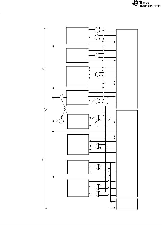
INFORMATION ADVANCE
TMS320C6678
Multicore Fixed and Floating-Point Digital Signal Processor
SPRS691—November 2010 |
www.ti.com |
|
Figure 2-1 shows the DSP core functional units and data paths.
Figure 2-1 TMS320C6678 DSP Core Data Paths
Note: |
|
src1 |
|
|
|
Default bus width |
|
|
|
|
|
|
|
|
|
|
|
is 64 bits |
.L1 |
|
|
|
|
(i.e. a register pair) |
src2 |
|
|
Register |
|
|
|
|
|
File A |
|
|
|
|
|
|
|
|
|
dst |
|
|
(A0, A1, A2, |
ST1 |
|
|
|
|
...A31) |
|
|
|
|
|
|
|
|
src1 |
|
|
|
|
.S1 |
src2 |
|
|
|
|
|
dst |
|
|
|
Data Path A |
|
src1 |
|
|
|
|
src1_hi |
|
|
|
|
|
|
|
|
|
|
|
.M1 |
src2 |
|
|
|
|
src2_hi |
|
|
|
|
|
|
|
|
|
|
|
|
dst2 |
|
|
|
|
|
dst1 |
|
|
|
LD1 |
|
|
|
|
|
|
|
src1 |
|
32 |
|
|
|
|
|
|
|
DA1 |
.D1 |
dst |
|
32 |
|
|
|
|
|||
32 |
|
|
|
|
|
|
|
src2 |
|
|
|
|
|
|
32 |
32 |
|
|
|
|
|
|
|
|
|
|
|
|
2 |
|
|
|
|
|
1 |
|
|
src2 |
|
32 |
Register |
|
|
|
|
File B |
|
DA2 |
.D2 |
|
32 |
32 |
|
dst |
|
(B0, B1, B2, |
|||
32 |
|
32 |
|||
|
|
|
|
|
|
|
|
src1 |
|
32 |
...B31) |
|
|
|
|
|
|
LD2 |
|
|
|
|
|
|
|
dst1 |
|
|
|
|
|
dst2 |
|
|
|
|
|
src2_hi |
|
|
|
|
.M2 |
src2 |
|
|
|
|
|
|
|
|
|
|
|
src1_hi |
|
|
|
|
|
src1 |
|
|
|
Data Path B |
|
|
|
|
|
|
|
dst |
|
|
|
|
.S2 |
src2 |
|
|
|
|
|
src1 |
|
|
|
ST2 |
|
|
|
|
|
|
|
dst |
|
|
|
|
.L2 |
src2 |
|
|
|
|
|
|
|
|
|
|
|
src1 |
|
|
|
|
|
|
|
32 |
Control |
|
|
|
|
|
Register |
|
|
|
|
32 |
|
18 |
Device Overview |
Copyright 2010 Texas Instruments Incorporated |

TMS320C6678
Multicore Fixed and Floating-Point Digital Signal Processor
www.ti.com |
SPRS691—November 2010 |
|
2.3 Memory Map Summary
Table 2-2 shows the memory map address ranges of the TMS320C6678 device.
Table 2-2 |
Memory Map Summary for TMS320C6678 (Part 1 of 7) |
|
|
|||
|
Address |
|
|
|
|
|
Start |
|
End |
Bytes |
Description |
|
|
00000000 |
|
007FFFFF |
8M |
Reserved |
|
|
|
|
|
|
|
|
|
00800000 |
|
0087FFFF |
512K |
Local L2 SRAM |
|
|
|
|
|
|
|
|
|
00880000 |
|
00DFFFFF |
5M+512K |
Reserved |
|
|
|
|
|
|
|
|
|
00E00000 |
|
00E07FFF |
32K |
Local L1P SRAM |
|
|
|
|
|
|
|
|
INFORMATION |
00E08000 |
|
00EFFFFF |
1M-32K |
Reserved |
|
|
|
|
|
||||
|
|
|
|
|
|
|
00F00000 |
|
00F07FFF |
32K |
L1D SRAM |
|
|
|
|
|
|
|
|
|
00F08000 |
|
017FFFFF |
9M-32K |
Reserved |
|
|
|
|
|
|
|
|
|
01800000 |
|
01BFFFFF |
4M |
C66x CorePac Registers |
|
|
|
|
|
|
|
|
|
01C00000 |
|
01CFFFFF |
1M |
Reserved |
|
|
|
|
|
|
|
|
|
01D00000 |
|
01D0007F |
128 |
Tracer 0 |
|
|
|
|
|
|
|
|
|
01D00080 |
|
01D07FFF |
32K-128 |
Reserved |
|
|
|
|
|
|
|
|
|
01D08000 |
|
01D0807F |
128 |
Tracer 1 |
|
|
|
|
|
|
|
|
|
01D08080 |
|
01D0FFFF |
32K-128 |
Reserved |
|
|
|
|
|
|
|
|
|
01D10000 |
|
01D1007F |
128 |
Tracer 2 |
|
ADVANCE |
|
|
|
|
|
|
|
01D10080 |
|
01D17FFF |
32K-128 |
Reserved |
|
|
|
|
|
||||
|
|
|
|
|
|
|
01D18000 |
|
01D1807F |
128 |
Tracer3 |
|
|
|
|
|
|
|
|
|
01D18080 |
|
01D1FFFF |
32K-128 |
Reserved |
|
|
|
|
|
|
|
|
|
01D20000 |
|
01D2007F |
128 |
Tracer 4 |
|
|
|
|
|
|
|
|
|
01D20080 |
|
01D27FFF |
32K-128 |
Reserved |
|
|
|
|
|
|
|
|
|
01D28000 |
|
01D2807F |
128 |
Tracer 5 |
|
|
|
|
|
|
|
|
|
01D28080 |
|
01D2FFFF |
32K-128 |
Reserved |
|
|
|
|
|
|
|
|
|
01D30000 |
|
01D3007F |
128 |
Tracer 6 |
|
|
|
|
|
|
|
|
|
01D30080 |
|
01D37FFF |
32K-128 |
Reserved |
|
|
|
|
|
|
|
|
|
01D38000 |
|
01D3807F |
128 |
Tracer 7 |
|
|
|
|
|
|
|
|
|
01D38080 |
|
01D3FFFF |
32K-128 |
Reserved |
|
|
|
|
|
|
|
|
|
01D40000 |
|
01D4007F |
128 |
Tracer 8 |
|
|
|
|
|
|
|
|
|
01D40080 |
|
01D47FFF |
32K-128 |
Reserved |
|
|
|
|
|
|
|
|
|
01D48000 |
|
01D4807F |
128 |
Tracer 9 |
|
|
|
|
|
|
|
|
|
01D48080 |
|
01D4FFFF |
32K-128 |
Reserved |
|
|
|
|
|
|
|
|
|
01D50000 |
|
01D5007F |
128 |
Tracer 10 |
|
|
|
|
|
|
|
|
|
01D50080 |
|
01D57FFF |
32K-128 |
Reserved |
|
|
|
|
|
|
|
|
|
01D58000 |
|
01D5807F |
128 |
Tracer 11 |
|
|
|
|
|
|
|
|
|
01D58080 |
|
01D5FFFF |
32K-128 |
Reserved |
|
|
|
|
|
|
|
|
|
01D60000 |
|
01D6007F |
128 |
Tracer 12 |
|
|
|
|
|
|
|
|
|
01D60080 |
|
01D67FFF |
32K-128 |
Reserved |
|
|
|
|
|
|
|
|
|
01D68000 |
|
01D6807F |
128 |
Tracer 13 |
|
|
|
|
|
|
|
|
|
01D68080 |
|
01D6FFFF |
32K-128 |
Reserved |
|
|
|
|
|
|
|
|
|
01D70000 |
|
01D7007F |
128 |
Tracer 14 |
|
|
|
|
|
|
|
|
|
01D70080 |
|
01D77FFF |
32K-128 |
Reserved |
|
|
|
|
|
|
|
|
|
01D78000 |
|
01D7807F |
128 |
Tracer 15 |
|
|
|
|
|
|
|
|
|
|
|
|
|
|
|
|
Copyright 2010 Texas Instruments Incorporated |
Device Overview |
19 |
|
|||

|
TMS320C6678 |
|
|
|||
|
Multicore Fixed and Floating-Point Digital Signal Processor |
|||||
|
SPRS691—November 2010 |
|
www.ti.com |
|||
|
|
|
|
|
|
|
|
Table 2-2 |
Memory Map Summary for TMS320C6678 (Part 2 of 7) |
||||
|
|
|
|
|
|
|
|
|
|
Address |
|
|
|
|
Start |
|
|
End |
Bytes |
Description |
|
01D78080 |
|
01D7FFFF |
32K-128 |
Reserved |
|
|
|
|
|
|
|
|
|
01D80000 |
|
01D8007F |
128 |
Tracer 16 |
|
|
|
|
|
|
|
|
|
01D80080 |
|
01DFFFFF |
512K-128 |
Reserved |
|
|
|
|
|
|
|
|
|
01E00000 |
|
01E3FFFF |
256K |
Telecom Serial Interface Port (TSIP) 0 |
|
|
|
|
|
|
|
|
|
01E40000 |
|
01E7FFFF |
256K |
Reserved |
|
|
|
|
|
|
|
|
|
01E80000 |
|
01EBFFFF |
256K |
Telecom Serial Interface Port (TSIP) 1 |
|
|
|
|
|
|
|
|
ADVANCE |
01EC0000 |
|
01FFFFFF |
1M +256K |
Reserved |
|
|
|
|
|
|
|
|
02000000 |
|
0209FFFF |
640K |
Packet Accelerator Subsystem Configuration |
||
|
|
|||||
|
|
|
|
|
|
|
|
020A0000 |
|
021FFFFF |
1M + 384K |
Reserved |
|
|
|
|
|
|
|
|
|
02200000 |
|
0220007F |
128 |
Timer0 |
|
|
|
|
|
|
|
|
|
02200080 |
|
0220FFFF |
64K-128 |
Reserved |
|
|
|
|
|
|
|
|
|
02210000 |
|
0221007F |
128 |
Timer1 |
|
|
|
|
|
|
|
|
|
02210080 |
|
0221FFFF |
64K-128 |
Reserved |
|
INFORMATION |
|
|
|
|
|
|
02220000 |
|
0222007F |
128 |
Timer2 |
||
|
|
|
|
|
||
02260080 |
|
0226FFFF |
64K-128 |
Reserved |
||
|
02220080 |
|
0222FFFF |
64K-128 |
Reserved |
|
|
02230000 |
|
0223007F |
128 |
Timer3 |
|
|
02230080 |
|
0223FFFF |
64K-128 |
Reserved |
|
|
02240000 |
|
0224007F |
128 |
Timer4 |
|
|
02240080 |
|
0224FFFF |
64K-128 |
Reserved |
|
|
02250000 |
|
0225007F |
128 |
Timer5 |
|
|
|
|
|
|
|
|
|
02250080 |
|
0225FFFF |
64K-128 |
Reserved |
|
|
|
|
|
|
|
|
|
02260000 |
|
0226007F |
128 |
Timer6 |
|
|
|
|
|
|
|
|
|
|
|
|
|
|
|
|
02270000 |
|
0227007F |
128 |
Timer7 |
|
|
|
|
|
|
|
|
|
02270080 |
|
0227FFFF |
64K-128 |
Reserved |
|
|
|
|
|
|
|
|
|
02280000 |
|
0228007F |
128 |
Timer8 |
|
|
|
|
|
|
|
|
|
02280080 |
|
0228FFFF |
64K-128 |
Reserved |
|
|
|
|
|
|
|
|
|
02290000 |
|
0229007F |
128 |
Timer9 |
|
|
|
|
|
|
|
|
|
02290080 |
|
0229FFFF |
64K-128 |
Reserved |
|
|
|
|
|
|
|
|
|
022A0000 |
|
022A007F |
128 |
Timer10 |
|
|
|
|
|
|
|
|
|
022A0080 |
|
022AFFFF |
64K-128 |
Reserved |
|
|
|
|
|
|
|
|
|
022B0000 |
|
022B007F |
128 |
Timer11 |
|
|
|
|
|
|
|
|
|
022B0080 |
|
022BFFFF |
64K-128 |
Reserved |
|
|
|
|
|
|
|
|
|
022C0000 |
|
022C007F |
128 |
Timer12 |
|
|
|
|
|
|
|
|
|
022C0080 |
|
022CFFFF |
64K-128 |
Reserved |
|
|
|
|
|
|
|
|
|
022D0000 |
|
022D007F |
128 |
Timer13 |
|
|
|
|
|
|
|
|
|
022D0080 |
|
022DFFFF |
64K-128 |
Reserved |
|
|
|
|
|
|
|
|
|
022E0000 |
|
022E007F |
128 |
Timer14 |
|
|
|
|
|
|
|
|
|
022E0080 |
|
022EFFFF |
64K-128 |
Reserved |
|
|
|
|
|
|
|
|
|
022F0000 |
|
022F007F |
128 |
Timer15 |
|
|
|
|
|
|
|
|
|
022F0080 |
|
022FFFFF |
64K-128 |
Reserved |
|
|
|
|
|
|
|
|
|
02300000 |
|
0230FFFF |
64K |
Reserved |
|
|
|
|
|
|
|
|
|
02310000 |
|
023101FF |
512 |
PLL Controller |
|
|
|
|
|
|
|
|
|
|
|
|
|
|
|
|
20 |
Device Overview |
|
Copyright 2010 Texas Instruments Incorporated |
||
|
|
|
|
|
TMS320C6678 |
||
|
|
|
|
Multicore Fixed and Floating-Point Digital Signal Processor |
|||
www.ti.com |
|
|
|
|
SPRS691—November 2010 |
||
|
|
|
|
|
|
|
|
Table 2-2 |
Memory Map Summary for TMS320C6678 (Part 3 of 7) |
|
|
||||
|
|
|
|
|
|
|
|
|
Address |
|
|
|
|
|
|
Start |
|
End |
Bytes |
|
Description |
|
|
02310200 |
|
0231FFFF |
64K-512 |
|
Reserved |
|
|
|
|
|
|
|
|
|
|
02320000 |
|
023200FF |
256 |
|
GPIO |
|
|
|
|
|
|
|
|
|
|
02320100 |
|
0232FFFF |
64K-256 |
|
Reserved |
|
|
|
|
|
|
|
|
|
|
02330000 |
|
023303FF |
1K |
|
SmartRlex |
|
|
|
|
|
|
|
|
|
|
02330400 |
|
0234FFFF |
127K |
|
Reserved |
|
|
|
|
|
|
|
|
|
|
02350000 |
|
02350FFF |
4K |
|
Power Sleep Controller (PSC) |
|
|
|
|
|
|
|
|
|
|
02351000 |
|
0235FFFF |
64K-4K |
|
Reserved |
|
INFORMATION |
|
|
|
|
|
|
|
|
02360000 |
|
023603FF |
1K |
|
Memory Protection Unit (MPU) 0 |
|
|
|
|
|
|
||||
|
|
|
|
|
|
|
|
02360400 |
|
02367FFF |
31K |
|
Reserved |
|
|
|
|
|
|
|
|
|
|
02368000 |
|
023683FF |
1K |
|
Memory Protection Unit (MPU) 1 |
|
|
|
|
|
|
|
|
|
|
02368400 |
|
0236FFFF |
31K |
|
Reserved |
|
|
|
|
|
|
|
|
|
|
02370000 |
|
023703FF |
1K |
|
Memory Protection Unit (MPU) 2 |
|
|
|
|
|
|
|
|
|
|
02370400 |
|
02377FFF |
31K |
|
Reserved |
|
|
|
|
|
|
|
|
|
|
02378000 |
|
023783FF |
1K |
|
Memory Protection Unit (MPU) 3 |
|
|
|
|
|
|
|
|
|
|
02378400 |
|
0237FFFF |
31K |
|
Reserved |
|
|
|
|
|
|
|
|
|
|
02380000 |
|
0243FFFF |
768K |
|
Reserved |
|
|
|
|
|
|
|
|
|
ADVANCE |
02440000 |
|
02443FFF |
16K |
|
DSP Trace Formatter 0 |
|
|
|
|
|
|
|
|
|
|
02470000 |
|
02473FFF |
16K |
|
DSP Trace Formatter 3 |
|
|
02444000 |
|
0244FFFF |
48K |
|
Reserved |
|
|
02450000 |
|
02453FFF |
16K |
|
DSP Trace Formatter 1 |
|
|
02454000 |
|
0245FFFF |
48K |
|
Reserved |
|
|
02460000 |
|
02463FFF |
16K |
|
DSP Trace Formatter 2 |
|
|
|
|
|
|
|
|
|
|
02464000 |
|
0246FFFF |
48K |
|
Reserved |
|
|
|
|
|
|
|
|
|
|
|
|
|
|
|
|
|
|
02474000 |
|
0247FFFF |
48K |
|
Reserved |
|
|
|
|
|
|
|
|
|
|
02480000 |
|
02483FFF |
16K |
|
DSP Trace Formatter 4 |
|
|
|
|
|
|
|
|
|
|
02484000 |
|
0248FFFF |
48K |
|
Reserved |
|
|
|
|
|
|
|
|
|
|
02490000 |
|
02493FFF |
16K |
|
DSP Trace Formatter 5 |
|
|
|
|
|
|
|
|
|
|
02494000 |
|
0249FFFF |
48K |
|
Reserved |
|
|
|
|
|
|
|
|
|
|
024A0000 |
|
024A3FFF |
16K |
|
DSP Trace Formatter 6 |
|
|
|
|
|
|
|
|
|
|
024A4000 |
|
024AFFFF |
48K |
|
Reserved |
|
|
|
|
|
|
|
|
|
|
024B0000 |
|
024B3FFF |
16K |
|
DSP Trace Formatter 7 |
|
|
|
|
|
|
|
|
|
|
024B4000 |
|
024BFFFF |
48K |
|
Reserved |
|
|
|
|
|
|
|
|
|
|
024C0000 |
|
0252FFFF |
448K |
|
Reserved |
|
|
|
|
|
|
|
|
|
|
02530000 |
|
0253007F |
128 |
|
I2C Data & Control |
|
|
02530080 |
|
0253FFFF |
64K-128 |
|
Reserved |
|
|
|
|
|
|
|
|
|
|
02540000 |
|
0254003F |
64 |
|
UART |
|
|
|
|
|
|
|
|
|
|
02540400 |
|
0254FFFF |
64K-64 |
|
Reserved |
|
|
|
|
|
|
|
|
|
|
02550000 |
|
025FFFFF |
704K |
|
Reserved |
|
|
|
|
|
|
|
|
|
|
02600000 |
|
02601FFF |
8K |
|
Secondary Interrupt Controller (INTC) 0 |
|
|
|
|
|
|
|
|
|
|
02602000 |
|
02603FFF |
8K |
|
Reserved |
|
|
|
|
|
|
|
|
|
|
02604000 |
|
02605FFF |
8K |
|
Secondary Interrupt Controller (INTC) 1 |
|
|
|
|
|
|
|
|
|
|
02606000 |
|
02607FFF |
8K |
|
Reserved |
|
|
|
|
|
|
|
|
|
|
02608000 |
|
02609FFF |
8K |
|
Secondary Interrupt Controller (INTC) 2 |
|
|
|
|
|
|
|
|
|
|
|
|
|
|
|
|
|
|
Copyright 2010 Texas Instruments Incorporated |
|
Device Overview |
21 |
|
|||

|
TMS320C6678 |
|
|
||
|
Multicore Fixed and Floating-Point Digital Signal Processor |
||||
|
SPRS691—November 2010 |
|
www.ti.com |
||
|
|
|
|
|
|
|
Table 2-2 |
Memory Map Summary for TMS320C6678 (Part 4 of 7) |
|||
|
|
|
|
|
|
|
|
Address |
|
|
|
|
Start |
|
End |
Bytes |
Description |
|
0260A000 |
|
0260BFFF |
8K |
Reserved |
|
|
|
|
|
|
|
0260C000 |
|
0260DFFF |
8K |
Secondary Interrupt Controller (INTC) 3 |
|
|
|
|
|
|
|
0260E000 |
|
0261FFFF |
72K |
Reserved |
|
|
|
|
|
|
|
02620000 |
|
026207FF |
2K |
Chip-Level Registers (boot cfg) |
|
|
|
|
|
|
|
02620800 |
|
0263FFFF |
126K |
Reserved |
|
|
|
|
|
|
|
02640000 |
|
026407FF |
2K |
Semaphore |
|
|
|
|
|
|
ADVANCE |
02640800 |
|
0264FFFF |
64K-2K |
Reserved |
|
|
|
|
|
|
02650000 |
|
026FFFFF |
704K |
Reserved |
|
|
|
||||
|
|
|
|
|
|
|
02700000 |
|
02707FFF |
32K |
EDMA Channel Controller (TPCC) 0 |
|
|
|
|
|
|
|
02708000 |
|
0271FFFF |
96K |
Reserved |
|
|
|
|
|
|
|
02720000 |
|
02727FFF |
32K |
EDMA Channel Controller (TPCC) 1 |
|
|
|
|
|
|
|
02728000 |
|
0273FFFF |
96K |
Reserved |
|
|
|
|
|
|
|
02740000 |
|
02747FFF |
32K |
EDMA Channel Controller (TPCC) 2 |
INFORMATION |
|
|
|
|
|
02748000 |
|
0275FFFF |
96K |
Reserved |
|
|
|
|
|
|
|
02780000 |
|
027803FF |
1K |
EDMA TPCC1 Transfer Controller (TPTC) 2 |
|
|
02760000 |
|
027603FF |
1K |
EDMA TPCC0 Transfer Controller (TPTC) 0 |
|
02760400 |
|
02767FFF |
31K |
Reserved |
|
02768000 |
|
027683FF |
1K |
EDMA TPCC0 Transfer Controller (TPTC) 1 |
|
02768400 |
|
0276FFFF |
31K |
Reserved |
|
02770000 |
|
027703FF |
1K |
EDMA TPCC1 Transfer Controller (TPTC) 0 |
|
02770400 |
|
02777FFF |
31K |
Reserved |
|
|
|
|
|
|
|
02778000 |
|
027783FF |
1K |
EDMA TPCC1 Transfer Controller (TPTC) 1 |
|
|
|
|
|
|
|
02780400 |
|
0277FFFF |
31K |
Reserved |
|
|
|
|
|
|
|
|
|
|
|
|
|
02780400 |
|
02787FFF |
31K |
Reserved |
|
|
|
|
|
|
|
02788000 |
|
027883FF |
1K |
EDMA TPCC1Transfer Controller (TPTC) 3 |
|
|
|
|
|
|
|
02788400 |
|
0278FFFF |
31K |
Reserved |
|
|
|
|
|
|
|
02790000 |
|
027903FF |
1K |
EDMA TPCC2 Transfer Controller (TPTC) 0 |
|
|
|
|
|
|
|
02790400 |
|
02797FFF |
31K |
Reserved |
|
|
|
|
|
|
|
02798000 |
|
027983FF |
1K |
EDMA TPCC2 Transfer Controller (TPTC) 1 |
|
|
|
|
|
|
|
02798400 |
|
0279FFFF |
31K |
Reserved |
|
|
|
|
|
|
|
027A0000 |
|
027A03FF |
1K |
EDMA TPCC2 Transfer Controller (TPTC) 2 |
|
|
|
|
|
|
|
027A0400 |
|
027A7FFF |
31K |
Reserved |
|
|
|
|
|
|
|
027A8000 |
|
027A83FF |
1K |
EDMA TPCC2 Transfer Controller (TPTC) 3 |
|
|
|
|
|
|
|
027A8400 |
|
027AFFFF |
31K |
Reserved |
|
|
|
|
|
|
|
027B0000 |
|
027CFFFF |
128K |
Reserved |
|
|
|
|
|
|
|
027D0000 |
|
027D3FFF |
16K |
TI Embedded Trace Buffer (TETB) core 0 |
|
|
|
|
|
|
|
027D4000 |
|
027DFFFF |
48K |
Reserved |
|
|
|
|
|
|
|
027E0000 |
|
027E3FFF |
16K |
TI Embedded Trace Buffer (TETB) core 1 |
|
|
|
|
|
|
|
027E4000 |
|
027EFFFF |
48K |
Reserved |
|
|
|
|
|
|
|
027F0000 |
|
027F3FFF |
16K |
TI Embedded Trace Buffer (TETB) core 2 |
|
|
|
|
|
|
|
027F4000 |
|
027FFFFF |
48K |
Reserved |
|
|
|
|
|
|
|
02800000 |
|
02803FFF |
16K |
TI Embedded Trace Buffer (TETB) core 3 |
|
|
|
|
|
|
|
02804000 |
|
0280FFFF |
48K |
Reserved |
|
|
|
|
|
|
|
|
|
|
|
|
|
22 Device Overview |
|
Copyright 2010 Texas Instruments Incorporated |
||

|
|
|
|
|
TMS320C6678 |
||
|
|
|
|
Multicore Fixed and Floating-Point Digital Signal Processor |
|||
www.ti.com |
|
|
|
|
SPRS691—November 2010 |
||
|
|
|
|
|
|
|
|
Table 2-2 |
Memory Map Summary for TMS320C6678 (Part 5 of 7) |
|
|
||||
|
|
|
|
|
|
|
|
|
Address |
|
|
|
|
|
|
Start |
|
End |
Bytes |
|
Description |
|
|
02810000 |
|
02813FFF |
16K |
|
TI Embedded Trace Buffer (TETB) core 4 |
|
|
|
|
|
|
|
|
|
|
02814000 |
|
0281FFFF |
48K |
|
Reserved |
|
|
|
|
|
|
|
|
|
|
02820000 |
|
02823FFF |
16K |
|
TI Embedded Trace Buffer (TETB) core 5 |
|
|
|
|
|
|
|
|
|
|
02824000 |
|
0282FFFF |
48K |
|
Reserved |
|
|
|
|
|
|
|
|
|
|
02830000 |
|
02833FFF |
16K |
|
TI Embedded Trace Buffer (TETB) core 6 |
|
|
|
|
|
|
|
|
|
|
02834000 |
|
0283FFFF |
48K |
|
Reserved |
|
|
|
|
|
|
|
|
|
|
02840000 |
|
02843FFF |
16K |
|
TI Embedded Trace Buffer (TETB) core 7 |
|
INFORMATION |
|
|
|
|
|
|
|
|
02844000 |
|
0284FFFF |
48K |
|
Reserved |
|
|
|
|
|
|
||||
|
|
|
|
|
|
|
|
02850000 |
|
02857FFF |
32K |
|
TI Embedded Trace Buffer (TETB) — system |
|
|
|
|
|
|
|
|
|
|
02858000 |
|
0285FFFF |
32K |
|
Reserved |
|
|
|
|
|
|
|
|
|
|
02860000 |
|
028FFFFF |
640K |
|
Reserved |
|
|
|
|
|
|
|
|
|
|
02900000 |
|
02907FFF |
32K |
|
Serial RapidIO (SRIO) Configuration |
|
|
|
|
|
|
|
|
|
|
02908000 |
|
029FFFFF |
1M-32K |
|
Reserved |
|
|
|
|
|
|
|
|
|
|
02A00000 |
|
02BFFFFF |
2M |
|
Queue Manager Subsystem Configuration |
|
|
|
|
|
|
|
|
|
|
02C00000 |
|
07FFFFFF |
84M |
|
Reserved |
|
|
|
|
|
|
|
|
|
|
08000000 |
|
0800FFFF |
64K |
|
Extended Memory Controller (XMC) Configuration |
|
|
|
|
|
|
|
|
|
ADVANCE |
08010000 |
|
0BBFFFFF |
60M-64K |
|
Reserved |
|
|
|
|
|
|
|
|
|
|
0BC00000 |
|
0BCFFFFF |
1M |
|
Multicore Shared Memory Controller (MSMC) Config |
|
|
|
|
|
|
|
|
|
|
0BD00000 |
|
0BFFFFFF |
3M |
|
Reserved |
|
|
|
|
|
|
|
|
|
|
0C000000 |
|
0C3FFFFF |
4M |
|
Multicore Shared Memory |
|
|
|
|
|
|
|
|
|
|
0C400000 |
|
107FFFFF |
68 M |
|
Reserved |
|
|
|
|
|
|
|
|
|
|
10800000 |
|
1087FFFF |
512K |
|
Core0 L2 SRAM |
|
|
|
|
|
|
|
|
|
|
10880000 |
|
108FFFFF |
512K |
|
Reserved |
|
|
|
|
|
|
|
|
|
|
10900000 |
|
10DFFFFF |
5M |
|
Reserved |
|
|
|
|
|
|
|
|
|
|
10E00000 |
|
10E07FFF |
32K |
|
Core0 L1P SRAM |
|
|
|
|
|
|
|
|
|
|
10E08000 |
|
10EFFFFF |
1M-32K |
|
Reserved |
|
|
|
|
|
|
|
|
|
|
10F00000 |
|
10F07FFF |
32K |
|
Core0 L1D SRAM |
|
|
|
|
|
|
|
|
|
|
10F08000 |
|
117FFFFF |
9M-32K |
|
Reserved |
|
|
|
|
|
|
|
|
|
|
11800000 |
|
1187FFFF |
512K |
|
Core1 L2 SRAM |
|
|
|
|
|
|
|
|
|
|
11880000 |
|
118FFFFF |
512K |
|
Reserved |
|
|
|
|
|
|
|
|
|
|
11900000 |
|
11DFFFFF |
5M |
|
Reserved |
|
|
|
|
|
|
|
|
|
|
11E00000 |
|
11E07FFF |
32K |
|
Core1 L1P SRAM |
|
|
|
|
|
|
|
|
|
|
11E08000 |
|
11EFFFFF |
1M-32K |
|
Reserved |
|
|
|
|
|
|
|
|
|
|
11F00000 |
|
11F07FFF |
32K |
|
Core1 L1D SRAM |
|
|
|
|
|
|
|
|
|
|
11F08000 |
|
127FFFFF |
9M-32K |
|
Reserved |
|
|
|
|
|
|
|
|
|
|
12800000 |
|
1287FFFF |
512K |
|
Core2 L2 SRAM |
|
|
|
|
|
|
|
|
|
|
12880000 |
|
128FFFFF |
512K |
|
Reserved |
|
|
|
|
|
|
|
|
|
|
12900000 |
|
12DFFFFF |
5M |
|
Reserved |
|
|
|
|
|
|
|
|
|
|
12E00000 |
|
12E07FFF |
32K |
|
Core2 L1P SRAM |
|
|
|
|
|
|
|
|
|
|
12E08000 |
|
12EFFFFF |
1M-32K |
|
Reserved |
|
|
|
|
|
|
|
|
|
|
12F00000 |
|
12F07FFF |
32K |
|
Core2 L1D SRAM |
|
|
|
|
|
|
|
|
|
|
12F08000 |
|
137FFFFF |
9M-32K |
|
Reserved |
|
|
|
|
|
|
|
|
|
|
13800000 |
|
1387FFFF |
512K |
|
Core3 L2 SRAM |
|
|
|
|
|
|
|
|
|
|
|
|
|
|
|
|
|
|
Copyright 2010 Texas Instruments Incorporated |
|
Device Overview |
23 |
|
|||

|
TMS320C6678 |
|
|
||
|
Multicore Fixed and Floating-Point Digital Signal Processor |
||||
|
SPRS691—November 2010 |
|
www.ti.com |
||
|
|
|
|
|
|
|
Table 2-2 |
Memory Map Summary for TMS320C6678 (Part 6 of 7) |
|||
|
|
|
|
|
|
|
|
Address |
|
|
|
|
Start |
|
End |
Bytes |
Description |
|
13880000 |
|
138FFFFF |
512K |
Reserved |
|
|
|
|
|
|
|
13900000 |
|
13DFFFFF |
5M |
Reserved |
|
|
|
|
|
|
|
13E00000 |
|
13E07FFF |
32K |
Core3 L1P SRAM |
|
|
|
|
|
|
|
13E08000 |
|
13EFFFFF |
1M-32K |
Reserved |
|
|
|
|
|
|
|
13F00000 |
|
13F07FFF |
32K |
Core3 L1D SRAM |
|
|
|
|
|
|
|
13F08000 |
|
147FFFFF |
9M-32K |
Reserved |
|
|
|
|
|
|
ADVANCE |
14800000 |
|
1487FFFF |
512K |
Core4 L2 SRAM |
|
|
|
|
|
|
14880000 |
|
148FFFFF |
512K |
Reserved |
|
|
|
||||
|
|
|
|
|
|
|
14900000 |
|
14DFFFFF |
5M |
Reserved |
|
|
|
|
|
|
|
14E00000 |
|
14E07FFF |
32K |
Core4 L1P SRAM |
|
|
|
|
|
|
|
14E08000 |
|
14EFFFFF |
1M-32K |
Reserved |
|
|
|
|
|
|
|
14F00000 |
|
14F07FFF |
32K |
Core4 L1D SRAM |
|
|
|
|
|
|
|
14F08000 |
|
157FFFFF |
9M-32K |
Reserved |
INFORMATION |
|
|
|
|
|
15800000 |
|
1587FFFF |
512K |
Core5 L2 SRAM |
|
|
|
|
|
|
|
16900000 |
|
16DFFFFF |
5M |
Reserved |
|
|
15880000 |
|
158FFFFF |
512K |
Reserved |
|
15900000 |
|
15DFFFFF |
5M |
Reserved |
|
15E00000 |
|
15E07FFF |
32K |
Core5 L1P SRAM |
|
15E08000 |
|
15EFFFFF |
1M-32K |
Reserved |
|
15F00000 |
|
15F07FFF |
32K |
Core5 L1D SRAM |
|
15F08000 |
|
167FFFFF |
9M-32K |
Reserved |
|
|
|
|
|
|
|
16800000 |
|
1687FFFF |
512K |
Core6 L2 SRAM |
|
|
|
|
|
|
|
16880000 |
|
168FFFFF |
512K |
Reserved |
|
|
|
|
|
|
|
|
|
|
|
|
|
16E00000 |
|
16E07FFF |
32K |
Core6 L1P SRAM |
|
|
|
|
|
|
|
16E08000 |
|
16EFFFFF |
1M-32K |
Reserved |
|
|
|
|
|
|
|
16F00000 |
|
16F07FFF |
32K |
Core6 L1D SRAM |
|
|
|
|
|
|
|
16F08000 |
|
177FFFFF |
9M-32K |
Reserved |
|
|
|
|
|
|
|
17800000 |
|
1787FFFF |
512K |
Core7 L2 SRAM |
|
|
|
|
|
|
|
17880000 |
|
178FFFFF |
512K |
Reserved |
|
|
|
|
|
|
|
17900000 |
|
17DFFFFF |
5M |
Reserved |
|
|
|
|
|
|
|
17E00000 |
|
17E07FFF |
32K |
Core7 L1P SRAM |
|
|
|
|
|
|
|
17E08000 |
|
17EFFFFF |
1M-32K |
Reserved |
|
|
|
|
|
|
|
17F00000 |
|
17F07FFF |
32K |
Core7 L1D SRAM |
|
|
|
|
|
|
|
17F08000 |
|
1FFFFFFF |
129M-32K |
Reserved |
|
|
|
|
|
|
|
20000000 |
|
200FFFFF |
1M |
System Trace Manager (STM) Configuration |
|
|
|
|
|
|
|
20100000 |
|
20AFFFFF |
10M |
Reserved |
|
|
|
|
|
|
|
20B00000 |
|
20B1FFFF |
128K |
Boot ROM |
|
|
|
|
|
|
|
20B20000 |
|
20BEFFFF |
832K |
Reserved |
|
|
|
|
|
|
|
20BF0000 |
|
20BF03FF |
1K |
SPI |
|
|
|
|
|
|
|
20BF0400 |
|
20BFFFFF |
63K |
Reserved |
|
|
|
|
|
|
|
20C00000 |
|
20C000FF |
256 |
EMIF-16 Config |
|
|
|
|
|
|
|
20C00100 |
|
20FFFFFF |
12M - 256 |
Reserved |
|
|
|
|
|
|
|
21000000 |
|
210000FF |
256 |
DDR3 EMIF Configuration |
|
|
|
|
|
|
|
|
|
|
|
|
|
24 Device Overview |
|
Copyright 2010 Texas Instruments Incorporated |
||

|
|
|
|
|
TMS320C6678 |
|
|
|
|
|
Multicore Fixed and Floating-Point Digital Signal Processor |
|
|
www.ti.com |
|
|
|
|
SPRS691—November 2010 |
|
|
|
|
|
|
|
|
Table 2-2 |
Memory Map Summary for TMS320C6678 (Part 7 of 7) |
|
||||
|
|
|
|
|
|
|
|
Address |
|
|
|
|
|
Start |
|
End |
Bytes |
|
Description |
|
21000100 |
|
213FFFFF |
4M-256 |
|
Reserved |
|
|
|
|
|
|
|
|
21400000 |
|
214003FF |
1K |
|
HyperLink Config |
|
|
|
|
|
|
|
|
21400400 |
|
217FFFFF |
4M-1K |
|
Reserved |
|
|
|
|
|
|
|
|
21800000 |
|
21807FFF |
32K |
|
PCIe Config |
|
|
|
|
|
|
|
|
21808000 |
|
33FFFFFF |
296M-32K |
|
Reserved |
|
|
|
|
|
|
|
|
34000000 |
|
341FFFFF |
2M |
|
Queue Manager Subsystem Data |
|
|
|
|
|
|
|
|
34200000 |
|
3FFFFFFF |
190M |
|
Reserved |
INFORMATION |
|
|
|
|
|
|
|
40000000 |
|
4FFFFFFF |
256M |
|
HyperLink data |
|
|
|
|
||||
|
|
|
|
|
|
|
50000000 |
|
5FFFFFFF |
256M |
|
Reserved |
|
|
|
|
|
|
|
|
60000000 |
|
6FFFFFFF |
256M |
|
PCIe Data |
|
|
|
|
|
|
|
|
70000000 |
|
73FFFFFF |
64M |
|
EMIF16 CS2 Data NAND Memory |
|
|
|
|
|
|
|
|
74000000 |
|
77FFFFFF |
64M |
|
EMIF16 CS3 Data NAND Memory |
|
|
|
|
|
|
|
|
78000000 |
|
7BFFFFFF |
64M |
|
EMIF16 CS4 Data NOR Memory |
|
|
|
|
|
|
|
|
7C000000 |
|
7FFFFFFF |
64M |
|
EMIF16 CS5 Data SRAM Memory |
|
|
|
|
|
|
|
|
80000000 |
|
8FFFFFFF |
256M |
|
DDR3_ Data |
|
|
|
|
|
|
|
|
90000000 |
|
9FFFFFFF |
256M |
|
DDR3_ Data |
|
|
|
|
|
|
|
ADVANCE |
A0000000 |
|
AFFFFFFF |
256M |
|
DDR3_ Data |
|
|
|
|
|
|
|
|
B0000000 |
|
BFFFFFFF |
256M |
|
DDR3_ Data |
|
|
|
|
||||
|
|
|
|
|
|
|
C0000000 |
|
CFFFFFFF |
256M |
|
DDR3_ Data |
|
|
|
|
|
|
|
|
D0000000 |
|
DFFFFFFF |
256M |
|
DDR3_ Data |
|
|
|
|
|
|
|
|
E0000000 |
|
EFFFFFFF |
256M |
|
DDR3_ Data |
|
|
|
|
|
|
|
|
F0000000 |
|
FFFFFFFF |
256M |
|
DDR3_ Data |
|
|
|
|
|
|
|
|
End of Table 2-2 |
|
|
|
|
||
|
|
|
|
|
|
|
2.4 Boot Sequence
The boot sequence is a process by which the DSP's internal memory is loaded with program and data sections. The DSP's internal registers are programmed with predetermined values. The boot sequence is started automatically after each power-on reset, warm reset, and system reset. A local reset to an individual C66x CorePac should not affect the state of the hardware boot controller on the device. For more details on the initiators of the resets, see section ‘‘Reset Controller’’.
The C6678 supports several boot processes that begins execution at the ROM base address, which contains the bootloader code necessary to support various device boot modes. The boot processes are software-driven and use the BOOTMODE[12:0] device configuration inputs to determine the software configuration that must be completed. For more details on Boot Sequence see the Bootloader for the C66x DSP User Guide (literature number SPRUGY5).
Copyright 2010 Texas Instruments Incorporated |
Device Overview |
25 |
INFORMATION ADVANCE
TMS320C6678
Multicore Fixed and Floating-Point Digital Signal Processor
SPRS691—November 2010 |
www.ti.com |
|
2.5 Boot Modes Supported and PLL Settings
The device supports several boot processes, which leverage the internal boot ROM. Most boot processes are software driven, using the BOOTMODE[3:0] device configuration inputs to determine the software configuration that must be completed. From a hardware perspective, there are two possible boot modes:
•Public ROM Boot - C66x CorePac 0 is released from reset and begins executing from the L3 ROM base address. After performing the boot process (e.g., from I2C ROM, Ethernet, or RapidIO), the C66x CorePac 0 then begins execution from the provided boot entry point, other C66x CorePac’s are released from reset based on interrupts generated by C66x CorePac 0, see the Bootloader for the C66x DSP User Guide (literature number SPRUGY5) for more details.
•Secure ROM Boot - On secure devices, the C66x CorePac 0 is released from reset and begin executing from secure ROM. Software in the secure ROM will free up internal RAM pages, after which the C66x CorePac 0 initiates the boot process. The C66x CorePac 0 performs any authentication and decryption required on the bootloaded image prior to beginning execution.
The boot process performed by the C66x CorePac 0 in public ROM boot and secure ROM boot are determined by the BOOTMODE[12:0] value in the DEVSTAT register. The C66x CorePac 0 reads this value, and then executes the associated boot process in software. Figure 2-2 shows the bits associated with BOOTMODE[12:0].
Figure 2-2 |
Boot Mode Pin Decoding |
|
|
|
|
|
|
|
|
|
|
|
|
|||||
|
|
|
|
|
|
|
|
|
|
|
|
|
|
|
|
|
|
|
|
|
|
|
|
|
|
|
|
Boot Mode Pins |
|
|
|
|
|
|
|
||
12 |
|
11 |
|
10 |
9 |
|
8 |
7 |
|
6 |
|
5 |
4 |
3 |
2 |
1 |
|
0 |
|
|
PLL Mult |
|
|
|
|
|
Device Configuration |
|
|
|
|
Boot Device |
|
||||
I2C /SPI Ext Dev Cfg |
|
|
|
|
|
|
|
|
|
|
|
|
|
|||||
2.5.1 Boot Device Field
The Boot Device field BOOTMODE[2:0] defines the boot device that is chosen. Table 2-3 shows the supported boot modes.
Table 2-3 Boot Mode Pins: Boot Device Values
Bit |
Field |
Value |
Description |
2-0 |
Boot Device |
0 |
Sleep / test modes / EMIF16 |
|
|
|
|
|
|
1 |
Serial Rapid I/O |
|
|
|
|
|
|
2 |
Ethernet (SGMII) (PA driven from core clk) |
|
|
|
|
|
|
3 |
Ethernet (SGMII) (PA driver from PA clk) |
4PCI
5I2C
6SPI
7HyperLink
26 |
Device Overview |
Copyright 2010 Texas Instruments Incorporated |

TMS320C6678
Multicore Fixed and Floating-Point Digital Signal Processor
www.ti.com |
SPRS691—November 2010 |
|
2.5.2 Device Configuration Field
The device configuration fields BOOTMODE[9:3] are used to configure the boot peripheral and, therefore, the bit definitions depend on the boot mode
2.5.2.1 Sleep / EMIF16 Boot Device Configuration
Figure 2-3 |
Sleep / EMIF16 Configuration Bit Fields |
|
|
|
|
|
|
|
|||||
|
|
|
|
|
|
|
|
|
|
|
|
|
|
|
9 |
|
|
8 |
|
7 |
6 |
|
5 |
4 |
|
3 |
|
|
|
Reserved |
|
|
Wait Enable |
|
Sub-Mode |
|
Reserved |
|
|||
|
|
|
|
|
|
|
|
|
|
|
|
|
|
Table 2-4 |
Sleep / EMIF16 Configuration Bit Field Descriptions |
|
|
|
|
|
|
||||||
|
|
|
|
|
|
|
|
|
|
|
|
|
|
Bit |
Field |
|
|
Value |
Description |
|
|
|
|
|
|
|
|
9-8 |
Reserved |
0-3 |
|
Reserved |
|
|
|
|
|
|
|
||
|
|
|
|
|
|
|
|
|
|||||
7 |
Wait Enable |
0 |
|
Wait enable disabled (EMIF16 sub mode) |
|
|
|
|
|||||
|
|
|
|
1 |
|
Wait enable enabled (EMIF16 sub mode) |
|
|
|
|
|||
|
|
|
|
|
|
|
|
|
|
|
|
||
6-5 |
Sub-Mode |
0 |
|
Sleep boot |
|
|
|
|
|
|
|
||
|
|
|
|
1 |
|
EMIF16 boot |
|
|
|
|
|
|
|
|
|
|
|
|
|
|
|
|
|
|
|
||
4-3 |
Reserved |
0-3 |
|
Reserved |
|
|
|
|
|
|
|
||
|
|
|
|
|
|
|
|
|
|
|
|
|
|
2.5.2.2 Ethernet (SGMII) Boot Device Configuration
Figure 2-4 |
Ethernet (SGMII) Device Configuration Bit Fields |
|
|
|
|
|
||||||||||
|
|
|
|
|
|
|
|
|
|
|
|
|
|
|
|
|
|
|
9 |
|
|
8 |
|
7 |
|
6 |
|
5 |
|
4 |
|
3 |
|
|
|
|
SerDes Clock Mult |
|
|
|
Ext connection |
|
|
Device ID |
|
|
Reserved |
|||
|
|
|
|
|
|
|
|
|
|
|
|
|
|
|
||
Table 2-5 |
Ethernet (SGMII) Configuration Bit Field Descriptions |
|
|
|
|
|
||||||||||
|
|
|
|
|
|
|
|
|
|
|
|
|
|
|
|
|
|
Bit |
Field |
|
Value |
|
|
|
|
Description |
|
|
|
||||
|
9-8 |
SerDes Clock Mult |
|
|
|
The output frequency of the PLL must be 1.25 GBs. |
|
|
|
|||||||
|
|
|
|
|
|
0 |
|
×8 for input clock of 156.25 MHz |
|
|
|
|
|
|||
|
|
|
|
|
|
1 |
|
×5 for input clock of 250 MHz |
|
|
|
|
|
|
|
|
|
|
|
|
|
|
2 |
|
×4 for input clock of 312.5 MHz |
|
|
|
|
|
|||
|
|
|
|
|
|
3 |
|
Reserved |
|
|
|
|
|
|
|
|
|
|
|
|
|
|
|
|
|
|
|||||||
|
7-6 |
Ext connection |
|
0 |
|
Mac to Mac connection, master with auto negotiation |
|
|
|
|||||||
|
|
|
|
|
|
1 |
|
Mac to Mac connection, slave, and Mac to Phy |
|
|
|
|
|
|||
|
|
|
|
|
|
2 |
|
Mac to Mac, forced link |
|
|
|
|
|
|
|
|
|
|
|
|
|
|
3 |
|
Mac to fiber connection |
|
|
|
|
|
|
|
|
|
|
|
|
|
|
|
|
|
|
|||||||
|
5 |
Device ID |
|
0-7 |
|
This value is used in the device ID field of the Ethernet-ready frame. |
|
|
|
|||||||
|
|
|
|
|
|
|
|
|
|
|
|
|
|
|||
|
4-3 |
Reserved |
|
0-3 |
|
Reserved |
|
|
|
|
|
|
|
|||
|
|
|
|
|
|
|
|
|
|
|
|
|
|
|
|
|
ADVANCE INFORMATION
Copyright 2010 Texas Instruments Incorporated |
Device Overview |
27 |

INFORMATION ADVANCE
TMS320C6678
Multicore Fixed and Floating-Point Digital Signal Processor
SPRS691—November 2010 |
www.ti.com |
|
2.5.2.3 Serial Rapid I/O Boot Device Configuration
The device ID is always set to 0xff (8-bit node IDs) or 0xffff (16 bit node IDs) at power-on reset.
|
Figure 2-5 |
Serial Rapid I/O Device Configuration Bit Fields |
|
|
|
|
|
|
|
||||||||
|
|
|
|
|
|
|
|
|
|
|
|
|
|
|
|
|
|
|
9 |
|
|
8 |
|
|
7 |
|
6 |
|
5 |
|
4 |
|
3 |
||
|
Lane Setup |
|
|
|
Data Rate |
|
|
Ref Clock |
|
|
|
Reserved |
|||||
|
|
|
|
|
|
|
|
|
|
|
|
|
|
|
|
||
|
Table 2-6 |
|
Serial Rapid I/O Configuration Bit Field Descriptions |
|
|
|
|
|
|||||||||
|
|
|
|
|
|
|
|
|
|
|
|
|
|
|
|
|
|
|
Bit |
|
Field |
|
|
|
Value |
|
|
|
|
Description |
|
|
|
||
|
9 |
|
Lane Setup |
|
0 |
Port Configured as 4 ports each 1 lane wide (4 -1× ports) |
|
|
|
||||||||
|
|
|
|
|
|
|
1 |
Port Configured as 2 ports 2 lanes wide (2 – 2× ports) |
|
|
|
||||||
|
|
|
|
|
|
|
|
|
|
|
|
||||||
|
8-7 |
|
Data Rate |
|
0 |
Data Rate = 1.25 GBs |
|
|
|
|
|
||||||
|
|
|
|
|
|
|
1 |
Data Rate = 2.5 GBs |
|
|
|
|
|
|
|
||
|
|
|
|
|
|
|
2 |
Data Rate = 3.125 GBs |
|
|
|
|
|
||||
|
|
|
|
|
|
|
3 |
Data Rate = 5.0 GBs |
|
|
|
|
|
|
|
||
|
|
|
|
|
|
|
|
|
|
|
|
||||||
|
6-5 |
|
Ref Clock |
|
0 |
Reference Clock = 156.25 MHz |
|
|
|
|
|
||||||
|
|
|
|
|
|
|
1 |
Reference Clock = 250 MHz |
|
|
|
|
|
||||
|
|
|
|
|
|
|
2 |
Reference Clock = 312.5 MHz |
|
|
|
|
|
||||
|
|
|
|
|
|
|
|
|
|
|
|
|
|
||||
|
4-3 |
|
Reserved |
|
0-3 |
Reserved |
|
|
|
|
|
|
|
||||
|
|
|
|
|
|
|
|
|
|
|
|
|
|
|
|
|
|
In SRIO boot mode, the message mode will be enabled by default. If use of the memory reserved for received messages is required and reception of messages cannot be prevented, the master can disable the message mode by writing to the boot table and generating a boot restart.
2.5.2.4 PCI Boot Device Configuration
Extra device configuration is provided in the PCI bits in the DEVSTAT register.
Figure 2-6 PCI Device Configuration Bit Fields
9 |
8 |
7 |
|
6 |
5 |
4 |
|
3 |
Reserved |
|
BAR Config |
|
|
|
Reserved |
||
|
|
|
|
|
|
|
|
|
Table 2-7 |
PCI Device Configuration Bit Field Descriptions |
||
|
|
|
|
Bit |
Field |
Value |
Description |
9 |
Reserved |
|
Reserved |
|
|
|
|
8-5 |
Bar Config |
0-0xf |
See Table 2-8. |
|
|
|
|
4-3 |
Reserved |
0-3 |
Reserved |
|
|
|
|
28 |
Device Overview |
Copyright 2010 Texas Instruments Incorporated |

|
|
|
|
|
|
|
|
|
TMS320C6678 |
|
|
|
|
Multicore Fixed and Floating-Point Digital Signal Processor |
|||||||
www.ti.com |
|
|
|
|
|
|
|
SPRS691—November 2010 |
||
|
|
|
|
|
|
|
|
|
|
|
Table 2-8 |
BAR Config / PCIe Window Sizes |
|
|
|
|
|
|
|
||
|
|
|
|
|
|
|
|
|
|
|
|
|
|
|
32-Bit Address Translation |
|
64-Bit Address Translation |
||||
BAR cfg |
BAR0 |
BAR1 |
BAR2 |
|
BAR3 |
BAR4 |
BAR5 |
BAR1/2 |
|
BAR3/4 |
0b0000 |
PCIe MMRs |
32 |
32 |
|
32 |
32 |
Clone of BAR4 |
|
|
|
|
|
|
|
|
|
|
|
|
|
|
0b0001 |
|
16 |
16 |
|
32 |
64 |
|
|
|
|
|
|
|
|
|
|
|
|
|
|
|
0b0010 |
|
16 |
32 |
|
32 |
64 |
|
|
|
|
|
|
|
|
|
|
|
|
|
|
|
0b0011 |
|
32 |
32 |
|
32 |
64 |
|
|
|
|
|
|
|
|
|
|
|
|
|
|
|
0b0100 |
|
16 |
16 |
|
64 |
64 |
|
|
|
|
|
|
|
|
|
|
|
|
|
|
|
0b0101 |
|
16 |
32 |
|
64 |
64 |
|
|
|
|
|
|
|
|
|
|
|
|
|
|
|
0b0110 |
|
32 |
32 |
|
64 |
64 |
|
|
|
|
|
|
|
|
|
|
|
|
|
|
|
0b0111 |
|
32 |
32 |
|
64 |
128 |
|
|
|
|
|
|
|
|
|
|
|
|
|
|
|
0b1000 |
|
64 |
64 |
|
128 |
256 |
|
|
|
|
|
|
|
|
|
|
|
|
|
|
|
0b1001 |
|
4 |
128 |
|
128 |
128 |
|
|
|
|
|
|
|
|
|
|
|
|
|
|
|
0b1010 |
|
4 |
128 |
|
128 |
256 |
|
|
|
|
|
|
|
|
|
|
|
|
|
|
|
0b1011 |
|
4 |
128 |
|
256 |
256 |
|
|
|
|
0b1100 |
|
|
|
|
|
|
|
256 |
|
256 |
|
|
|
|
|
|
|
|
|
|
|
0b1101 |
|
|
|
|
|
|
|
512 |
|
512 |
|
|
|
|
|
|
|
|
|
|
|
0b1110 |
|
|
|
|
|
|
|
1024 |
|
1024 |
|
|
|
|
|
|
|
|
|
|
|
0b1111 |
|
|
|
|
|
|
|
2048 |
|
2048 |
|
|
|
|
|
|
|
|
|
|
|
2.5.2.5 I2C Boot Device Configuration
2.5.2.5.1 I2C Master Mode
In master mode, the I2C device configuration uses ten bits of device configuration instead of seven as used in other boot modes. In this mode, the device will make the initial read of the I2C EEPROM while the PLL is in bypass mode. The initial read will contain the desired clock multiplier, which will be set up prior to any subsequent reads.
|
Figure 2-7 |
I2C Master Mode Device Configuration Bit Fields |
|
|
|
|
|
|
|
|||||||
|
12 |
|
|
11 |
10 |
9 |
8 |
7 |
|
6 |
5 |
|
4 |
3 |
||
|
Reserved |
|
Speed |
|
Address |
Mode |
|
|
|
Parameter Index |
|
|
||||
|
|
|
|
|
|
|
|
(0) |
|
|
|
|
|
|
|
|
|
|
|
|
|
|
|
|
|
|
|
|
|
|
|
|
|
|
Table 2-9 |
I2C Master Mode Device Configuration Field Descriptions |
|
|
|
|
|
|||||||||
|
|
|
|
|
|
|
|
|
|
|
|
|
|
|
|
|
|
Bit |
|
Field |
|
|
Value |
Description |
|
|
|
|
|
|
|
|
|
|
12 |
|
Reserved |
|
|
Reserved |
|
|
|
|
|
|
|
|
||
|
|
|
|
|
|
|
|
|
|
|
|
|
||||
|
11 |
|
Speed |
|
|
0 |
I2C data rate set to approximately 20 kHz |
|
|
|
|
|
||||
|
|
|
|
|
|
|
1 |
I2C fast mode. Data rate set to approximately 400 kHz (will not exceed) |
|
|
||||||
|
10 |
|
Address |
|
|
0 |
Boot from I2C EEPROM at I2C bus address 0x50 |
|
|
|
|
|
||||
|
|
|
|
|
|
|
1 |
Boot from I2C EEPROM at I2C bus address 0x51 |
|
|
|
|
|
|||
|
9 |
|
Mode |
|
|
0 |
Master mode |
|
|
|
|
|
|
|
|
|
|
|
|
|
|
|
|
1 |
Passive mode (see section I2C Passive Mode) |
|
|
|
|
|
|||
|
8-3 |
|
Parameter Index |
|
0-63 |
Identifies the index of the configuration table initially read from the I2C EEPROM |
|
|
||||||||
|
4-3 |
|
Reserved |
|
0-3 |
Reserved |
|
|
|
|
|
|
|
|
||
|
|
|
|
|
|
|
|
|
|
|
|
|
|
|
|
|
ADVANCE INFORMATION
Copyright 2010 Texas Instruments Incorporated |
Device Overview |
29 |

INFORMATION ADVANCE
TMS320C6678
Multicore Fixed and Floating-Point Digital Signal Processor
SPRS691—November 2010 |
www.ti.com |
|
2.5.2.5.2 I2C Passive Mode
In passive mode, the device does not drive the clock, but simply acks data received on the specified address.
Figure 2-8 |
I2C Passive Mode Device Configuration Bit Fields |
|
|
|
|
||||||||||
|
9 |
|
|
8 |
|
|
7 |
|
6 |
|
5 |
4 |
|
3 |
|
|
Mode (1) |
|
|
|
|
|
Receive I2C Address |
|
|
|
|
Reserved |
|||
Table 2-10 |
I2C Passive Mode Device Configuration Field Descriptions |
|
|
|
|
||||||||||
|
|
|
|
|
|
|
|
|
|
|
|
|
|
|
|
Bit |
|
Field |
|
|
|
Value |
Description |
|
|
|
|
|
|
||
9 |
|
Mode |
|
|
|
0 |
Master Mode (See ‘‘I2C Master Mode’’ on page 29) |
|
|
|
|||||
|
|
|
|
|
|
1 |
Passive Mode |
|
|
|
|
|
|
||
|
|
|
|
|
|
|
|
|
|||||||
8-5 |
|
Receive I2C Address |
|
0-15 |
The I2C Bus address the device will listen to for data |
|
|
|
|||||||
4-3 |
|
Reserved |
|
0-3 |
Reserved |
|
|
|
|
|
|
||||
|
|
|
|
|
|
|
|
|
|
|
|
|
|
|
|
2.5.2.6 SPI Boot Device Configuration
In SPI boot mode, the SPI device configuration uses ten bits of device configuration instead of seven as used in other boot modes.
|
Figure 2-9 |
SPI Device Configuration Bit Fields |
|
|
|
|
|
|
|
|
||||||||
|
|
|
|
|
|
|
|
|
|
|
|
|
|
|
|
|
|
|
|
12 |
|
|
11 |
|
10 |
|
9 |
|
8 |
|
7 |
6 |
5 |
4 |
|
3 |
|
|
|
Mode |
|
|
4, 5 Pin |
|
Addr Width |
|
|
Chip Select |
Parameter Table Index |
|
Reserved |
|||||
|
|
|
|
|
|
|
|
|
|
|
|
|
|
|
|
|
||
|
Table 2-11 |
SPI Device Configuration Field Descriptions |
|
|
|
|
|
|
|
|||||||||
|
|
|
|
|
|
|
|
|
|
|
|
|
|
|
|
|
|
|
|
Bit |
Field |
|
|
|
Value |
|
|
|
|
|
Description |
|
|
|
|
||
|
12-11 |
Mode |
|
|
|
|
|
Clk Pol / Phase |
|
|
|
|
|
|
|
|
||
|
|
|
|
|
|
|
0 |
|
Data is output on the rising edge of SPICLK. Input data is latched on the falling edge. |
|
|
|||||||
|
|
|
|
|
|
|
1 |
|
Data is output one half-cycle before the first rising edge of SPICLK and on subsequent falling edges. |
|||||||||
|
|
|
|
|
|
|
|
|
Input data is latched on the rising edge of SPICLK. |
|
|
|
|
|||||
|
|
|
|
|
|
|
2 |
|
Data is output on the falling edge of SPICLK. Input data is latched on the rising edge. |
|
|
|||||||
|
|
|
|
|
|
|
3 |
|
Data is output one half-cycle before the first falling edge of SPICLK and on subsequent rising edges. |
|||||||||
|
|
|
|
|
|
|
|
|
Input data is latched on the falling edge of SPICLK. |
|
|
|
|
|||||
|
|
|
|
|
|
|
|
|
|
|
|
|
|
|
|
|
||
|
10 |
4, 5 Pin |
|
|
|
0 |
|
4-pin mode used |
|
|
|
|
|
|
|
|
||
|
|
|
|
|
|
|
1 |
|
5-pin mode used |
|
|
|
|
|
|
|
|
|
|
|
|
|
|
|
|
|
|
|
|
|
|||||||
|
9 |
Addr Width |
|
0 |
|
16-bit address values are used |
|
|
|
|
|
|||||||
|
|
|
|
|
|
|
1 |
|
24-bit address values are used |
|
|
|
|
|
||||
|
|
|
|
|
|
|
|
|
|
|
|
|||||||
|
8-7 |
Chip Select |
|
0-3 |
|
The chip select field value |
|
|
|
|
|
|||||||
|
|
|
|
|
|
|
|
|
|
|
|
|||||||
|
6-5 |
Parameter Table Index |
|
0-3 |
|
Specifies which parameter table is loaded |
|
|
|
|
|
|||||||
|
|
|
|
|
|
|
|
|
|
|
|
|
|
|
||||
|
4-3 |
Reserved |
|
0-3 |
|
Reserved |
|
|
|
|
|
|
|
|
||||
|
|
|
|
|
|
|
|
|
|
|
|
|
|
|
|
|
|
|
30 |
Device Overview |
Copyright 2010 Texas Instruments Incorporated |
Loading...