


 Loading...
Texas instruments TMS320C28341, TMS320C28345, TMS320C28344, TMS320C28346, TMS320C28342 Data Manual
...TMS320C28346, TMS320C28345, TMS320C28344 TMS320C28343, TMS320C28342, TMS320C28341
Delfino Microcontrollers
Data Manual
PRODUCTION DATA information is current as of publication date. Products conform to specifications per the terms of the Texas Instruments standard warranty. Production processing does not necessarily include testing of all parameters.
Literature Number: SPRS516B
March 2009 –Revised July 2010

TMS320C28346, TMS320C28345, TMS320C28344
TMS320C28343, TMS320C28342, TMS320C28341
SPRS516B –MARCH 2009 –REVISED JULY 2010 www.ti.com
|
|
|
Contents |
|
1 |
TMS320C2834x ( Delfino™ ) MCUs ....................................................................................... |
11 |
||
|
1.1 |
Overview .................................................................................................................... |
11 |
|
|
1.2 |
Features |
.................................................................................................................... |
11 |
|
1.3 |
Getting Started ............................................................................................................. |
12 |
|
2 |
Introduction ...................................................................................................................... |
|
13 |
|
|
2.1 |
Pin Assignments ........................................................................................................... |
16 |
|
|
2.2 |
Signal Descriptions ........................................................................................................ |
24 |
|
3 |
Functional Overview .......................................................................................................... |
35 |
||
|
3.1 |
Memory Maps .............................................................................................................. |
36 |
|
|
3.2 |
Brief Descriptions .......................................................................................................... |
41 |
|
|
|
3.2.1 |
C28x CPU ....................................................................................................... |
41 |
|
|
3.2.2 |
Memory Bus (Harvard Bus Architecture) .................................................................... |
41 |
|
|
3.2.3 |
Peripheral Bus .................................................................................................. |
41 |
|
|
3.2.4 |
Real-Time JTAG and Analysis ................................................................................ |
42 |
|
|
3.2.5 |
External Interface (XINTF) .................................................................................... |
42 |
|
|
3.2.6 |
M0, M1 SARAMs ............................................................................................... |
42 |
|
|
3.2.7 |
L0, L1, L2, L3, L4, L5, L6, L7 , H0, H1, H2, H3, H4, H5 SARAMs ....................................... |
42 |
|
|
3.2.8 |
Boot ROM ....................................................................................................... |
43 |
|
|
3.2.9 |
Security .......................................................................................................... |
43 |
|
|
3.2.10 |
Peripheral Interrupt Expansion (PIE) Block ................................................................. |
44 |
|
|
3.2.11 |
External Interrupts (XINT1–XINT7, XNMI) .................................................................. |
44 |
|
|
3.2.12 |
Oscillator and PLL .............................................................................................. |
44 |
|
|
3.2.13 |
Watchdog ........................................................................................................ |
44 |
|
|
3.2.14 |
Peripheral Clocking ............................................................................................. |
44 |
|
|
3.2.15 |
Low-Power Modes .............................................................................................. |
44 |
|
|
3.2.16 |
Peripheral Frames 0, 1, 2, 3 (PFn) ........................................................................... |
45 |
|
|
3.2.17 |
General-Purpose Input/Output (GPIO) Multiplexer ......................................................... |
45 |
|
|
3.2.18 |
32-Bit CPU-Timers (0, 1, 2) ................................................................................... |
45 |
|
|
3.2.19 |
Control Peripherals ............................................................................................. |
46 |
|
|
3.2.20 |
Serial Port Peripherals ......................................................................................... |
46 |
|
3.3 |
Register Map ............................................................................................................... |
47 |
|
|
3.4 |
Device Emulation Registers .............................................................................................. |
48 |
|
|
3.5 |
Interrupts .................................................................................................................... |
49 |
|
|
|
3.5.1 |
External Interrupts .............................................................................................. |
53 |
|
3.6 |
System Control ............................................................................................................ |
54 |
|
|
|
3.6.1 |
OSC and PLL Block ............................................................................................ |
55 |
|
|
|
3.6.1.1 External Reference Oscillator Clock Option .................................................... |
57 |
|
|
|
3.6.1.2 PLL-Based Clock Module ......................................................................... |
58 |
|
|
|
3.6.1.3 Loss of Input Clock ................................................................................ |
59 |
|
|
3.6.2 |
Watchdog Block ................................................................................................. |
60 |
|
3.7 |
Low-Power Modes Block ................................................................................................. |
61 |
|
4 |
Peripherals ....................................................................................................................... |
|
62 |
|
|
4.1 |
DMA Overview ............................................................................................................. |
62 |
|
|
4.2 |
32-Bit CPU-Timers 0/1/2 ................................................................................................. |
64 |
|
|
4.3 |
Enhanced PWM Modules (ePWM1/2/3/4/5/6 /7/8/9) ................................................................. |
66 |
|
2 |
Contents |
Copyright © 2009–2010, Texas Instruments Incorporated |

|
|
|
TMS320C28346, TMS320C28345, TMS320C28344 |
||
|
|
|
TMS320C28343, TMS320C28342, TMS320C28341 |
||
www.ti.com |
|
|
SPRS516B –MARCH 2009 –REVISED JULY 2010 |
||
|
4.4 |
High-Resolution PWM (HRPWM) ....................................................................................... |
|
70 |
|
|
4.5 |
Enhanced CAP Modules (eCAP1/2/3/4/5/6) ........................................................................... |
|
71 |
|
|
4.6 |
Enhanced QEP Modules (eQEP1/2 /3) ................................................................................. |
|
73 |
|
|
4.7 |
External ADC Interface ................................................................................................... |
|
75 |
|
|
4.8 |
Multichannel Buffered Serial Port (McBSP) Module .................................................................. |
|
76 |
|
|
4.9 |
Enhanced Controller Area Network (eCAN) Modules (eCAN-A and eCAN-B) |
.................................... 79 |
||
|
4.10 |
Serial Communications Interface (SCI) Modules (SCI-A, SCI-B, SCI-C) |
.......................................... |
85 |
|
|
4.11 |
Serial Peripheral Interface (SPI) Module (SPI-A , SPI-D) ............................................................ |
|
89 |
|
|
4.12 |
Inter-Integrated Circuit (I2C) ............................................................................................. |
|
92 |
|
|
4.13 |
GPIO MUX ................................................................................................................. |
|
93 |
|
|
4.14 |
External Interface (XINTF) .............................................................................................. |
|
100 |
|
5 |
Device Support ................................................................................................................ |
|
102 |
||
|
5.1 |
Device and Development Support Tool Nomenclature ............................................................. |
|
102 |
|
|
5.2 |
Documentation Support ................................................................................................. |
|
104 |
|
6 |
Electrical Specifications ................................................................................................... |
|
108 |
||
|
6.1 |
Absolute Maximum Ratings ............................................................................................. |
|
108 |
|
|
6.2 |
Recommended Operating Conditions ................................................................................. |
|
109 |
|
|
6.3 |
Electrical Characteristics ................................................................................................ |
|
109 |
|
|
6.4 |
Current Consumption .................................................................................................... |
|
110 |
|
|
|
6.4.1 |
Reducing Current Consumption ............................................................................. |
|
112 |
|
6.5 |
Thermal Design Considerations ........................................................................................ |
|
114 |
|
|
6.6 |
Emulator Connection Without Signal Buffering for the MCU ....................................................... |
|
114 |
|
|
6.7 |
Timing Parameter Symbology .......................................................................................... |
|
115 |
|
|
|
6.7.1 |
General Notes on Timing Parameters ...................................................................... |
|
115 |
|
|
6.7.2 |
Test Load Circuit .............................................................................................. |
|
115 |
|
|
6.7.3 |
Device Clock Table ........................................................................................... |
|
116 |
|
6.8 |
Clock Requirements and Characteristics ............................................................................. |
|
118 |
|
|
6.9 |
Power Sequencing ....................................................................................................... |
|
119 |
|
|
|
6.9.1 |
Power Management and Supervisory Circuit Solutions .................................................. |
|
120 |
|
6.10 |
General-Purpose Input/Output (GPIO) ................................................................................ |
|
123 |
|
|
|
6.10.1 |
GPIO - Output Timing ........................................................................................ |
|
123 |
|
|
6.10.2 |
GPIO - Input Timing .......................................................................................... |
|
124 |
|
|
6.10.3 |
Sampling Window Width for Input Signals ................................................................. |
|
125 |
|
|
6.10.4 |
Low-Power Mode Wakeup Timing .......................................................................... |
|
126 |
|
6.11 |
Enhanced Control Peripherals ......................................................................................... |
|
129 |
|
|
|
6.11.1 |
Enhanced Pulse Width Modulator (ePWM) Timing ....................................................... |
|
129 |
|
|
6.11.2 |
Trip-Zone Input Timing ....................................................................................... |
|
129 |
|
|
6.11.3 |
Enhanced Capture (eCAP) Timing ......................................................................... |
|
130 |
|
|
6.11.4 |
Enhanced Quadrature Encoder Pulse (eQEP) Timing ................................................... |
|
130 |
|
|
6.11.5 |
ADC Start-of-Conversion Timing ............................................................................ |
|
131 |
|
6.12 |
External Interrupt Timing ................................................................................................ |
|
131 |
|
|
6.13 |
I2C Electrical Specification and Timing ............................................................................... |
|
132 |
|
|
6.14 |
Serial Peripheral Interface (SPI) Timing .............................................................................. |
|
132 |
|
|
|
6.14.1 |
Master Mode Timing .......................................................................................... |
|
132 |
|
|
6.14.2 |
SPI Slave Mode Timing ...................................................................................... |
|
137 |
|
6.15 |
External Interface (XINTF) Timing ..................................................................................... |
|
140 |
|
|
|
6.15.1 |
USEREADY = 0 ............................................................................................... |
|
140 |
Copyright © 2009–2010, Texas Instruments Incorporated |
Contents |
3 |

TMS320C28346, TMS320C28345, TMS320C28344 |
|
|
TMS320C28343, TMS320C28342, TMS320C28341 |
|
|
SPRS516B –MARCH 2009 –REVISED JULY 2010 |
www.ti.com |
|
|
6.15.2 Synchronous Mode (USEREADY = 1, READYMODE = 0) ............................................. |
141 |
|
6.15.3 Asynchronous Mode (USEREADY = 1, READYMODE = 1) ............................................ |
142 |
|
6.15.4 XINTF Signal Alignment to XCLKOUT ..................................................................... |
144 |
|
6.15.5 External Interface Read Timing ............................................................................. |
145 |
|
6.15.6 External Interface Write Timing ............................................................................. |
147 |
|
6.15.7 External Interface Ready-on-Read Timing With One External Wait State ............................ |
149 |
|
6.15.8 External Interface Ready-on-Write Timing With One External Wait State ............................. |
152 |
|
6.15.9 XHOLD and XHOLDA Timing ............................................................................... |
155 |
|
6.16 Multichannel Buffered Serial Port (McBSP) Timing ................................................................. |
157 |
|
6.16.1 McBSP Transmit and Receive Timing ...................................................................... |
157 |
|
6.16.2 McBSP as SPI Master or Slave Timing .................................................................... |
160 |
7 |
Revision History .............................................................................................................. |
164 |
8 |
Thermal/Mechanical Data .................................................................................................. |
165 |
4 |
Contents |
Copyright © 2009–2010, Texas Instruments Incorporated |

TMS320C28346, TMS320C28345, TMS320C28344
TMS320C28343, TMS320C28342, TMS320C28341
www.ti.com SPRS516B –MARCH 2009 –REVISED JULY 2010
List of Figures
2-1 |
C2834x 179-Ball ZHH MicroStar BGA™ |
Upper Left Quadrant (Bottom VIew) .......................................... |
17 |
2-2 |
C2834x 179-Ball ZHH MicroStar BGA™ |
Upper Right Quadrant (Bottom View)......................................... |
18 |
2-3 |
C2834x 179-Ball ZHH MicroStar BGA™ |
Lower Left Quadrant (Bottom View)........................................... |
19 |
2-4 |
C2834x 179-Ball ZHH MicroStar BGA™ |
Lower Right Quadrant (Bottom View)......................................... |
20 |
2-5 |
C2834x 256-Ball ZFE Plastic BGA Upper Left Quadrant (Bottom View) ................................................. |
21 |
|
2-6 |
C2834x 256-Ball ZFE Plastic BGA Upper Right Quadrant (Bottom View) ............................................... |
22 |
|
2-7 |
C2834x 256-Ball ZFE Plastic BGA Lower Left Quadrant (Bottom View) ................................................. |
23 |
|
2-8 |
C2834x 256-Ball ZFE Plastic BGA Lower Right Quadrant (Bottom View) ............................................... |
23 |
|
3-1 |
Functional Block Diagram ...................................................................................................... |
|
36 |
3-2 |
C28346/C28345 Memory Map ................................................................................................. |
|
38 |
3-3 |
C28344/C28343 Memory Map ................................................................................................. |
|
39 |
3-4 |
C28342, C28341 Memory Map ................................................................................................ |
|
40 |
3-5 |
External and PIE Interrupt Sources ............................................................................................ |
|
50 |
3-6 |
External Interrupts................................................................................................................ |
|
50 |
3-7 |
Multiplexing of Interrupts Using the PIE Block ............................................................................... |
51 |
|
3-8 |
Clock and Reset Domains ...................................................................................................... |
|
54 |
3-9 |
OSC and PLL Block Diagram................................................................................................... |
|
55 |
3-10 |
Using a 3.3-V External Oscillator............................................................................................... |
|
56 |
3-11 |
Using a 1. 8-V External Oscillator.............................................................................................. |
|
56 |
3-12 |
Using the Internal Oscillator .................................................................................................... |
|
56 |
3-13 |
Watchdog Module ................................................................................................................ |
|
60 |
4-1 |
DMA Functional Block Diagram ................................................................................................ |
|
63 |
4-2 |
CPU-Timers ....................................................................................................................... |
|
64 |
4-3 |
CPU-Timer Interrupt Signals and Output Signal ............................................................................. |
64 |
|
4-4 |
Generation of SOC Pulses to the External ADC Module ................................................................... |
66 |
|
4-5 |
ePWM Submodules Showing Critical Internal Signal Interconnections ................................................... |
69 |
|
4-6 |
eCAP Functional Block Diagram ............................................................................................... |
|
71 |
4-7 |
eQEP Functional Block Diagram ............................................................................................... |
|
73 |
4-8 |
External ADC Interface .......................................................................................................... |
|
75 |
4-9 |
McBSP Module .................................................................................................................. |
|
77 |
4-10 |
eCAN Block Diagram and Interface Circuit ................................................................................... |
80 |
|
4-11 |
eCAN-A Memory Map ........................................................................................................... |
|
82 |
4-12 |
eCAN-B Memory Map ........................................................................................................... |
|
83 |
4-13 |
Serial Communications Interface (SCI) Module Block Diagram............................................................ |
88 |
|
4-14 |
SPI Module Block Diagram (Slave Mode) .................................................................................... |
91 |
|
4-15 |
I2C Peripheral Module Interfaces .............................................................................................. |
|
92 |
4-16 |
GPIO MUX Block Diagram ...................................................................................................... |
|
94 |
4-17 |
Qualification Using Sampling Window......................................................................................... |
|
99 |
4-18 |
External Interface Block Diagram............................................................................................. |
|
100 |
4-19 |
Typical 16-bit Data Bus XINTF Connections................................................................................ |
101 |
|
4-20 |
Typical 32-bit Data Bus XINTF Connections................................................................................ |
101 |
|
5-1 |
Example of C2834x Device Nomenclature .................................................................................. |
103 |
|
6-1 |
Temperature Versus Leakage Current (Typical)............................................................................ |
112 |
|
6-2 |
Emulator Connection Without Signal Buffering for the MCU ............................................................. |
114 |
|
6-3 |
3.3-V Test Load Circuit......................................................................................................... |
|
115 |
6-4 |
Clock Timing..................................................................................................................... |
|
118 |
6-5 |
Power-on Reset ................................................................................................................. |
|
121 |
|
|
|
|
Copyright © 2009–2010, Texas Instruments Incorporated |
List of Figures |
5 |

TMS320C28346, TMS320C28345, TMS320C28344
TMS320C28343, TMS320C28342, TMS320C28341
SPRS516B –MARCH 2009 –REVISED JULY 2010 |
www.ti.com |
||||
6-6 |
Warm Reset ..................................................................................................................... |
122 |
|||
6-7 |
Example of Effect of Writing Into PLLCR Register ......................................................................... |
123 |
|||
6-8 |
General-Purpose Output Timing .............................................................................................. |
124 |
|||
6-9 |
Sampling Mode ................................................................................................................. |
124 |
|||
6-10 |
General-Purpose Input Timing ................................................................................................ |
125 |
|||
6-11 |
IDLE Entry and Exit Timing.................................................................................................... |
126 |
|||
6-12 |
STANDBY Entry and Exit Timing Diagram .................................................................................. |
127 |
|||
6-13 |
HALT Wake-Up Using GPIOn................................................................................................. |
128 |
|||
6-14 |
PWM Hi-Z Characteristics ..................................................................................................... |
129 |
|||
6-15 |
|
or |
|
Timing |
131 |
ADCSOCAO |
ADCSOCBO |
||||
6-16 |
External Interrupt Timing....................................................................................................... |
131 |
|||
6-17 |
SPI Master Mode External Timing (Clock Phase = 0) ..................................................................... |
134 |
|||
6-18 |
SPI Master Mode External Timing (Clock Phase = 1) ..................................................................... |
136 |
|||
6-19 |
SPI Slave Mode External Timing (Clock Phase = 0)....................................................................... |
138 |
|||
6-20 |
SPI Slave Mode External Timing (Clock Phase = 1)....................................................................... |
139 |
|||
6-21 |
Relationship Between XTIMCLK and SYSCLKOUT ....................................................................... |
143 |
|||
6-22 |
Example Read Access ......................................................................................................... |
146 |
|||
6-23 |
Example Write Access ......................................................................................................... |
148 |
|||
6-24 |
Example Read With Synchronous XREADY Access ...................................................................... |
150 |
|||
6-25 |
Example Read With Asynchronous XREADY Access ..................................................................... |
151 |
|||
6-26 |
Write With Synchronous XREADY Access .................................................................................. |
153 |
|||
6-27 |
Write With Asynchronous XREADY Access ................................................................................ |
154 |
|||
6-28 |
External Interface Hold Waveform............................................................................................ |
156 |
|||
6-29 |
McBSP Receive Timing ........................................................................................................ |
159 |
|||
6-30 |
McBSP Transmit Timing ....................................................................................................... |
159 |
|||
6-31 |
McBSP Timing as SPI Master or Slave: CLKSTP = 10b, CLKXP = 0 ................................................... |
160 |
|||
6-32 |
McBSP Timing as SPI Master or Slave: CLKSTP = 11b, CLKXP = 0 ................................................... |
161 |
|||
6-33 |
McBSP Timing as SPI Master or Slave: CLKSTP = 10b, CLKXP = 1 ................................................... |
162 |
|||
6-34 |
McBSP Timing as SPI Master or Slave: CLKSTP = 11b, CLKXP = 1 ................................................... |
163 |
|||
6 |
List of Figures |
Copyright © 2009–2010, Texas Instruments Incorporated |

|
TMS320C28346, TMS320C28345, TMS320C28344 |
||
|
TMS320C28343, TMS320C28342, TMS320C28341 |
||
www.ti.com |
SPRS516B –MARCH 2009 –REVISED JULY 2010 |
||
|
List of Tables |
|
|
2-1 |
C2834x Hardware Features .................................................................................................... |
|
14 |
2-2 |
Signal Descriptions............................................................................................................... |
|
24 |
3-1 |
Wait-states ........................................................................................................................ |
|
40 |
3-2 |
Boot Mode Selection............................................................................................................. |
|
43 |
3-3 |
Peripheral Frame 0 Registers .................................................................................................. |
|
47 |
3-4 |
Peripheral Frame 1 Registers .................................................................................................. |
|
47 |
3-5 |
Peripheral Frame 2 Registers .................................................................................................. |
|
48 |
3-6 |
Peripheral Frame 3 Registers .................................................................................................. |
|
48 |
3-7 |
Device Emulation Registers..................................................................................................... |
|
48 |
3-8 |
PIE Peripheral Interrupts ....................................................................................................... |
|
51 |
3-9 |
PIE Configuration and Control Registers...................................................................................... |
|
52 |
3-10 |
External Interrupt Registers ..................................................................................................... |
|
53 |
3-11 |
PLL, Clocking, Watchdog, and Low-Power Mode Registers ............................................................... |
|
55 |
3-12 |
PLL Settings ...................................................................................................................... |
|
58 |
3-13 |
CLKIN Divide Options ........................................................................................................... |
|
58 |
3-14 |
Possible PLL Configuration Modes ............................................................................................ |
|
59 |
3-15 |
Low-Power Modes ............................................................................................................... |
|
61 |
4-1 |
CPU-Timers 0, 1, 2 Configuration and Control Registers................................................................... |
|
65 |
4-2 |
ePWM1-4 Control and Status Registers ...................................................................................... |
|
67 |
4-3 |
ePWM5-9 Control and Status Registers ...................................................................................... |
|
68 |
4-4 |
eCAP Control and Status Registers ........................................................................................... |
|
72 |
4-5 |
eQEP Control and Status Registers ........................................................................................... |
|
74 |
4-6 |
External ADC Interface Registers ............................................................................................. |
|
75 |
4-7 |
McBSP Register Summary...................................................................................................... |
|
78 |
4-8 |
3.3-V eCAN Transceivers ...................................................................................................... |
|
81 |
4-9 |
CAN Register Map .............................................................................................................. |
|
84 |
4-10 |
SCI-A Registers .................................................................................................................. |
|
86 |
4-11 |
SCI-B Registers .................................................................................................................. |
|
86 |
4-12 |
SCI-C Registers ................................................................................................................. |
|
87 |
4-13 |
SPI-A Registers................................................................................................................... |
|
90 |
4-14 |
SPI-D Registers .................................................................................................................. |
|
90 |
4-15 |
I2C-A Registers................................................................................................................... |
|
93 |
4-16 |
GPIO Registers .................................................................................................................. |
|
95 |
4-17 |
GPIO-A Mux Peripheral Selection Matrix .................................................................................... |
|
96 |
4-18 |
GPIO-B Mux Peripheral Selection Matrix .................................................................................... |
|
97 |
4-19 |
GPIO-C Mux Peripheral Selection Matrix .................................................................................... |
|
98 |
4-20 |
XINTF Configuration and Control Register Mapping ....................................................................... |
|
101 |
5-1 |
TMS320x2834x Delfino Peripheral Selection Guide ....................................................................... |
|
104 |
6-1 |
TMS320C28346/C28344 Current Consumption by Power-Supply Pins at 300-MHz SYSCLKOUT................. |
110 |
|
6-2 |
TMS320C28345/C28343 Current Consumption by Power-Supply Pins at 200-MHz SYSCLKOUT................. |
111 |
|
6-3 |
Typical Current Consumption by Various Peripherals .................................................................... |
|
113 |
6-4 |
Clocking and Nomenclature (300-MHz Devices) ........................................................................... |
|
116 |
6-5 |
Clocking and Nomenclature (200-MHz Devices) ........................................................................... |
|
117 |
6-6 |
XCLKIN/X1 Timing Requirements – PLL Enabled ......................................................................... |
|
118 |
6-7 |
XCLKIN/X1 Timing Requirements – PLL Disabled ........................................................................ |
|
118 |
6-8 |
XCLKOUT Switching Characteristics (PLL Bypassed or Enabled) ...................................................... |
|
118 |
6-9 |
Power Management and Supervisory Circuit Solutions ................................................................... |
|
120 |
|
|
|
|
Copyright © 2009–2010, Texas Instruments Incorporated |
List of Tables |
7 |

TMS320C28346, TMS320C28345, TMS320C28344
TMS320C28343, TMS320C28342, TMS320C28341
SPRS516B –MARCH 2009 –REVISED JULY 2010 |
www.ti.com |
||||||
6-10 |
Reset |
|
|
|
Timing Requirements |
122 |
|
(XRS) |
|||||||
6-11 |
General-Purpose Output Switching Characteristics ........................................................................ |
123 |
|||||
6-12 |
General-Purpose Input Timing Requirements .............................................................................. |
124 |
|||||
6-13 |
IDLE Mode Timing Requirements ........................................................................................... |
126 |
|||||
6-14 |
IDLE Mode Switching Characteristics ....................................................................................... |
126 |
|||||
6-15 |
STANDBY Mode Timing Requirements ..................................................................................... |
127 |
|||||
6-16 |
STANDBY Mode Switching Characteristics ................................................................................ |
127 |
|||||
6-17 |
HALT Mode Timing Requirements ........................................................................................... |
128 |
|||||
6-18 |
HALT Mode Switching Characteristics ...................................................................................... |
128 |
|||||
6-19 |
ePWM Timing Requirements ................................................................................................. |
129 |
|||||
6-20 |
ePWM Switching Characteristics ............................................................................................ |
129 |
|||||
6-21 |
Trip-Zone Input Timing Requirements ...................................................................................... |
129 |
|||||
6-22 |
High-Resolution PWM Characteristics at SYSCLKOUT = ( 150– 300 MHz) ........................................... |
130 |
|||||
6-23 |
Enhanced Capture (eCAP) Timing Requirement .......................................................................... |
130 |
|||||
6-24 |
eCAP Switching Characteristics ............................................................................................. |
130 |
|||||
6-25 |
Enhanced Quadrature Encoder Pulse (eQEP) Timing Requirements .................................................. |
130 |
|||||
6-26 |
eQEP Switching Characteristics ............................................................................................. |
130 |
|||||
6-27 |
External ADC Start-of-Conversion Switching Characteristics............................................................. |
131 |
|||||
6-28 |
External Interrupt Timing Requirements .................................................................................... |
131 |
|||||
6-29 |
External Interrupt Switching Characteristics ................................................................................ |
131 |
|||||
6-30 |
I2C Timing ...................................................................................................................... |
132 |
|||||
6-31 |
SPI Master Mode External Timing (Clock Phase = 0) .................................................................... |
133 |
|||||
6-32 |
SPI Master Mode External Timing (Clock Phase = 1) .................................................................... |
135 |
|||||
6-33 |
SPI Slave Mode External Timing (Clock Phase = 0) ...................................................................... |
137 |
|||||
6-34 |
SPI Slave Mode External Timing (Clock Phase = 1) ...................................................................... |
139 |
|||||
6-35 |
Relationship Between Parameters Configured in XTIMING and Duration of Pulse ................................... |
140 |
|||||
6-36 |
XINTF Clock Configurations for SYSCLKOUT = 300 MHz ............................................................... |
143 |
|||||
6-37 |
External Interface Read Timing Requirements ............................................................................. |
145 |
|||||
6-38 |
External Interface Read Switching Characteristics ......................................................................... |
145 |
|||||
6-39 |
External Interface Write Switching Characteristics ......................................................................... |
147 |
|||||
6-40 |
External Interface Read Switching Characteristics (Ready-on-Read, 1 Wait State) ................................... |
149 |
|||||
6-41 |
External Interface Read Timing Requirements (Ready-on-Read, 1 Wait State) ....................................... |
149 |
|||||
6-42 |
Synchronous XREADY Timing Requirements (Ready-on-Read, 1 Wait State) ....................................... |
149 |
|||||
6-43 |
Asynchronous XREADY Timing Requirements (Ready-on-Read, 1 Wait State)....................................... |
149 |
|||||
6-44 |
External Interface Write Switching Characteristics (Ready-on-Write, 1 Wait State) ................................... |
152 |
|||||
6-45 |
Synchronous XREADY Timing Requirements (Ready-on-Write, 1 Wait State) ....................................... |
152 |
|||||
6-46 |
Asynchronous XREADY Timing Requirements (Ready-on-Write, 1 Wait State) ...................................... |
152 |
|||||
6-47 |
|
|
|
|
|
|
155 |
XHOLD/XHOLDA Timing Requirements .................................................................................... |
|||||||
6-48 |
McBSP Timing Requirements ................................................................................................ |
157 |
|||||
6-49 |
McBSP Switching Characteristics ........................................................................................... |
158 |
|||||
6-50 |
McBSP as SPI Master or Slave Timing Requirements (CLKSTP = 10b, CLKXP = 0) ................................ |
160 |
|||||
6-51 |
McBSP as SPI Master or Slave Switching Characteristics (CLKSTP = 10b, CLKXP = 0)............................ |
160 |
|||||
6-52 |
McBSP as SPI Master or Slave Timing Requirements (CLKSTP = 11b, CLKXP = 0) ................................ |
161 |
|||||
6-53 |
McBSP as SPI Master or Slave Switching Characteristics (CLKSTP = 11b, CLKXP = 0)............................ |
161 |
|||||
6-54 |
McBSP as SPI Master or Slave Timing Requirements (CLKSTP = 10b, CLKXP = 1) ................................ |
162 |
|||||
6-55 |
McBSP as SPI Master or Slave Switching Characteristics (CLKSTP = 10b, CLKXP = 1)............................ |
162 |
|||||
6-56 |
McBSP as SPI Master or Slave Timing Requirements (CLKSTP = 11b, CLKXP = 1) ................................ |
163 |
|||||
6-57 |
McBSP as SPI Master or Slave Switching Characteristics (CLKSTP = 11b, CLKXP = 1) ........................... |
163 |
|||||
8 |
List of Tables |
Copyright © 2009–2010, Texas Instruments Incorporated |

TMS320C28346, TMS320C28345, TMS320C28344
TMS320C28343, TMS320C28342, TMS320C28341
www.ti.com |
SPRS516B –MARCH 2009 –REVISED JULY 2010 |
8-1 Thermal Model 179-Ball ZHH Results
8-2 Thermal Model 256-Ball ZFE Results
.......................................................................................
.......................................................................................
165
165
Copyright © 2009–2010, Texas Instruments Incorporated |
List of Tables |
9 |

TMS320C28346, TMS320C28345, TMS320C28344
TMS320C28343, TMS320C28342, TMS320C28341
SPRS516B –MARCH 2009 –REVISED JULY 2010 |
www.ti.com |
10 |
List of Tables |
Copyright © 2009–2010, Texas Instruments Incorporated |
TMS320C28346, TMS320C28345, TMS320C28344
TMS320C28343, TMS320C28342, TMS320C28341
www.ti.com |
SPRS516B –MARCH 2009 –REVISED JULY 2010 |
Delfino Microcontrollers
Check for Samples: TMS320C28346, TMS320C28345, TMS320C28344, TMS320C28343, TMS320C28342, TMS320C28341
1 TMS320C2834x ( Delfino™ ) MCUs
1.1Overview
The TMS320C2834x (C2834x) Delfino™ microcontroller (MCU) devices build on TI'sexisting F2833x high-performance floating-point microcontrollers. The C2834x delivers up to 300 MHz of floating-point performance, and has up to 516KB of on-chip RAM. Designed for real-time control applications, the C2834x is based on the C28x™ core, making it code-compatible with all C28x microcontrollers. The on-chip peripherals and low-latency core make the C2834x an excellent solution for performance-hungry real-time control applications.
1.2Features
•High-Performance Static CMOS Technology
–Up to 300 MHz (3.33-ns Cycle Time)
–1.1-V/1.2-V Core, 3.3-V I/O , 1.8-V PLL/Oscillator Design
•High-Performance 32-Bit CPU (TMS320C28x)
–IEEE-754 Single-Precision Floating-Point Unit (FPU)
–16 x 16 and 32 x 32 MAC Operations
–16 x 16 Dual MAC
–Harvard Bus Architecture
–Fast Interrupt Response and Processing
–Code-Efficient (in C/C++ and Assembly)
•Six-Channel DMA Controller (for McBSP, XINTF, and SARAM)
•16-Bit or 32-Bit External Interface (XINTF)
–Over 2M x 16 Address Reach
•On-Chip Memory
–Up to 258K x 16 SARAM
–8K x 16 Boot ROM
•Clock and System Control
–Dynamic PLL Ratio Changes Supported
–On-Chip Oscillator
–Watchdog Timer Module
•Peripheral Interrupt Expansion (PIE) Block That Supports All 64 Peripheral Interrupts
•Enhanced Control Peripherals
–Eighteen Enhanced Pulse Width Modulator (ePWM) Outputs
•Dedicated 16-Bit Time-Based Counter With Period and Frequency Control
•Single-Edge, Dual-Edge Symmetric, or Dual-Edge Asymmetric Outputs
•Dead-Band Generation
•PWM Chopping by High-Frequency Carrier
•Trip Zone Input
•Up to 9 HRPWM Outputs With 55-ps MEP Resolution at VDD = 1.1 V (65 ps at 1.2 V)
–Six 32-Bit Enhanced Capture (eCAP) Modules
•Configurable as 3 Capture Inputs or 3 Auxiliary Pulse Width Modulator Outputs
•Single-Shot Capture of up to Four Event Time-Stamps
–Three 32-Bit Quadrature Encoder Pulse (QEP) Modules
–Six 32-Bit Timers/Nine 16-Bit Timers
•Three 32-Bit CPU Timers
•Serial Port Peripherals
–Up to 2 CAN Modules
–Up to 3 SCI (UART) Modules
–Up to 2 McBSP Modules (Configurable as SPI)
–Up to 2 SPI Module s
–One Inter-Integrated-Circuit (I2C) Bus
•External ADC Interface
•Up to 88 Individually Programmable, Multiplexed GPIO Pins With Input Filtering
•Advanced Emulation Features
–Analysis and Breakpoint Functions
–Real-Time Debug via Hardware
Please be aware that an important notice concerning availability, standard warranty, and use in critical applications of Texas
Instruments semiconductor products and disclaimers thereto appears at the end of this data sheet.
Delfino, MicroStar BGA, C28x, TMS320C54x, TMS320C55x, Code Composer Studio, TMS320C28x are trademarks of Texas Instruments. 1-Wire is a registered trademark of Maxim Integrated Products, Inc.
All other trademarks are the property of their respective owners.
PRODUCTION DATA information is |
current as of publication date. |
Copyright © 2009–2010, Texas Instruments Incorporated |
Products conform to specifications |
per the terms of the Texas |
|
Instruments standard warranty. Production processing does not necessarily include testing of all parameters.

TMS320C28346, TMS320C28345, TMS320C28344
TMS320C28343, TMS320C28342, TMS320C28341
SPRS516B –MARCH 2009 –REVISED JULY 2010 |
|
www.ti.com |
|
• 2834x Package Options: |
• Community Resources |
||
– |
MicroStar BGA™ (ZHH) |
– |
TI E2E Community |
– |
Plastic BGA (ZFE) |
– |
TI Embedded Processors Wiki |
1.3Getting Started
This section gives a brief overview of the steps to take when first developing for a C28x device. For more detail on each of these steps, see the following:
•Getting Started With TMS320C28x Digital Signal Controllers (literature number SPRAAM0).
•C2000 Getting Started Website (http://www.ti.com/c2000getstarted)
•TMS320F28x Development and Experimenter'sKits (http://www.ti.com/f28xkits)
12 |
TMS320C2834x ( Delfino™ ) MCUs |
Copyright © 2009–2010, Texas Instruments Incorporated |
Submit Documentation Feedback
Product Folder Link(s): TMS320C28346, TMS320C28345, TMS320C28344 TMS320C28343, TMS320C28342,
TMS320C28341

TMS320C28346, TMS320C28345, TMS320C28344
TMS320C28343, TMS320C28342, TMS320C28341
www.ti.com |
SPRS516B –MARCH 2009 –REVISED JULY 2010 |
2 Introduction
The TMS320C28346, TMS320C28345, TMS320C28344, TMS320C28343, TMS320C28342, and TMS320C28341 devices, members of the Delfino™ MCU generation, are highly integrated, high-performance solutions for demanding control applications.
Throughout this document, the devices are abbreviated as C28346, C28345, C28344, C28343, C28342, and C28341, respectively. Table 2-1 provides a summary of features for each device.
Copyright © 2009–2010, Texas Instruments Incorporated |
Introduction |
13 |
Submit Documentation Feedback
Product Folder Link(s): TMS320C28346, TMS320C28345, TMS320C28344 TMS320C28343, TMS320C28342,
TMS320C28341

TMS320C28346, TMS320C28345, TMS320C28344
TMS320C28343, TMS320C28342, TMS320C28341
SPRS516B –MARCH 2009 –REVISED JULY 2010 |
|
|
|
|
|
|
|
|
|
|
|
www.ti.com |
||
|
|
|
Table 2-1. C2834x Hardware Features |
|
|
|
|
|
|
|||||
|
|
|
|
|
|
|
|
|
|
|
|
|
|
|
FEATURE |
TYPE(1) |
C28346 |
|
C28345 |
C28344 |
|
C28343 |
C28342 |
|
C28341 |
||||
|
|
(300 MHz) |
(200 MHz) |
(300 MHz) |
(200 MHz) |
(300 MHz) |
(200 MHz) |
|||||||
Package Type |
– |
256-Ball ZFE |
256-Ball ZFE |
|
179-Ball ZHH |
256-Ball ZFE |
256-Ball ZFE |
|
179-Ball ZHH |
256-Ball ZFE |
256-Ball ZFE |
|
179-Ball ZHH |
|
PBGA(2) |
PBGA(2) |
|
BGA |
PBGA(2) |
PBGA(2) |
|
BGA |
PBGA(2) |
PBGA(2) |
|
BGA |
|||
Instruction cycle |
– |
3.33 ns |
|
5 ns |
3.33 ns |
|
5 ns |
3.33 ns |
|
5 ns |
||||
|
|
|
|
|
|
|
|
|
|
|
|
|
|
|
Floating-point unit |
– |
Yes |
|
Yes |
Yes |
|
Yes |
Yes |
|
Yes |
||||
|
|
|
|
|
|
|
|
|
|
|
|
|
|
|
Single-access RAM (SARAM) (16-bit word) |
– |
258K |
|
258K |
130K |
|
130K |
98K |
|
98K |
||||
|
|
|
|
|
|
|
|
|
|
|
|
|
|
|
Code security for on-chip SARAM blocks |
– |
No(3) |
|
No(3) |
No(3) |
|
No(3) |
No(3) |
|
No(3) |
||||
Boot ROM (8K x 16) |
– |
Yes |
|
Yes |
Yes |
|
Yes |
Yes |
|
Yes |
||||
|
|
|
|
|
|
|
|
|
|
|
|
|
|
|
16-/32-bit External Interface (XINTF) |
1 |
Yes |
|
Yes |
Yes |
|
Yes |
Yes |
|
Yes |
||||
|
|
|
|
|
|
|
|
|
|
|
|
|
|
|
6-channel Direct Memory Access (DMA) |
0 |
Yes |
|
Yes |
Yes |
|
Yes |
Yes |
|
Yes |
||||
|
|
|
|
|
|
|
|
|
|
|
||||
PWM outputs |
0 |
ePWM1/2/3/ |
ePWM1/2/3/ |
ePWM1/2/3/ |
ePWM1/2/3/ |
ePWM1/2/3/ |
ePWM1/2/3/ |
|||||||
4/5/6/7/8/9 |
4/5/6/7/8/9 |
4/5/6/7/8/9 |
4/5/6/7/8/9 |
4/5/6 |
|
4/5/6 |
||||||||
|
|
|
||||||||||||
|
|
|
|
|
|
|
|
|
|
|
|
|||
|
|
ePWM1A/2A/ |
ePWM1A/2A/ |
ePWM1A/2A/ |
ePWM1A/2A/ |
ePWM1A/2A/ |
ePWM1A/2A/ |
|||||||
HRPWM channels |
0 |
3A/4A/5A/6A/ |
3A/4A/5A/6A/ |
3A/4A/5A/6A/ |
3A/4A/5A/6A/ |
|||||||||
3A/4A/5A/6A |
3A/4A/5A/6A |
|||||||||||||
|
|
7A/8A/9A |
7A/8A/9A |
7A/8A/9A |
7A/8A/9A |
|||||||||
|
|
|
|
|
|
|||||||||
|
|
|
|
|
|
|
|
|
|
|
|
|
|
|
32-bit Capture inputs or auxiliary PWM outputs |
0 |
6 |
|
6 |
6 |
|
6 |
4 |
|
4 |
||||
32-bit QEP channels (four inputs/channel) |
0 |
3 |
|
3 |
3 |
|
3 |
2 |
|
2 |
||||
Watchdog timer |
– |
Yes |
|
Yes |
Yes |
|
Yes |
Yes |
|
Yes |
||||
External ADC Interface |
– |
Yes |
|
Yes |
Yes |
|
Yes |
Yes |
|
Yes |
||||
32-bit CPU timers |
– |
3 |
|
3 |
3 |
|
3 |
3 |
|
3 |
||||
|
|
|
|
|
|
|
|
|
|
|
|
|
|
|
Multichannel Buffered Serial Port (McBSP)/SPI |
1 |
2 |
|
2 |
2 |
|
2 |
1 |
|
1 |
||||
|
|
|
|
|
|
|
|
|
|
|
|
|
|
|
Serial Peripheral Interface (SPI) |
0 |
2 |
|
2 |
2 |
|
2 |
2 |
|
2 |
||||
|
|
|
|
|
|
|
|
|
|
|
|
|
|
|
Serial Communications Interface (SCI) |
0 |
3 |
|
3 |
3 |
|
3 |
3 |
|
3 |
||||
|
|
|
|
|
|
|
|
|
|
|
|
|
|
|
Enhanced Controller Area Network (eCAN) |
0 |
2 |
|
2 |
2 |
|
2 |
2 |
|
2 |
||||
|
|
|
|
|
|
|
|
|
|
|
|
|
|
|
Inter-Integrated Circuit (I2C) |
0 |
1 |
|
1 |
1 |
|
1 |
1 |
|
1 |
||||
|
|
|
|
|
|
|
|
|
|
|
|
|
|
|
General-Purpose Input/Output (GPIO) pins |
– |
88 |
|
88 |
88 |
|
88 |
88 |
|
88 |
||||
(shared) |
|
|
|
|||||||||||
|
|
|
|
|
|
|
|
|
|
|
|
|
||
|
|
|
|
|
|
|
|
|
|
|
|
|
|
|
External interrupts |
– |
8 |
|
8 |
8 |
|
8 |
8 |
|
8 |
||||
|
|
|
|
|
|
|
|
|
|
|
|
|
|
|
(1)A type change represents a major functional feature difference in a peripheral module. Within a peripheral type, there may be minor differences between devices that do not affect the basic functionality of the module. These device-specific differences are listed in the TMS320x28xx, 28xxx DSP Peripheral Reference Guide (literature number SPRU566) and in the peripheral reference guides.
(2)TMX samples will come with the ZEP designator. The designator will change to ZFE after TMS.
(3)Custom secure versions of these devices are available. See Section 3.2.9, Security, for more details.
14 Introduction Copyright © 2009–2010, Texas Instruments Incorporated
Submit Documentation Feedback
Product Folder Link(s): TMS320C28346, TMS320C28345, TMS320C28344 TMS320C28343, TMS320C28342,
TMS320C28341

TMS320C28346, TMS320C28345, TMS320C28344
TMS320C28343, TMS320C28342, TMS320C28341
www.ti.com SPRS516B –MARCH 2009 –REVISED JULY 2010
|
|
|
|
|
Table 2-1. C2834x Hardware Features |
(continued) |
|
|
|
|
|
|||||
|
FEATURE |
TYPE(1) |
C28346 |
C28345 |
|
C28344 |
|
C28343 |
|
C28342 |
|
C28341 |
||||
|
|
|
|
(300 MHz) |
(200 MHz) |
|
(300 MHz) |
|
(200 MHz) |
|
(300 MHz) |
|
(200 MHz) |
|||
|
|
T: –40°C to 105°C |
– |
ZFE |
ZFE |
|
ZHH |
ZFE |
|
ZFE |
|
ZHH |
ZFE |
ZFE |
|
ZHH |
|
|
|
|
|
|
|
|
|
|
|
|
|
|
|
|
|
Temperature |
|
S: –40°C to 125°C |
– |
ZFE |
ZFE |
|
– |
ZFE |
|
ZFE |
|
– |
ZFE |
ZFE |
|
– |
options |
|
|
|
|
|
|
|
|
|
|
|
|
|
|
|
|
|
Q: –40°C to 125°C |
– |
ZFE |
ZFE |
|
– |
ZFE |
|
ZFE |
|
– |
ZFE |
ZFE |
|
– |
|
|
|
|
|
|
|
|||||||||||
|
|
(Q100 qualification) |
|
|
|
|
||||||||||
|
|
|
|
|
|
|
|
|
|
|
|
|
|
|
|
|
Product status(1) |
|
|
– |
TMS |
TMS |
|
TMS |
|
TMS |
|
TMS |
|
TMS |
|||
(1)See Section 5.1 for descriptions of device stages.
Copyright © 2009–2010, Texas Instruments Incorporated |
Introduction |
15 |
|
Submit Documentation Feedback |
|
Product Folder Link(s): TMS320C28346, TMS320C28345, TMS320C28344 TMS320C28343, TMS320C28342,
TMS320C28341
TMS320C28346, TMS320C28345, TMS320C28344
TMS320C28343, TMS320C28342, TMS320C28341
SPRS516B –MARCH 2009 –REVISED JULY 2010 |
www.ti.com |
2.1Pin Assignments
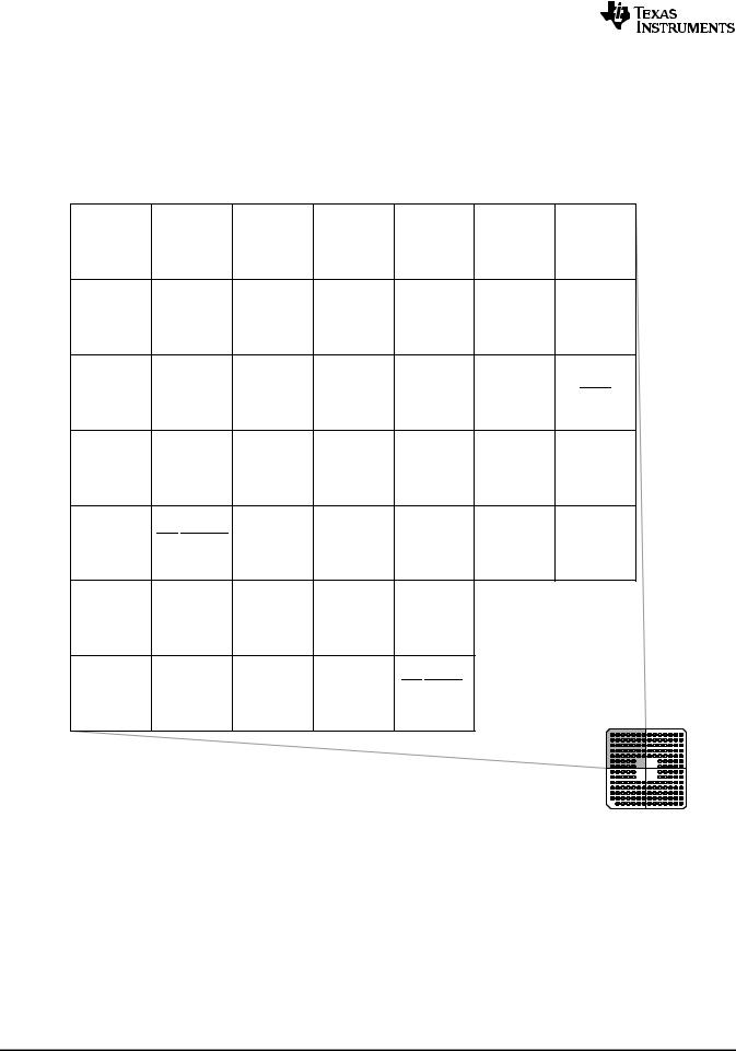
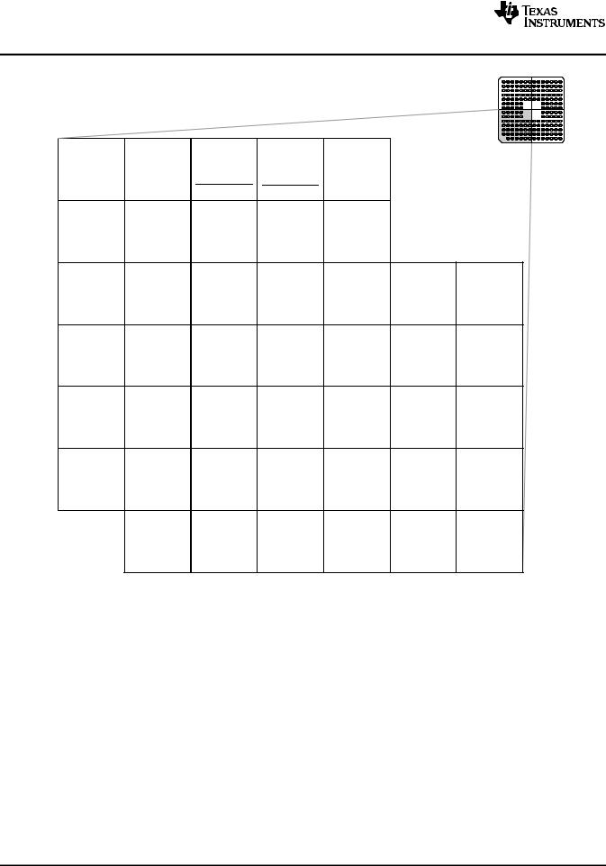
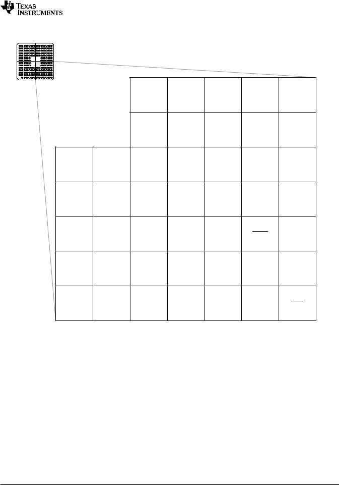
The 179-ball ZHH ball grid array (BGA) terminal assignments are shown in Figure 2-1 through Figure 2-4. The 256-ball ZFE plastic ball grid array (PBGA) terminal assignments are shown in Figure 2-5 through Figure 2-8. Table 2-2 describes the function(s) of each pin.
|
1 |
2 |
3 |
4 |
5 |
6 |
7 |
|
|
|
|
|
GPIO19/ |
GPIO23/ |
GPIO24/ |
GPIO32/ |
|
|
|
P |
EXTSOC2B |
EXTSOC3B |
SPISTEA/ |
EQEP1I/ |
ECAP1/ |
SDAA/ |
VDD |
P |
|
SCIRXDB/ |
MFSXA/ |
EQEP2A/ |
EPWMSYNCI/ |
||||||
|
|
|
CANTXA |
SCIRXDB |
MDXB |
ADCSOCAO |
|
|
|
|
|
|
|
GPIO22/ |
|
GPIO33/ |
|
|
|
|
|
|
|
|
|
|
|
||
N |
EXTSOC1A |
EXTSOC3A |
EXTADCCLK |
EQEP1S/ |
VDD |
SCLA/ |
TDO |
N |
|
MCLKXA/ |
|||||||||
|
|
|
|
|
EPWMSYNCO/ |
|
|
||
|
|
|
|
|
|
|
|
||
|
|
|
|
SCITXDB |
|
ADCSOCBO |
|
|
|
|
|
|
|
|
|
|
|
||
|
|
|
|
GPIO21/ |
GPIO25/ |
GPIO27/ |
|
|
|
M |
VDD |
EXTSOC2A |
EXTSOC1B |
EQEP1B/ |
ECAP2/ |
ECAP4/ |
TRST |
M |
|
MDRA/ |
EQEP2B/ |
EQEP2S/ |
|||||||
|
|
|
|
CANRXB |
MDRB |
MFSXB |
|
|
|
|
GPIO18/ |
|
|
GPIO20/ |
|
|
|
|
|
L |
SPICLKA/ |
VDDIO |
VSS |
EQEP1A/ |
VSS |
TDI |
VSS |
L |
|
SCITXDB/ |
MDXA/ |
||||||||
|
CANRXA |
|
|
CANTXB |
|
|
|
|
|
|
|
GPIO15/ |
|
GPIO16/ |
|
GPIO26/ |
|
|
|
K |
VSS |
TZ4/XHOLDA/ |
VDD |
SPISIMOA/ |
VDDIO |
ECAP3/ |
VDDIO |
K |
|
SCIRXDB/ |
CANTXB/ |
EQEP2I/ |
|||||||
|
|
MFSXB |
|
TZ5 |
|
MCLKXB |
|
|
|
|
|
|
|
|
GPIO17/ |
6 |
7 |
|
|
|
|
|
|
|
|
|
|
||
J |
VDDIO |
VSS |
VDD |
VDD |
SPISOMIA/ |
J |
|
|
|
CANRXB/ |
|
|
|||||||
|
|
|
|
|
TZ6 |
|
|
|
|
|
|
GPIO12/ |
GPIO11/ |
GPIO13/ |
GPIO14/ |
|
|
|
|
H |
VSS |
TZ1/ |
EPWM6B/ |
TZ2/ |
TZ3/XHOLD/ |
H |
|
|
|
CANTXB/ |
SCIRXDB/ |
CANRXB/ |
SCITXDB/ |
|
|
||||
|
|
MDXB |
ECAP4 |
MDRB |
MCLKXB |
|
|
|
|
|
1 |
2 |
3 |
4 |
5 |
|
|
|
Figure 2-1. C2834x 179-Ball ZHH MicroStar BGA™ Upper Left Quadrant (Bottom VIew)
16 |
Introduction |
Copyright © 2009–2010, Texas Instruments Incorporated |
Submit Documentation Feedback
Product Folder Link(s): TMS320C28346, TMS320C28345, TMS320C28344 TMS320C28343, TMS320C28342,
TMS320C28341

TMS320C28346, TMS320C28345, TMS320C28344
TMS320C28343, TMS320C28342, TMS320C28341
www.ti.com SPRS516B –MARCH 2009 –REVISED JULY 2010
|
8 |
9 |
10 |
11 |
12 |
13 |
14 |
|
|
|
|
|
GPIO49/ |
|
GPIO54/ |
GPIO56/ |
GPIO58/ |
|
|
P |
XRS |
TCK |
ECAP6/ |
VDDIO |
SPISIMOA/ |
SPICLKA/ |
MCLKRA/ |
P |
|
XD30/ |
XD25/ |
XD23/ |
XD21/ |
||||||
|
|
|
SPISOMID |
|
EQEP3A |
EQEP3S |
EPWM7A |
|
|
|
|
|
GPIO50/ |
GPIO51/ |
GPIO55/ |
GPIO57/ |
|
|
|
|
|
|
EQEP1A/ |
EQEP1B/ |
SPISOMIA/ |
SPISTEA/ |
|
|
|
N |
XRSIO |
EMU0 |
XD29/ |
XD28/ |
XD24/ |
XD22/ |
VDD |
N |
|
|
|
|
SPICLKD |
SPISTED |
EQEP3B |
EQEP3I |
|
|
|
|
|
|
GPIO48/ |
GPIO52/ |
|
GPIO59/ |
GPIO60/ |
|
|
|
|
|
ECAP5/ |
|
MFSRA/ |
MCLKRB/ |
|
||
M |
TMS |
VSS |
EQEP1S/ |
VSS |
M |
||||
XD31/ |
XD20/ |
XD19/ |
|||||||
|
|
|
XD27 |
|
|
||||
|
|
|
SPISIMOD |
|
EPWM7B |
EPWM8A |
|
||
|
|
|
|
|
|
||||
|
|
|
|
GPIO53/ |
GPIO61/ |
GPIO62/ |
|
|
|
|
VSS |
|
VDD |
MFSRB/ |
SCIRXDC/ |
VDDIO |
|
||
L |
EMU1 |
EQEP1I/ |
L |
||||||
|
|
|
|
XD18/ |
XD17/ |
|
|
||
|
|
|
|
XD26 |
|
|
|||
|
|
|
|
EPWM8B |
EPWM9A |
|
|
||
|
|
|
|
|
|
|
|||
|
|
|
|
|
|
GPIO63/ |
|
|
|
K |
VDDIO |
VDD |
VSS |
VDD |
GPIO64/ |
SCITXDC/ |
GPIO65/ |
K |
|
XD15 |
XD16/ |
XD14 |
|||||||
|
|
|
|
|
|
EPWM9B |
|
|
|
|
8 |
9 |
|
|
|
|
|
|
|
|
|
J |
VSS |
GPIO66/ |
GPIO67/ |
GPIO68/ |
VDDIO |
J |
|
|
|
XD13 |
XD12 |
XD11 |
|||||
|
|
|
VSS |
VDD |
GPIO70/ |
GPIO69/ |
VDD |
|
|
|
|
H |
XD9 |
XD10 |
H |
||||
|
|
|
10 |
11 |
12 |
13 |
14 |
|
Figure 2-2. C2834x 179-Ball ZHH MicroStar BGA™ Upper Right Quadrant (Bottom View)
Copyright © 2009–2010, Texas Instruments Incorporated |
Introduction |
17 |
Submit Documentation Feedback
Product Folder Link(s): TMS320C28346, TMS320C28345, TMS320C28344 TMS320C28343, TMS320C28342,
TMS320C28341
TMS320C28346, TMS320C28345, TMS320C28344 |
|
|
|
|
|||||
TMS320C28343, TMS320C28342, TMS320C28341 |
|
|
|
|
|||||
SPRS516B –MARCH 2009 –REVISED JULY 2010 |
|
|
|
|
|
www.ti.com |
|||
|
1 |
2 |
3 |
4 |
5 |
|
|
|
|
|
|
GPIO9/ |
GPIO10/ |
GPIO8/ |
|
|
|
|
|
G |
VDD |
EPWM5B/ |
EPWM6A/ |
EPWM5A/ |
VSS |
G |
|
|
|
|
SCITXDB/ |
CANRXB/ |
CANTXB/ |
|
|
|
|||
|
|
|
|
|
|
||||
|
|
ECAP3 |
ADCSOCBO |
ADCSOCAO |
|
|
|
|
|
|
|
GPIO7/ |
GPIO6/ |
|
|
|
|
|
|
F |
VDDIO |
EPWM4B/ |
EPWM4A/ |
VSS |
GPIO2/ |
F |
|
|
|
MCLKRA/ |
EPWMSYNCI/ |
EPWM2A |
|
|
|||||
|
|
ECAP2 |
EPWMSYNCO |
|
|
6 |
7 |
|
|
|
|
|
GPIO5/ |
GPIO3/ |
|
|
|
|
|
E |
VDD |
GPIO4/ |
EPWM3B/ |
EPWM2B/ |
VDD |
GPIO80/ |
GPIO46/ |
E |
|
EPWM3A |
MFSRA/ |
ECAP5/ |
XA8 |
XA6 |
|||||
|
|
|
ECAP1 |
MCLKRB |
|
|
|
|
|
D |
VDD |
VSS |
VDDIO |
GPIO85/ |
GPIO84/ |
GPIO47/ |
VDDIO |
D |
|
XA13 |
XA12 |
XA7 |
|||||||
|
GPIO1/ |
GPIO30/ |
GPIO29/ |
|
|
|
|
|
|
|
EPWM1B/ |
VDD |
GPIO81/ |
VDD |
VDD18 |
|
|||
C |
CANRXA/ |
SCITXDA/ |
C |
||||||
ECAP6/ |
XA9 |
||||||||
|
XA18 |
XA19 |
|
|
|
|
|||
|
MFSRB |
|
|
|
|
|
|||
|
|
|
|
|
|
|
|
||
|
GPIO0/ |
GPIO31/ |
GPIO87/ |
VDDIO |
GPIO83/ |
VDDIO |
VDD |
|
|
B |
CANTXA/ |
B |
|||||||
EPWM1A |
XA15 |
|
XA11 |
|
|
||||
|
XA17 |
|
|
|
|
||||
|
|
|
|
|
|
|
|
||
A |
|
GPIO39/ |
GPIO86/ |
VSS |
GPIO82/ |
VSS |
VSS |
A |
|
|
XA16 |
XA14 |
XA10 |
||||||
|
1 |
2 |
3 |
4 |
5 |
6 |
7 |
|
|
|
Figure 2-3. C2834x 179-Ball ZHH MicroStar BGA™ |
Lower Left Quadrant (Bottom View) |
|||||||
18 |
Introduction |
Copyright © 2009–2010, Texas Instruments Incorporated |
Submit Documentation Feedback
Product Folder Link(s): TMS320C28346, TMS320C28345, TMS320C28344 TMS320C28343, TMS320C28342,
TMS320C28341
TMS320C28346, TMS320C28345, TMS320C28344
TMS320C28343, TMS320C28342, TMS320C28341
www.ti.com |
SPRS516B –MARCH 2009 –REVISED JULY 2010 |
|
|
|
|
|
|
|
|
10 |
11 |
12 |
13 |
14 |
|
|
|
|
G |
VDD |
VSS |
GPIO71/ |
GPIO72/ |
VSS |
G |
|
|
|
|
XD8 |
XD7 |
|
|||
|
|
|
F |
GPIO78/ |
VDDIO |
GPIO75/ |
GPIO74/ |
GPIO73/ |
F |
|
|
|
XD1 |
XD4 |
XD5 |
XD6 |
|||
|
8 |
9 |
|
|
|
|
|
|
|
E |
VDD18 |
VSS |
|
GPIO40/ |
GPIO77/ |
VDD |
GPIO76/ |
VSS |
E |
|
XA0 |
XD2 |
XD3 |
||||||
|
|
|
|
GPIO41/ |
GPIO37/ |
|
|
|
|
D |
VSS |
XCLKIN |
|
ECAP2/ |
VDD |
VSS |
VDDIO |
D |
|
|
XA1 |
||||||||
|
|
|
|
XZCS7 |
|
|
|
|
|
|
|
|
|
|
|
|
|
|
|
|
X1 |
VDDIO |
|
VDD |
VDD |
GPIO38/ |
XWE1 |
GPIO79/ |
|
C |
|
XWE0 |
XD0 |
C |
|||||
|
|
GPIO45/ |
|
GPIO42/ |
|
GPIO36/ |
GPIO35/ |
|
|
|
VSSK |
|
VSS |
SCIRXDA/ |
SCITXDA/ |
XCLKOUT |
|
||
B |
XA5 |
|
XA2 |
B |
|||||
|
|
|
|
XZCS0 |
XR/W |
|
|
||
|
|
|
|
|
|
|
|
||
A |
X2 |
GPIO44/ |
|
GPIO43/ |
|
GPIO28/ |
GPIO34/ |
|
A |
|
VDDIO |
SCIRXDA/ |
ECAP1 |
XRD |
|||||
|
|
XA4 |
|
XA3 |
|
||||
|
|
|
|
XZCS6 |
XREADY |
|
|
||
|
|
|
|
|
|
|
|
||
|
8 |
9 |
|
10 |
11 |
12 |
13 |
14 |
|
Figure 2-4. C2834x 179-Ball ZHH MicroStar BGA™ Lower Right Quadrant (Bottom View)
Copyright © 2009–2010, Texas Instruments Incorporated |
Introduction |
19 |
Submit Documentation Feedback
Product Folder Link(s): TMS320C28346, TMS320C28345, TMS320C28344 TMS320C28343, TMS320C28342,
TMS320C28341

TMS320C28346, TMS320C28345, TMS320C28344
TMS320C28343, TMS320C28342, TMS320C28341
SPRS516B –MARCH 2009 –REVISED JULY 2010 www.ti.com
1 2 3 4 5 6 7 8
|
|
|
|
|
GPIO19/ |
GPIO21/ |
GPIO24/ |
GPIO27/ |
|
|
|
|
T |
VSS |
VSS |
|
VDDIO |
SPISTEA/ |
EQEP1B/ |
ECAP1/ |
ECAP4/ |
TDI |
|
|
|
|
SCIRXDB/ |
MDRA/ |
EQEP2A/ |
EQEP2S/ |
|
|
|
|||||
|
|
|
|
|
CANTXA |
CANRXB |
MDXB |
MFSXB |
|
|
|
|
|
|
|
|
|
|
|
|
|
|
|
|
|
|
|
|
|
|
GPIO20/ |
GPIO22/ |
GPIO25/ |
GPIO32/ |
|
|
|
|
R |
VSS |
VSS |
|
EXTADCCLK |
EQEP1A/ |
EQEP1S/ |
ECAP2/ |
SDAA/ |
TRST |
|
|
|
|
MDXA/ |
MCLKXA/ |
EQEP2B/ |
EPWMSYNCI/ |
|
|
|
|||||
|
|
|
|
|
CANTXB |
SCITXDB |
MDRB |
ADCSOCAO |
|
|
|
|
|
|
|
|
|
|
|
|
|
|
|
|
|
|
|
|
|
|
|
GPIO23/ |
GPIO26/ |
GPIO33/ |
|
|
|
|
P |
VDD |
EXTSOC3B |
VSS |
VSS |
EQEP1I/ |
ECAP3/ |
SCLA/ |
TDO |
|
|
|
|
MFSXA/ |
EQEP2I/ |
EPWMSYNCO/ |
|
|
|
|||||||
|
|
|
|
|
|
SCIRXDB |
MCLKXB |
ADCSOCBO |
|
|
|
|
|
|
|
|
|
|
|
|
|
|
|
|
|
N |
EXTSOC2A |
EXTSOC2B |
EXTSOC3A |
VSS |
VDDIO |
VDDIO |
VSS |
VDDIO |
|
|
|
|
|
|
|
|
|
|
|
|
|
|
|
|
|
|
GPIO18/ |
|
|
|
|
|
|
|
|
|
|
|
M |
SPICLKA/ |
EXTSOC1A |
EXTSOC1B |
VDDIO |
VSS |
VDD |
VDD |
VDD |
|
|
|
|
SCITXDB/ |
|
|
|
|||||||||
|
CANRXA |
|
|
|
|
|
|
|
|
|
|
|
|
|
|
|
|
|
|
|
|
|
|
|
|
|
GPIO16/ |
GPIO17/ |
|
|
|
|
|
|
|
|
|
|
|
|
|
|
|
|
|
|
|
|
|
|
|
L |
SPISIMOA/ |
SPISOMIA/ |
VDD |
VDDIO |
VDD |
VSS |
VSS |
VSS |
|
|
|
|
|
|
|
|
|||||||||
CANTXB/ |
CANRXB/ |
|
|
|
|
|||||||
|
|
|
|
|
|
|
|
|
|
|
|
|
|
TZ5 |
TZ6 |
|
|
|
|
|
|
|
|
|
|
|
|
|
|
|
|
|
|
|
|
|
|
|
|
|
|
|
|
|
|
|
|
|
|
|
|
|
|
GPIO15/ |
|
|
|
|
|
|
|
|
|
|
K |
VSS |
TZ4/XHOLDA |
/ |
VDD |
VSS |
VDD |
VSS |
VSS |
VSS |
|
|
|
|
SCIRXDB/ |
|
|
|
|
|||||||
|
|
MFSXB |
|
|
|
|
|
|
|
|
|
|
|
|
|
|
|
|
|
|
|
|
|
|
|
|
|
GPIO13/ |
|
GPIO14/ |
|
|
|
|
|
|
|
|
J |
VDDIO |
TZ2/ |
|
TZ3/XHOLD/ |
VDDIO |
VDD |
VSS |
VSS |
VSS |
|
|
|
CANRXB/ |
|
SCITXDB/ |
|
|
|
|||||||
|
|
MDRB |
|
MCLKXB |
|
|
|
|
|
|
|
|
|
|
|
|
|
|
|
|
|
|
|
|
|
|
|
|
|
|
|
|
|
|
|
|
|
|
|
|
|
|
|
|
|
|
|
|
|
|
|
|
|
|
|
|
|
|
|
|
|
|
|
|
Figure 2-5. C2834x 256-Ball ZFE Plastic BGA Upper Left Quadrant (Bottom View)
20 |
Introduction |
Copyright © 2009–2010, Texas Instruments Incorporated |
Submit Documentation Feedback
Product Folder Link(s): TMS320C28346, TMS320C28345, TMS320C28344 TMS320C28343, TMS320C28342,
TMS320C28341
TMS320C28346, TMS320C28345, TMS320C28344
TMS320C28343, TMS320C28342, TMS320C28341
www.ti.com SPRS516B –MARCH 2009 –REVISED JULY 2010
|
|
|
9 |
|
10 |
|
11 |
12 |
|
13 |
14 |
15 |
16 |
|
|||
|
|
|
|
|
|
|
|
|
|
|
|
|
|
|
|
|
|
|
|
|
|
|
|
|
|
|
|
|
GPIO50/ |
GPIO53/ |
|
|
|
|
|
|
|
|
|
|
|
|
|
|
|
EQEP1A/ |
|
|
|
|
|||
|
|
|
|
|
|
|
|
|
TCK |
EQEP1I/ |
VDDIO |
VSS |
VSS |
T |
|||
|
|
|
XRSIO |
XRS |
|||||||||||||
|
|
|
|
XD29/ |
|||||||||||||
|
|
|
|
|
|
|
|
|
|
|
XD26 |
|
|
|
|
||
|
|
|
|
|
|
|
|
|
|
SPICLKD |
|
|
|
|
|||
|
|
|
|
|
|
|
|
|
|
|
|
|
|
|
|||
|
|
|
|
|
|
|
|
|
|
|
|
|
|
|
|
|
|
|
|
|
|
|
|
|
|
|
GPIO48/ |
|
GPIO51/ |
GPIO54/ |
GPIO56/ |
|
|
|
|
|
|
|
|
VDDIO |
EMU1 |
ECAP5/ |
EQEP1B/ |
SPISIMOA/ |
SPICLKA/ |
VSS |
VSS |
R |
|||||
|
|
|
|
XD31/ |
|
XD28/ |
XD25/ |
XD23/ |
|||||||||
|
|
|
|
|
|
|
|
|
|
|
|
|
EQEP3A |
EQEP3S |
|
|
|
|
|
|
|
|
|
|
|
|
SPISIMOD |
SPISTED |
|
|
|
||||
|
|
|
|
|
|
|
|
|
|
|
|
|
|
|
|
|
|
|
|
|
|
|
|
|
|
|
GPIO49/ |
|
GPIO52/ |
GPIO55/ |
|
GPIO57/ |
|
|
|
|
|
|
|
|
|
|
|
|
ECAP6/ |
|
SPISOMIA/ |
|
SPISTEA/ |
|
|
||
|
|
|
|
TMS |
EMU0 |
EQEP1S/ |
VSS |
VDD |
P |
||||||||
|
|
|
|
XD30/ |
XD24/ |
XD22/ |
|||||||||||
|
|
|
|
|
|
|
|
|
|
XD27 |
|
|
|
||||
|
|
|
|
|
|
|
|
|
SPISOMID |
|
EQEP3B |
|
EQEP3I |
|
|
||
|
|
|
|
|
|
|
|
|
|
|
|
|
|
|
|||
|
|
|
|
|
|
|
|
|
|
|
|
|
|
|
|
|
|
|
|
|
|
|
|
|
|
|
|
|
|
|
|
|
GPIO59/ |
GPIO58/ |
|
|
|
|
|
VSS |
|
VSS |
VDDIO |
|
VDDIO |
VSS |
VSS |
MFSRA/ |
MCLKRA/ |
N |
|||
|
|
|
|
|
|
XD20/ |
XD21/ |
||||||||||
|
|
|
|
|
|
|
|
|
|
|
|
|
|
|
EPWM7B |
EPWM7A |
|
|
|
|
|
|
|
|
|
|
|
|
|
|
|
|
|
|
|
|
|
|
|
|
|
|
|
|
|
|
|
|
|
GPIO62/ |
GPIO61/ |
GPIO60/ |
|
|
|
|
|
VDD |
|
VDD |
VDD |
|
VSS |
VDDIO |
SCIRXDC/ |
MFSRB/ |
MCLKRB/ |
M |
|||
|
|
|
|
|
|
XD17/ |
XD18/ |
XD19/ |
|||||||||
|
|
|
|
|
|
|
|
|
|
|
|
|
|
EPWM9A |
EPWM8B |
EPWM8A |
|
|
|
|
|
|
|
|
|
|
|
|
|
|
|
|
|
|
|
|
|
|
|
|
|
|
|
|
|
|
|
|
|
|
|
GPIO63/ |
|
|
|
|
|
VSS |
|
VSS |
VSS |
|
VDD |
VDDIO |
GPIO65/ |
GPIO64/ |
SCITXDC/ |
L |
|||
|
|
|
|
|
|
XD14 |
XD15 |
XD16/ |
|||||||||
|
|
|
|
|
|
|
|
|
|
|
|
|
|
|
|
EPWM9B |
|
|
|
|
|
|
|
|
|
|
|
|
|
|
|
|
|
|
|
|
|
|
|
VSS |
|
VSS |
VSS |
|
VDD |
VSS |
GPIO67/ |
GPIO66/ |
VSS |
K |
|||
|
|
|
|
|
|
XD12 |
XD13 |
||||||||||
|
|
|
|
|
|
|
|
|
|
|
|
|
|
|
|
|
|
|
|
|
|
VSS |
|
VSS |
VSS |
|
VDD |
VDDIO |
GPIO69/ |
GPIO68/ |
VDDIO |
J |
|||
|
|
|
|
|
|
XD10 |
XD11 |
||||||||||
|
|
|
|
|
|
|
|
|
|
|
|
|
|
|
|
|
|
|
|
|
|
|
|
|
|
|
|
|
|
|
|
|
|
|
|
|
|
|
|
|
|
|
|
|
|
|
|
|
|
|
|
|
|
|
|
|
|
|
|
|
|
|
|
|
|
|
|
|
|
|
|
Figure 2-6. C2834x 256-Ball ZFE Plastic BGA Upper Right Quadrant (Bottom View)
Copyright © 2009–2010, Texas Instruments Incorporated |
Introduction |
21 |
Submit Documentation Feedback
Product Folder Link(s): TMS320C28346, TMS320C28345, TMS320C28344 TMS320C28343, TMS320C28342,
TMS320C28341

TMS320C28346, TMS320C28345, TMS320C28344
TMS320C28343, TMS320C28342, TMS320C28341
SPRS516B –MARCH 2009 –REVISED JULY 2010 |
|
www.ti.com |
|
|
|
|
|
|
|
|
|
|
|
|
|
|
|
GPIO10/ |
|
GPIO11/ |
GPIO12/ |
|
|
|
|
|
|
H |
|
EPWM6A/ |
|
EPWM6B/ |
TZ1/ |
VSS |
VDD |
VSS |
VSS |
VSS |
|
|
CANRXB/ |
|
SCIRXDB/ |
CANTXB/ |
|||||||
|
|
|
|
|
|
|
|
|
|
|
|
|
ADCSOCBO |
|
ECAP4 |
MDXB |
|
|
|
|
|
||
|
|
|
|
|
|
|
|
|
|
|
|
|
|
GPIO7/ |
|
GPIO8/ |
GPIO9/ |
|
|
|
|
|
|
G |
|
EPWM4B/ |
|
EPWM5A/ |
EPWM5B/ |
VSS |
VDD |
VSS |
VSS |
VSS |
|
|
MCLKRA/ |
|
CANTXB/ |
SCITXDB/ |
|||||||
|
|
|
|
|
|
ECAP3 |
|
|
|
|
|
|
|
ECAP2 |
|
ADCSOCAO |
|
|
|
|
|
||
|
|
|
|
|
|
|
|
|
|
|
|
|
|
|
|
GPIO5/ |
GPIO6/ |
|
|
|
|
|
|
F |
|
GPIO4/ |
|
EPWM3B/ |
EPWM4A/ |
VDDIO |
VDD |
VSS |
VSS |
VSS |
|
|
EPWM3A |
|
MFSRA/ |
EPWMSYNCI/ |
|||||||
|
|
|
|
ECAP1 |
EPWMSYNCO |
|
|
|
|
|
|
|
|
|
|
|
|
|
|
|
|
|
|
|
|
GPIO1/ |
|
|
|
GPIO3/ |
|
|
|
|
|
E |
|
EPWM1B/ |
|
GPIO2/ |
EPWM2B/ |
VDDIO |
VSS |
VDD |
VDD |
VDD |
|
|
ECAP6/ |
|
EPWM2A |
ECAP5/ |
|||||||
|
|
MFSRB |
|
|
|
MCLKRB |
|
|
|
|
|
|
|
|
|
|
|
|
|
|
|
|
|
|
|
GPIO29/ |
|
GPIO0/ |
|
|
|
|
|
|
|
D |
|
SCITXDA/ |
|
VSS |
VSS |
VDDIO |
VDDIO |
VSS |
VDDIO |
||
|
|
EPWM1A |
|||||||||
|
|
XA19 |
|
|
|
|
|
|
|
||
|
|
|
|
|
|
|
|
|
|
|
|
|
|
|
|
|
|
|
|
|
|
|
|
|
|
|
|
GPIO30/ |
|
|
GPIO86/ |
GPIO83/ |
GPIO81/ |
GPIO47/ |
|
C |
|
VDD |
|
CANRXA/ |
VSS |
VSS |
|||||
|
|
XA14 |
XA11 |
XA9 |
XA7 |
||||||
|
|
|
|
XA18 |
|
|
|||||
|
|
|
|
|
|
|
|
|
|
||
|
|
|
|
|
|
|
|
|
|
|
|
|
|
|
|
|
|
GPIO31/ |
GPIO39/ |
GPIO85/ |
GPIO82/ |
GPIO80/ |
GPIO46/ |
B |
|
VSS |
|
VSS |
CANTXA/ |
||||||
|
|
XA16 |
XA13 |
XA10 |
XA8 |
XA6 |
|||||
|
|
|
|
|
|
XA17 |
|||||
|
|
|
|
|
|
|
|
|
|
|
|
|
|
|
|
|
|
|
|
|
|
|
|
A |
|
VSS |
|
VSS |
VDDIO |
GPIO87/ |
GPIO84/ |
VDD18 |
|
VSSK |
|
|
|
XA15 |
XA12 |
X1 |
|||||||
|
|
|
|
|
|
|
|
|
|
|
|
|
1 |
2 |
|
3 |
4 |
5 |
6 |
7 |
8 |
||
Figure 2-7. C2834x 256-Ball ZFE Plastic BGA Lower Left Quadrant (Bottom View)
22 |
Introduction |
Copyright © 2009–2010, Texas Instruments Incorporated |
Submit Documentation Feedback
Product Folder Link(s): TMS320C28346, TMS320C28345, TMS320C28344 TMS320C28343, TMS320C28342,
TMS320C28341

TMS320C28346, TMS320C28345, TMS320C28344
TMS320C28343, TMS320C28342, TMS320C28341
www.ti.com |
|
SPRS516B –MARCH 2009 –REVISED JULY 2010 |
|
|
|
|
|
|
|
|
|
|
|
|
|
VSS |
VSS |
VSS |
VDD |
VSS |
GPIO72/ |
GPIO71/ |
GPIO70/ |
||||||||||
|
XD7 |
|
XD8 |
XD9 |
|||||||||||||
|
|
|
|
|
|
|
|
|
|
|
|
|
|
|
|||
VSS |
V |
V |
|
V |
|
V |
|
GPIO75/ |
GPIO74/ |
GPIO73/ |
|||||||
SS |
DD |
SS |
|
|
|
|
|
|
|
|
|
|
|||||
|
SS |
|
|
|
|
XD4 |
|
XD5 |
XD6 |
||||||||
|
|
|
|
|
|
|
|
|
|
||||||||
|
|
|
|
|
|
|
|
|
|
|
|
|
|
|
|||
|
VSS |
VSS |
VDD |
VDDIO |
GPIO78/ |
GPIO77/ |
GPIO76/ |
||||||||||
VSS |
|
XD1 |
|
XD2 |
XD3 |
||||||||||||
|
|
|
|
|
|
|
|
|
|||||||||
|
|
|
|
|
|
|
|
|
|
|
|
|
|
|
|
||
VDD |
VDD |
VDD |
VSS |
VDDIO |
|
|
|
|
GPIO38/ |
GPIO79/ |
|||||||
XWE1 |
XWE0 |
XD0 |
|||||||||||||||
|
|
|
|
|
|
|
|
|
|
|
|
||||||
VSS |
VSS |
VDDIO |
VDDIO |
VSS |
|
VSS |
|
|
|
XCLKOUT |
|||||||
XRD |
|||||||||||||||||
|
|
|
|
|
|
|
|
|
|
|
|
|
|
|
|
|
|
GPIO45/ |
GPIO44/ |
GPIO42/ |
GPIO40/ |
|
|
|
|
|
|
GPIO35/ |
|
|
|||||
VSS |
|
VSS |
SCITXDA/ |
VDD |
|||||||||||||
XA5 |
XA4 |
XA2 |
XA0 |
|
|||||||||||||
|
|
|
|
|
|
XR/W |
|
|
|||||||||
|
|
|
|
|
|
|
|
|
|
|
|
|
|
||||
|
|
|
|
|
|
|
|
|
|
|
|
|
|
|
|||
|
GPIO43/ |
GPIO41/ |
GPIO37/ |
GPIO28/ |
GPIO34/ |
|
|
|
|
|
|
||||||
VDDIO |
ECAP2/ |
SCIRXDA/ |
ECAP1/ |
|
VSS |
VSS |
|||||||||||
XA3 |
XA1 |
|
|||||||||||||||
|
XZCS7 |
XZCS6 |
XREADY |
|
|
|
|
|
|
||||||||
|
|
|
|
|
|
|
|
|
|
||||||||
|
|
|
|
|
|
|
|
|
|
|
|
|
|
|
|
|
|
|
|
|
|
|
|
GPIO36/ |
|
|
|
|
|
|
|
|
|
|
|
X2 |
V |
VDD18 |
XCLKIN |
SCIRXDA/ |
|
V |
DDIO |
|
V |
SS |
V |
SS |
|||||
SS |
|
|
|
|
|
|
|
||||||||||
|
|
|
|
|
|
XZCS0 |
|
|
|
|
|
|
|
|
|
|
|
|
|
|
|
|
|
|
|
|
|
|
|
||||||
9 |
10 |
11 |
12 |
13 |
14 |
|
15 |
|
16 |
||||||||
Figure 2-8. C2834x 256-Ball ZFE Plastic BGA Lower Right Quadrant (Bottom View)
H
G
F
E
D
C
B
A
Copyright © 2009–2010, Texas Instruments Incorporated |
Introduction |
23 |
Submit Documentation Feedback
Product Folder Link(s): TMS320C28346, TMS320C28345, TMS320C28344 TMS320C28343, TMS320C28342,
TMS320C28341

TMS320C28346, TMS320C28345, TMS320C28344
TMS320C28343, TMS320C28342, TMS320C28341
SPRS516B –MARCH 2009 –REVISED JULY 2010 |
www.ti.com |
2.2Signal Descriptions
Table 2-2 describes the signals. The GPIO function (shown in Italics) is the default at reset. The peripheral signals that are listed under them are alternate functions. Some peripheral functions may not be available in all devices. See Table 2-1 for details. Inputs are not 5-V tolerant. All XINTF pins have a drive strength of 4 mA (typical). All GPIO pins are I/O/Z, 4-mA drive typical and have an internal pullup, which can be selectively enabled/disabled on a per-pin basis. This feature only applies to the GPIO pins. The pullups on GPIO0–GPIO11 and GPIO58–GPIO63 pins are not enabled at reset. The pullups on GPIO12–GPIO57 and GPIO64–GPIO87 are enabled upon reset.
|
|
|
|
|
|
Table 2-2. Signal Descriptions |
||||
|
|
|
|
|
|
|
|
|
|
|
|
NAME |
ZHH |
ZFE |
|
|
|
DESCRIPTION |
|||
|
BALL # |
BALL # |
|
|
|
|||||
|
|
|
|
|
|
|
|
|
||
|
|
|
|
|
|
|
JTAG |
|||
|
|
|
|
|
|
|
|
|
|
|
|
|
|
|
M7 |
R8 |
JTAG test reset with internal pulldown. |
TRST, |
when driven high, gives the scan system control of |
||
|
|
|
|
|
|
the operations of the device. If this signal is not connected or driven low, the device operates in its |
||||
|
|
|
|
|
|
functional mode, and the test reset signals are ignored. |
||||
|
|
|
|
|
|
NOTE: TRST is an active high test pin and must be maintained low at all times during normal |
||||
|
TRST |
|
|
|
||||||
|
|
|
|
device operation. An external pulldown resistor is recommended on this pin. The value of this |
||||||
|
|
|
|
|
|
|||||
|
|
|
|
|
|
resistor should be based on drive strength of the debugger pods applicable to the design. A 2.2-kΩ |
||||
|
|
|
|
|
|
resistor generally offers adequate protection. Since this is application-specific, it is recommended |
||||
|
|
|
|
|
|
that each target board be validated for proper operation of the debugger and the application. (I, ↓) |
||||
|
TCK |
|
P9 |
T11 |
JTAG test clock. An external pullup resistor is required on this pin. A 2.2-kΩ resistor generally offers |
|||||
|
|
|
|
adequate protection.(I) |
||||||
|
|
|
|
|
|
|||||
|
TMS |
|
M8 |
P9 |
JTAG test-mode select (TMS) with internal pullup. This serial control input is clocked into the TAP |
|||||
|
|
|
|
controller on the rising edge of TCK. (I, ↑) |
||||||
|
|
|
|
|
|
|||||
|
TDI |
|
L6 |
T8 |
JTAG test data input (TDI) with internal pullup. TDI is clocked into the selected register (instruction |
|||||
|
|
|
|
or data) on a rising edge of TCK. (I, ↑) |
||||||
|
|
|
|
|
|
|||||
|
TDO |
|
N7 |
P8 |
JTAG scan out, test data output (TDO). The contents of the selected register (instruction or data) |
|||||
|
|
|
|
are shifted out of TDO on the falling edge of TCK. |
||||||
|
|
|
|
|
|
|||||
|
|
|
|
|
|
|
|
|
|
|
|
|
|
|
N9 |
P10 |
Emulator pin 0. When |
|
is driven high, this pin is used as an interrupt to or from the emulator |
||
|
|
|
|
TRST |
||||||
|
|
|
|
|
|
system and is defined as input/output through the JTAG scan. This pin is also used to put the |
||||
|
|
|
|
|
|
device into boundary-scan mode. With the EMU0 pin at a logic-high state and the EMU1 pin at a |
||||
|
EMU0 |
|
|
|
logic-low state, a rising edge on the TRST pin would latch the device into boundary-scan mode. |
|||||
|
|
|
|
NOTE: An external pullup resistor is recommended on this pin. The value of this resistor should be |
||||||
|
|
|
|
|
|
|||||
|
|
|
|
|
|
based on the drive strength of the debugger pods applicable to the design. A 2.2-kΩ to 4.7-kΩ |
||||
|
|
|
|
|
|
resistor is generally adequate. Since this is application-specific, it is recommended that each target |
||||
|
|
|
|
|
|
board be validated for proper operation of the debugger and the application. |
||||
|
|
|
|
|
|
|
|
|
|
|
|
|
|
|
L9 |
R10 |
Emulator pin 1. When |
|
is driven high, this pin is used as an interrupt to or from the emulator |
||
|
|
|
|
TRST |
||||||
|
|
|
|
|
|
system and is defined as input/output through the JTAG scan. This pin is also used to put the |
||||
|
|
|
|
|
|
device into boundary-scan mode. With the EMU0 pin at a logic-high state and the EMU1 pin at a |
||||
|
EMU1 |
|
|
|
logic-low state, a rising edge on the TRST pin would latch the device into boundary-scan mode. |
|||||
|
|
|
|
NOTE: An external pullup resistor is recommended on this pin. The value of this resistor should be |
||||||
|
|
|
|
|
|
|||||
|
|
|
|
|
|
based on the drive strength of the debugger pods applicable to the design. A 2.2-kΩ to 4.7-kΩ |
||||
|
|
|
|
|
|
resistor is generally adequate. Since this is application-specific, it is recommended that each target |
||||
|
|
|
|
|
|
board be validated for proper operation of the debugger and the application. |
||||
|
|
|
|
|
|
|
|
|
|
|
|
|
|
|
|
|
|
Clock |
|||
|
|
|
|
|
|
|
|
|
|
|
|
|
|
|
B14 |
D16 |
Output clock derived from SYSCLKOUT. XCLKOUT is either the same frequency, one-half the |
||||
|
|
|
|
|
|
frequency, one-fourth the frequency, or one-eighth the frequency of SYSCLKOUT. This is controlled |
||||
|
XCLKOUT |
|
|
by bit 19 (BY4CLKMODE), bits 18:16 (XTIMCLK), and bit 2 (CLKMODE) in the XINTCNF2 register. |
||||||
|
|
|
At reset, XCLKOUT = SYSCLKOUT/8. The XCLKOUT signal can be turned off by setting |
|||||||
|
|
|
|
|
|
|||||
|
|
|
|
|
|
XINTCNF2[CLKOFF] to 1. Unlike other GPIO pins, the XCLKOUT pin is not placed in |
||||
|
|
|
|
|
|
high-impedance state during a reset. |
||||
|
|
|
|
D9 |
A12 |
External Oscillator Input. This pin is to feed a clock from an external 3.3-V oscillator. In this case, |
||||
|
XCLKIN |
|
|
the X1 pin must be tied to VSSK. If a crystal/resonator is used (or if an external 1.8-V oscillator is |
||||||
|
|
|
|
|
|
used to feed clock to X1 pin), this pin must be tied to VSS. (I) |
||||
|
|
|
|
C8 |
A7 |
Internal/External Oscillator Input. To use the internal oscillator, a quartz crystal may be connected |
||||
|
X1 |
|
|
|
across X1 and X2. The X1 pin is referenced to the 1.8-V core digital power supply. A 1.8-V external |
|||||
|
|
|
|
oscillator may be connected to the X1 pin. In this case, the XCLKIN pin must be connected to VSS. |
||||||
|
|
|
|
|
|
|||||
|
|
|
|
|
|
If a 3.3-V external oscillator is used with the XCLKIN pin, X1 must be tied to VSSK. (I) |
||||
|
X2 |
|
A8 |
A9 |
Internal Oscillator Output. A quartz crystal may be connected across X1 and X2. If X2 is not used it |
|||||
|
|
|
|
must be left unconnected. (O) |
||||||
|
|
|
|
|
|
|||||
|
|
|
|
|
|
|
|
|
|
|
|
|
|
|
|
|
|
|
|
|
|
24 |
|
Introduction |
|
|
|
|
|
Copyright © 2009–2010, Texas Instruments Incorporated |
||
Submit Documentation Feedback
Product Folder Link(s): TMS320C28346, TMS320C28345, TMS320C28344 TMS320C28343, TMS320C28342,
TMS320C28341

|
TMS320C28346, TMS320C28345, TMS320C28344 |
|
TMS320C28343, TMS320C28342, TMS320C28341 |
www.ti.com |
SPRS516B –MARCH 2009 –REVISED JULY 2010 |
|
|
|
|
|
|
Table 2-2. Signal Descriptions (continued) |
|
||||||||
|
|
NAME |
ZHH |
ZFE |
|
|
|
|
|
DESCRIPTION |
|
||||
|
|
BALL # |
BALL # |
|
|
|
|
|
|
||||||
|
|
|
|
|
|
|
|
|
|
|
|
|
|
||
|
|
|
|
|
|
|
|
|
|
|
|
||||
|
|
|
|
|
|
|
|
|
|
Reset |
|
||||
|
|
|
|
|
|
|
|
|
|
|
|
|
|
|
|
|
|
|
|
|
|
Device Reset (in) and Watchdog Reset (out). |
|
||||||||
|
|
|
|
|
|
Device reset. |
XRS |
causes the device to terminate execution. The PC will point to the address |
|
||||||
|
|
|
|
|
|
contained at the location 0x3FFFC0. When XRS is brought to a high level, execution begins at the |
|
||||||||
|
|
|
|
|
|
location pointed to by the PC. This pin is driven low by the MCU when a watchdog reset occurs. |
|
||||||||
|
XRS |
P8 |
T10 |
|
|
||||||||||
|
|
During watchdog reset, the XRS pin is driven low for the watchdog reset duration of 512 OSCCLK |
|
||||||||||||
|
|
|
|
|
|
|
|||||||||
|
|
|
|
|
|
cycles. (I/OD, ↑) |
|
|
|
|
|
|
|||
|
|
|
|
|
|
The output buffer of this pin is an open-drain with an internal pullup. It is recommended that this pin |
|||||||||
|
|
|
|
|
|
be driven by an open-drain device. |
|
||||||||
|
|
|
|
|
|
|
|
|
|
|
|
|
|
|
|
|
|
|
|
|
|
|
I/O Control (I) - |
This pin must be connected to the |
|
pin on the target board. When |
|
is |
|||
|
|
|
|
|
|
XRS |
XRS |
XRS |
|||||||
|
XRSIO |
N8 |
T9 |
|
low (reset), the level detected on this pin puts all output buffers on the device in high-impedance |
|
|||||||||
|
|
|
|
|
|
mode. |
|
|
|
|
|
|
|||
|
|
|
|
|
|
|
|
|
|
|
|
|
|
|
|
|
|
|
|
|
|
|
External ADC Interface Signals |
|
|||||||
|
|
|
|
|
|
|
|
|
|
|
|
|
|
|
|
|
EXTSOC1A |
N1 |
M2 |
|
External ADC SOC Group 1 A Output. Trigger for external ADC, this signal is logical OR of |
|
|||||||||
|
|
|
|
|
|
ePWM1/2/3 SOCA internal signals (O) |
|
||||||||
|
|
|
|
|
|
|
|
|
|
|
|
|
|
|
|
|
EXTSOC1B |
M3 |
M3 |
|
External ADC SOC Group 1 B Output. Trigger for external ADC, this signal is logical OR of |
|
|||||||||
|
|
|
|
|
|
ePWM1/2/3 SOCB internal signals (O) |
|
||||||||
|
EXTSOC2A |
M2 |
N1 |
|
External ADC SOC Group 2 A Output. Trigger for external ADC, this signal is logical OR of |
|
|||||||||
|
|
|
|
|
|
ePWM4/5/6 SOCA internal signals (O) |
|
||||||||
|
|
|
|
|
|
|
|
|
|
|
|
|
|
|
|
|
EXTSOC2B |
P1 |
N2 |
|
External ADC SOC Group 2 B Output. Trigger for external ADC, this signal is logical OR of |
|
|||||||||
|
|
|
|
|
|
ePWM4/5/6 SOCB internal signals (O) |
|
||||||||
|
|
|
|
|
|
|
|
|
|
|
|
|
|
|
|
|
EXTSOC3A |
N2 |
N3 |
|
External ADC SOC Group 3 A Output. Trigger for external ADC, this signal is logical OR of |
|
|||||||||
|
|
|
|
|
|
ePWM7/8/9 SOCA internal signals (O) |
|
||||||||
|
|
|
|
|
|
|
|
|
|
|
|
|
|
|
|
|
EXTSOC3B |
P2 |
P2 |
|
External ADC SOC Group3 B Output. Trigger for external ADC, this signal is logical OR of |
|
|||||||||
|
|
|
|
|
|
ePWM7/8/9 SOCB internal signals (O) |
|
||||||||
|
|
|
|
|
|
|
|
|
|
|
|
|
|
|
|
|
EXTADCCLK |
N3 |
R3 |
|
External ADC Clock Signal. Clock for external ADC support, derived from SYSCLK (O) |
|
|||||||||
|
|
|
|
|
|
|
|
|
|
|
|
|
|
|
|
|
|
|
|
|
|
|
|
GPIO and Peripheral Signals |
|
||||||
|
|
|
|
|
|
|
|
|
|
|
|
|
|
|
|
|
GPIO0 |
|
|
|
General purpose input/output 0 (I/O/Z) |
|
|||||||||
|
EPWM1A |
B1 |
D2 |
|
Enhanced PWM1 Output A and HRPWM channel (O) |
|
|||||||||
- |
|
- |
|
|
|
|
|
|
|
|
|
||||
|
|
|
|
|
|
|
|
|
|
|
|
||||
- |
|
|
|
- |
|
|
|
|
|
|
|
|
|
||
|
|
|
|
|
|
|
|
|
|
|
|
|
|
|
|
|
GPIO1 |
|
|
|
General purpose input/output 1 (I/O/Z) |
|
|||||||||
|
EPWM1B |
C1 |
E1 |
|
Enhanced PWM1 Output B (O) |
|
|||||||||
|
ECAP6 |
|
Enhanced Capture 6 input/output (I/O) |
|
|||||||||||
|
|
|
|
|
|||||||||||
|
MFSRB |
|
|
|
McBSP-B receive frame synch (I/O) |
|
|||||||||
|
|
|
|
|
|
|
|
|
|
|
|
|
|
|
|
|
GPIO2 |
|
|
|
General purpose input/output 2 (I/O/Z) |
|
|||||||||
|
EPWM2A |
F5 |
E2 |
|
Enhanced PWM2 Output A and HRPWM channel (O) |
|
|||||||||
- |
|
- |
|
|
|
|
|
|
|
|
|
||||
|
|
|
|
|
|
|
|
|
|
|
|
||||
- |
|
|
|
- |
|
|
|
|
|
|
|
|
|
||
|
|
|
|
|
|
|
|
|
|
|
|
|
|
|
|
|
GPIO3 |
|
|
|
General purpose input/output 3 (I/O/Z) |
|
|||||||||
|
EPWM2B |
E4 |
E3 |
|
Enhanced PWM2 Output B (O) |
|
|||||||||
|
ECAP5 |
|
Enhanced Capture 5 input/output (I/O) |
|
|||||||||||
|
|
|
|
|
|||||||||||
|
MCLKRB |
|
|
|
McBSP-B receive clock (I/O) |
|
|||||||||
|
|
|
|
|
|
|
|
|
|
|
|
|
|
|
|
|
GPIO4 |
|
|
|
General purpose input/output 4 (I/O/Z) |
|
|||||||||
|
EPWM3A |
E2 |
F1 |
|
Enhanced PWM3 output A and HRPWM channel (O) |
|
|||||||||
- |
|
- |
|
|
|
|
|
|
|
|
|
||||
|
|
|
|
|
|
|
|
|
|
|
|
||||
- |
|
|
|
- |
|
|
|
|
|
|
|
|
|
||
|
|
|
|
|
|
|
|
|
|
|
|
|
|
|
|
|
GPIO5 |
|
|
|
General purpose input/output 5 (I/O/Z) |
|
|||||||||
|
EPWM3B |
E3 |
F2 |
|
Enhanced PWM3 output B (O) |
|
|||||||||
|
MFSRA |
|
McBSP-A receive frame synch (I/O) |
|
|||||||||||
|
|
|
|
|
|||||||||||
|
ECAP1 |
|
|
|
Enhanced Capture input/output 1 (I/O) |
|
|||||||||
|
|
|
|
|
|
|
|
|
|
|
|
|
|
|
|
|
GPIO6 |
|
|
|
General purpose input/output 6 (I/O/Z) |
|
|||||||||
|
EPWM4A |
F3 |
F3 |
|
Enhanced PWM4 output A and HRPWM channel (O) |
|
|||||||||
|
EPWMSYNCI |
|
External ePWM sync pulse input (I) |
|
|||||||||||
|
|
|
|
|
|||||||||||
|
EPWMSYNCO |
|
|
|
External ePWM sync pulse output (O) |
|
|||||||||
|
|
|
|
|
|
|
|
|
|
|
|
|
|
|
|
|
GPIO7 |
|
|
|
General purpose input/output 7 (I/O/Z) |
|
|||||||||
|
EPWM4B |
F2 |
G1 |
|
Enhanced PWM4 output B (O) |
|
|||||||||
|
MCLKRA |
|
McBSP-A receive clock (I/O) |
|
|||||||||||
|
|
|
|
|
|||||||||||
|
ECAP2 |
|
|
|
Enhanced capture input/output 2 (I/O) |
|
|||||||||
|
|
|
|
|
|
|
|
|
|
|
|
|
|
|
|
|
|
|
|
|
|
|
|
|
|
|
|
|
|
|
|
Copyright © 2009–2010, Texas Instruments Incorporated |
|
|
Introduction |
25 |
|||||||||||
Submit Documentation Feedback
Product Folder Link(s): TMS320C28346, TMS320C28345, TMS320C28344 TMS320C28343, TMS320C28342,
TMS320C28341

TMS320C28346, TMS320C28345, TMS320C28344
TMS320C28343, TMS320C28342, TMS320C28341
SPRS516B –MARCH 2009 –REVISED JULY 2010 www.ti.com
|
|
|
|
|
|
|
|
|
|
|
Table 2-2. Signal Descriptions (continued) |
||||||
|
|
|
NAME |
ZHH |
ZFE |
|
DESCRIPTION |
||||||||||
|
|
|
BALL # |
BALL # |
|
||||||||||||
|
|
|
|
|
|
|
|
|
|
|
|
|
|
|
|
||
|
|
|
|
|
|
|
|
|
|
||||||||
|
GPIO8 |
|
|
|
|
|
|
|
General Purpose Input/Output 8 (I/O/Z) |
||||||||
|
EPWM5A |
G4 |
G2 |
Enhanced PWM5 output A and HRPWM channel (O) |
|||||||||||||
|
CANTXB |
Enhanced CAN-B transmit (O) |
|||||||||||||||
|
|
|
|||||||||||||||
|
ADCSOCAO |
|
|
|
ADC start-of-conversion A (O) |
||||||||||||
|
GPIO9 |
|
|
|
|
|
|
|
General purpose input/output 9 (I/O/Z) |
||||||||
|
EPWM5B |
G2 |
G3 |
Enhanced PWM5 output B (O) |
|||||||||||||
|
SCITXDB |
SCI-B transmit data(O) |
|||||||||||||||
|
|
|
|||||||||||||||
|
ECAP3 |
|
|
|
|
|
|
|
Enhanced capture input/output 3 (I/O) |
||||||||
|
|
|
|
|
|||||||||||||
|
GPIO10 |
|
|
General purpose input/output 10 (I/O/Z) |
|||||||||||||
|
EPWM6A |
G3 |
H1 |
Enhanced PWM6 output A and HRPWM channel (O) |
|||||||||||||
|
CANRXB |
Enhanced CAN-B receive (I) |
|||||||||||||||
|
|
|
|||||||||||||||
|
ADCSOCBO |
|
|
|
ADC start-of-conversion B (O) |
||||||||||||
|
GPIO11 |
|
|
General purpose input/output 11 (I/O/Z) |
|||||||||||||
|
EPWM6B |
H3 |
H2 |
Enhanced PWM6 output B (O) |
|||||||||||||
|
SCIRXDB |
SCI-B receive data (I) |
|||||||||||||||
|
|
|
|||||||||||||||
|
ECAP4 |
|
|
|
|
|
|
|
Enhanced CAP Input/Output 4 (I/O) |
||||||||
|
|
|
|
|
|
||||||||||||
|
GPIO12 |
|
|
General purpose input/output 12 (I/O/Z) |
|||||||||||||
|
TZ1 |
|
|
|
|
|
H2 |
H3 |
Trip Zone input 1 (I) |
||||||||
|
CANTXB |
Enhanced CAN-B transmit (O) |
|||||||||||||||
|
|
|
|||||||||||||||
|
MDXB |
|
|
|
|
|
|
|
McBSP-B transmit serial data (O) |
||||||||
|
|
|
|
|
|
||||||||||||
|
GPIO13 |
|
|
General purpose input/output 13 (I/O/Z) |
|||||||||||||
|
TZ2 |
|
|
|
|
|
H4 |
J2 |
Trip Zone input 2 (I) |
||||||||
|
CANRXB |
Enhanced CAN-B receive (I) |
|||||||||||||||
|
|
|
|||||||||||||||
|
MDRB |
|
|
|
|
|
|
|
McBSP-B receive serial data (I) |
||||||||
|
|
|
|
|
|
||||||||||||
|
GPIO14 |
|
|
General purpose input/output 14 (I/O/Z) |
|||||||||||||
|
|
|
|
|
|
|
|
|
|
|
Trip Zone input 3/External Hold Request. |
|
when active (low), requests the external interface |
||||
|
|
|
|
|
|
|
|
|
|
|
XHOLD, |
||||||
|
|
|
|
|
|
|
|
|
|
|
(XINTF) to release the external bus and place all buses and strobes into a high-impedance state. To |
||||||
|
|
|
|
|
|
|
|
|
|
|
prevent this from happening when TZ3 signal goes active, disable this function by writing |
|
|
||||
|
TZ3/XHOLD |
H5 |
J3 |
XINTCNF2[HOLD] = 1. If this is not done, the XINTF bus will go into high impedance anytime |
TZ3 |
|
|||||||||||
|
|
|
|
|
|
|
|
|
goes low. On the ePWM side, TZn signals are ignored by default, unless they are enabled by the |
||||||||
|
|
|
|
|
|
|
|
|
|
|
|||||||
|
|
|
|
|
|
|
|
|
|
|
code. The XINTF will release the bus when any current access is complete and there are no |
||||||
|
|
|
|
|
|
|
|
|
|
|
pending accesses on the XINTF. (I) |
||||||
|
SCITXDB |
|
|
SCI-B Transmit (O) |
|||||||||||||
|
MCLKXB |
|
|
McBSP-B transmit clock (I/O) |
|||||||||||||
|
|
|
|
|
|
|
|
|
|
|
|||||||
|
GPIO15 |
|
|
General purpose input/output 15 (I/O/Z) |
|||||||||||||
|
|
|
|
|
|
|
|
|
|
|
Trip Zone input 4/External Hold Acknowledge. The pin function for this option is based on the |
||||||
|
|
|
|
|
|
|
|
|
|
|
direction chosen in the GPADIR register. If the pin is configured as an input, then TZ4 function is |
||||||
|
|
|
|
|
|
|
|
|
|
|
chosen. If the pin is configured as an output, then |
XHOLDA |
function is chosen. XHOLDA is driven |
||||
|
TZ4/XHOLDA |
|
|
||||||||||||||
|
K2 |
K2 |
active (low) when the XINTF has granted an XHOLD request. All XINTF buses and strobe signals |
||||||||||||||
|
|
|
|
|
|
|
|
|
|||||||||
|
|
|
|
|
|
|
|
|
|
|
will be in a high-impedance state. XHOLDA is released when the XHOLD signal is released. |
||||||
|
|
|
|
|
|
|
|
|
|
|
External devices should only drive the external bus when XHOLDA is active (low). (I/O) |
||||||
|
SCIRXDB |
|
|
SCI-B receive (I) |
|||||||||||||
|
MFSXB |
|
|
McBSP-B transmit frame synch (I/O) |
|||||||||||||
|
|
|
|
|
|
|
|
|
|
|
|
|
|
|
|
||
|
GPIO16 |
|
|
General purpose input/output 16 (I/O/Z) |
|||||||||||||
|
SPISIMOA |
K4 |
L1 |
SPI slave in, master out (I/O) |
|||||||||||||
|
CANTXB |
Enhanced CAN-B transmit (O) |
|||||||||||||||
|
|
|
|||||||||||||||
|
TZ5 |
|
|
|
|
|
|
|
Trip Zone input 5 (I) |
||||||||
|
|
|
|
|
|
|
|
|
|
|
|
|
|
|
|
||
|
GPIO17 |
|
|
General purpose input/output 17 (I/O/Z) |
|||||||||||||
|
SPISOMIA |
J5 |
L2 |
SPI-A slave out, master in (I/O) |
|||||||||||||
|
CANRXB |
Enhanced CAN-B receive (I) |
|||||||||||||||
|
|
|
|||||||||||||||
|
TZ6 |
|
|
|
|
|
|
|
Trip zone input 6 (I) |
||||||||
|
|
|
|
|
|
|
|
|
|
|
|
|
|
|
|
||
|
GPIO18 |
|
|
General purpose input/output 18 (I/O/Z) |
|||||||||||||
|
SPICLKA |
L1 |
M1 |
SPI-A clock input/output (I/O) |
|||||||||||||
|
SCITXDB |
SCI-B transmit (O) |
|||||||||||||||
|
|
|
|||||||||||||||
|
CANRXA |
|
|
Enhanced CAN-A receive (I) |
|||||||||||||
|
|
|
|
|
|
|
|
|
|
|
|
|
|
|
|
||
|
GPIO19 |
|
|
General purpose input/output 19 (I/O/Z) |
|||||||||||||
|
SPISTEA |
|
|
|
|
P3 |
T4 |
SPI-A slave transmit enable input/output (I/O) |
|||||||||
|
SCIRXDB |
SCI-B receive (I) |
|||||||||||||||
|
|
|
|||||||||||||||
|
CANTXA |
|
|
Enhanced CAN-A transmit (O) |
|||||||||||||
|
|
|
|
|
|
|
|
|
|
|
|
|
|
|
|
|
|
|
|
|
|
|
|
|
|
|
|
|
|
|
|
|
|
|
|
26 |
|
|
Introduction |
|
|
|
|
Copyright © 2009–2010, Texas Instruments Incorporated |
|||||||||
Submit Documentation Feedback
Product Folder Link(s): TMS320C28346, TMS320C28345, TMS320C28344 TMS320C28343, TMS320C28342,
TMS320C28341

|
|
|
|
TMS320C28346, TMS320C28345, TMS320C28344 |
||
|
|
|
|
TMS320C28343, TMS320C28342, TMS320C28341 |
||
www.ti.com |
|
|
SPRS516B –MARCH 2009 –REVISED JULY 2010 |
|||
|
|
|
|
Table 2-2. Signal Descriptions (continued) |
|
|
|
|
|
|
|
|
|
NAME |
ZHH |
ZFE |
DESCRIPTION |
|
|
|
BALL # |
BALL # |
|
|
|||
|
|
|
|
|
||
|
|
|
|
|
|
|
GPIO20 |
|
|
|
General purpose input/output 20 (I/O/Z) |
|
|
EQEP1A |
|
L4 |
R4 |
Enhanced QEP1 input A (I) |
|
|
MDXA |
|
McBSP-A transmit serial data (O) |
|
|
||
|
|
|
|
|
||
CANTXB |
|
|
|
Enhanced CAN-B transmit (O) |
|
|
|
|
|
|
|
|
|
GPIO21 |
|
|
|
General purpose input/output 21 (I/O/Z) |
|
|
EQEP1B |
|
M4 |
T5 |
Enhanced QEP1 input B (I) |
|
|
MDRA |
|
McBSP-A receive serial data (I) |
|
|
||
|
|
|
|
|
||
CANRXB |
|
|
|
Enhanced CAN-B receive (I) |
|
|
|
|
|
|
|
|
|
GPIO22 |
|
|
|
General purpose input/output 22 (I/O/Z) |
|
|
EQEP1S |
|
N4 |
R5 |
Enhanced QEP1 strobe (I/O) |
|
|
MCLKXA |
|
McBSP-A transmit clock (I/O) |
|
|
||
|
|
|
|
|
||
SCITXDB |
|
|
|
SCI-B transmit (O) |
|
|
|
|
|
|
|
|
|
GPIO23 |
|
|
|
General purpose input/output 23 (I/O/Z) |
|
|
EQEP1I |
|
P4 |
P5 |
Enhanced QEP1 index (I/O) |
|
|
MFSXA |
|
McBSP-A transmit frame synch (I/O) |
|
|
||
|
|
|
|
|
||
SCIRXDB |
|
|
|
SCI-B receive (I) |
|
|
|
|
|
|
|
|
|
GPIO24 |
|
|
|
General purpose input/output 24 (I/O/Z) |
|
|
ECAP1 |
|
P5 |
T6 |
Enhanced capture 1 (I/O) |
|
|
EQEP2A |
|
Enhanced QEP2 input A (I) |
|
|
||
|
|
|
|
|
||
MDXB |
|
|
|
McBSP-B transmit serial data (O) |
|
|
|
|
|
|
|
|
|
GPIO25 |
|
|
|
General purpose input/output 25 (I/O/Z) |
|
|
ECAP2 |
|
M5 |
R6 |
Enhanced capture 2 (I/O) |
|
|
EQEP2B |
|
Enhanced QEP2 input B (I) |
|
|
||
|
|
|
|
|
||
MDRB |
|
|
|
McBSP-B receive serial data (I) |
|
|
|
|
|
|
|
|
|
GPIO26 |
|
|
|
General purpose input/output 26 (I/O/Z) |
|
|
ECAP3 |
|
K6 |
P6 |
Enhanced capture 3 (I/O) |
|
|
EQEP2I |
|
Enhanced QEP2 index (I/O) |
|
|
||
|
|
|
|
|
||
MCLKXB |
|
|
|
McBSP-B transmit clock (I/O) |
|
|
|
|
|
|
|
|
|
GPIO27 |
|
|
|
General purpose input/output 27 (I/O/Z) |
|
|
ECAP4 |
|
M6 |
T7 |
Enhanced capture 4 (I/O) |
|
|
EQEP2S |
|
Enhanced QEP2 strobe (I/O) |
|
|
||
|
|
|
|
|
||
MFSXB |
|
|
|
McBSP-B transmit frame synch (I/O) |
|
|
|
|
|
|
|
|
|
GPIO28 |
|
|
|
General purpose input/output 28 (I/O/Z) |
|
|
SCIRXDA |
|
A12 |
B13 |
SCI receive data (I) |
|
|
XZCS6 |
|
|
|
External Interface zone 6 chip select (O) |
|
|
|
|
|
|
|
|
|
GPIO29 |
|
|
|
General purpose input/output 29. (I/O/Z) |
|
|
SCITXDA |
|
C3 |
D1 |
SCI transmit data (O) |
|
|
XA19 |
|
|
|
External Interface Address Line 19 (O) |
|
|
|
|
|
|
|
|
|
GPIO30 |
|
|
|
General purpose input/output 30 (I/O/Z) |
|
|
CANRXA |
|
C2 |
C2 |
Enhanced CAN-A receive (I) |
|
|
XA18 |
|
|
|
External Interface Address Line 18 (O) |
|
|
GPIO31 |
|
|
|
General purpose input/output 31 (I/O/Z) |
|
|
CANTXA |
|
B2 |
B3 |
Enhanced CAN-A transmit (O) |
|
|
XA17 |
|
|
|
External Interface Address Line 17 (O) |
|
|
|
|
|
|
|
|
|
GPIO32 |
|
|
|
General purpose input/output 32 (I/O/Z) |
|
|
SDAA |
|
P6 |
R7 |
I2C data open-drain bidirectional port (I/OD) |
|
|
EPWMSYNCI |
Enhanced PWM external sync pulse input (I) |
|
|
|||
|
|
|
|
|||
ADCSOCAO |
|
|
ADC start-of-conversion A (O) |
|
|
|
|
|
|
|
|
|
|
GPIO33 |
|
|
|
General-Purpose Input/Output 33 (I/O/Z) |
|
|
SCLA |
|
N6 |
P7 |
I2C clock open-drain bidirectional port (I/OD) |
|
|
EPWMSYNCO |
Enhanced PWM external synch pulse output (O) |
|
|
|||
|
|
|
|
|||
ADCSOCBO |
|
|
ADC start-of-conversion B (O) |
|
|
|
|
|
|
|
|
|
|
GPIO34 |
|
|
|
General-Purpose Input/Output 34 (I/O/Z) |
|
|
ECAP1 |
|
A13 |
B14 |
Enhanced Capture input/output 1 (I/O) |
|
|
XREADY |
|
|
|
External Interface Ready signal |
|
|
|
|
|
|
|
|
|
GPIO35 |
|
|
|
General-Purpose Input/Output 35 (I/O/Z) |
|
|
SCITXDA |
|
B13 |
C15 |
SCI-A transmit data (O) |
|
|
XR/W |
|
|
|
External Interface read, not write strobe |
|
|
|
|
|
|
|
|
|
GPIO36 |
|
|
|
General-Purpose Input/Output 36 (I/O/Z) |
|
|
SCIRXDA |
|
B12 |
A13 |
SCI-A receive data (I) |
|
|
XZCS0 |
|
|
|
External Interface zone 0 chip select (O) |
|
|
|
|
|
|
|
|
|
|
|
|
|
|
|
|
Copyright © |
2009–2010, Texas Instruments Incorporated |
Introduction |
27 |
|||
Submit Documentation Feedback
Product Folder Link(s): TMS320C28346, TMS320C28345, TMS320C28344 TMS320C28343, TMS320C28342,
TMS320C28341

TMS320C28346, TMS320C28345, TMS320C28344
TMS320C28343, TMS320C28342, TMS320C28341
SPRS516B –MARCH 2009 –REVISED JULY 2010 www.ti.com
|
|
|
|
|
|
|
Table 2-2. Signal Descriptions (continued) |
|
NAME |
ZHH |
ZFE |
DESCRIPTION |
|||
|
BALL # |
BALL # |
|||||
|
|
|
|
|
|
||
|
|
|
|
|
|||
|
GPIO37 |
|
|
General-Purpose Input/Output 37 (I/O/Z) |
|||
|
ECAP2 |
|
|
D11 |
B12 |
Enhanced Capture input/output 2 (I/O) |
|
|
XZCS7 |
|
|
|
|
External Interface zone 7 chip select (O) |
|
|
|
|
|
|
|||
|
GPIO38 |
|
|
General-Purpose Input/Output 38 (I/O/Z) |
|||
- |
|
|
|
C12 |
E15 |
- |
|
|
XWE0 |
|
|
|
|
|
External Interface Write Enable 0 (O) |
|
GPIO39 |
|
|
General-Purpose Input/Output 39 (I/O/Z) |
|||
- |
|
|
|
A2 |
B4 |
- |
|
|
XA16 |
|
|
|
|
External Interface Address Line 16 (O) |
|
|
|
|
|
|
|
||
|
GPIO40 |
|
|
General-Purpose Input/Output 40 (I/O/Z) |
|||
- |
|
|
|
E10 |
C12 |
- |
|
|
XA0 |
|
|
|
|
External Interface Address Line 0 |
|
|
|
|
|
|
|
||
|
GPIO41 |
|
|
General-Purpose Input/Output 41 (I/O/Z) |
|||
- |
|
|
|
D10 |
B11 |
- |
|
|
XA1 |
|
|
|
|
External Interface Address Line 1 (O) |
|
|
|
|
|
|
|
||
|
GPIO42 |
|
|
General-Purpose Input/Output 42 (I/O/Z) |
|||
- |
|
|
|
B10 |
C11 |
- |
|
|
XA2 |
|
|
|
|
External Interface Address Line 2 (O) |
|
|
GPIO43 |
|
|
General-Purpose Input/Output 43 (I/O/Z) |
|||
- |
|
|
|
A10 |
B10 |
- |
|
|
XA3 |
|
|
|
|
External Interface Address Line 3 (O) |
|
|
|
|
|
|
|
||
|
GPIO44 |
|
|
General-Purpose Input/Output 44 (I/O/Z) |
|||
- |
|
|
|
A9 |
C10 |
- |
|
|
XA4 |
|
|
|
|
External Interface Address Line 4 (O) |
|
|
|
|
|
|
|
||
|
GPIO45 |
|
|
General-Purpose Input/Output 45 (I/O/Z) |
|||
- |
|
|
|
B9 |
C9 |
- |
|
|
XA5 |
|
|
|
|
External Interface Address Line 5 (O) |
|
|
|
|
|
|
|
||
|
GPIO46 |
|
|
General-Purpose Input/Output 46 (I/O/Z) |
|||
- |
|
|
|
E7 |
B8 |
- |
|
|
XA6 |
|
|
|
|
External Interface Address Line 6 (O) |
|
|
|
|
|
|
|
||
|
GPIO47 |
|
|
General-Purpose Input/Output 47 (I/O/Z) |
|||
- |
|
|
|
D6 |
C8 |
- |
|
|
XA7 |
|
|
|
|
External Interface Address Line 7 (O) |
|
|
GPIO48 |
|
|
General-Purpose Input/Output 48 (I/O/Z) |
|||
|
ECAP5 |
|
|
M10 |
R11 |
Enhanced Capture input/output 5 (I/O) |
|
|
XD31 |
|
|
External Interface Data Line 31 (O) |
|||
|
|
|
|
|
|||
|
SPISIMOD |
|
|
SPI-D slave in, master out (I/O) |
|||
|
|
|
|
|
|
||
|
GPIO49 |
|
|
General-Purpose Input/Output 49 (I/O/Z) |
|||
|
ECAP6 |
|
|
P10 |
P11 |
Enhanced Capture input/output 6 (I/O) |
|
|
XD30 |
|
|
External Interface Data Line 30 (O) |
|||
|
|
|
|
|
|||
|
SPISOMID |
|
|
SPI-D slave out, master in (I/O) |
|||
|
|
|
|
|
|
||
|
GPIO50 |
|
|
General-Purpose Input/Output 50 (I/O/Z) |
|||
|
EQEP1A |
N10 |
T12 |
Enhanced QEP 1input A (I) |
|||
|
XD29 |
|
|
External Interface Data Line 29 (O) |
|||
|
|
|
|
|
|||
|
SPICLKD |
|
|
SPI-D Clock input/output (I/O) |
|||
|
|
|
|
|
|
||
|
GPIO51 |
|
|
General-Purpose Input/Output 51 (I/O/Z) |
|||
|
EQEP1B |
N11 |
R12 |
Enhanced QEP 1input B (I) |
|||
|
XD28 |
|
|
External Interface Data Line 28 (O) |
|||
|
|
|
|
|
|||
|
SPISTED |
|
|
|
SPI-D slave transmit enable input/output (I/O) |
||
|
GPIO52 |
|
|
General-Purpose Input/Output 52 (I/O/Z) |
|||
|
EQEP1S |
M11 |
P12 |
Enhanced QEP 1Strobe (I/O) |
|||
|
XD27 |
|
|
|
|
External Interface Data Line 27 (O) |
|
|
GPIO53 |
|
|
General-Purpose Input/Output 53 (I/O/Z) |
|||
|
EQEP1I |
L11 |
T13 |
Enhanced QEP1 lndex (I/O) |
|||
|
XD26 |
|
|
|
|
External Interface Data Line 26 (O) |
|
|
|
|
|
|
|
|
|
|
GPIO54 |
|
|
General-Purpose Input/Output 54 (I/O/Z) |
|||
|
SPISIMOA |
P12 |
R13 |
SPI-A slave in, master out (I/O) |
|||
|
XD25 |
|
|
External Interface Data Line 25 (O) |
|||
|
|
|
|
|
|||
|
EQEP3A |
|
|
Enhanced QEP3 input A (I) |
|||
|
|
|
|
|
|
|
|
|
|
|
|
|
|
|
|
28 |
|
Introduction |
|
Copyright © 2009–2010, Texas Instruments Incorporated |
|||
Submit Documentation Feedback
Product Folder Link(s): TMS320C28346, TMS320C28345, TMS320C28344 TMS320C28343, TMS320C28342,
TMS320C28341

|
|
|
|
|
|
TMS320C28346, TMS320C28345, TMS320C28344 |
||
|
|
|
|
|
|
TMS320C28343, TMS320C28342, TMS320C28341 |
||
www.ti.com |
|
|
SPRS516B –MARCH 2009 –REVISED JULY 2010 |
|||||
|
|
|
|
|
|
Table 2-2. Signal Descriptions (continued) |
|
|
|
|
|
|
|
|
|
|
|
|
NAME |
ZHH |
ZFE |
DESCRIPTION |
|
|
||
|
BALL # |
BALL # |
|
|
||||
|
|
|
|
|
|
|
||
|
|
|
|
|
|
|
|
|
|
GPIO55 |
|
|
|
General-Purpose Input/Output 55 (I/O/Z) |
|
|
|
|
SPISOMIA |
N12 |
P13 |
SPI-A slave out, master in (I/O) |
|
|
||
|
XD24 |
|
External Interface Data Line 24 (O) |
|
|
|||
|
|
|
|
|
|
|||
|
EQEP3B |
|
|
|
Enhanced QEP3 input B (I) |
|
|
|
|
|
|
|
|
|
|
|
|
|
GPIO56 |
|
|
|
General-Purpose Input/Output 56 (I/O/Z) |
|
|
|
|
SPICLKA |
|
P13 |
R14 |
SPI-A clock (I/O) |
|
|
|
|
XD23 |
|
External Interface Data Line 23 (O) |
|
|
|||
|
|
|
|
|
|
|||
|
EQEP3S |
|
|
|
Enhanced QEP3 strobe (I/O) |
|
|
|
|
|
|
|
|
|
|
|
|
|
GPIO57 |
|
|
|
General-Purpose Input/Output 57 (I/O/Z) |
|
|
|
|
SPISTEA |
|
|
N13 |
P15 |
SPI-A slave transmit enable (I/O) |
|
|
|
XD22 |
|
External Interface Data Line 22 (O) |
|
|
|||
|
|
|
|
|
|
|||
|
EQEP3I |
|
|
|
Enhanced QEP3 index (I/O) |
|
|
|
|
|
|
|
|
|
|
|
|
|
GPIO58 |
|
|
|
General-Purpose Input/Output 58 (I/O/Z) |
|
|
|
|
MCLKRA |
|
P14 |
N16 |
McBSP-A receive clock (I/O) |
|
|
|
|
XD21 |
|
External Interface Data Line 21 (O) |
|
|
|||
|
|
|
|
|
|
|||
|
EPWM7A |
|
|
|
Enhanced PWM 7 output A and HRPWM channel (O) |
|
|
|
|
|
|
|
|
|
|
|
|
|
GPIO59 |
|
|
|
General-Purpose Input/Output 59 (I/O/Z) |
|
|
|
|
MFSRA |
|
M13 |
N15 |
McBSP-A receive frame synch (I/O) |
|
|
|
|
XD20 |
|
External Interface Data Line 20 (O) |
|
|
|||
|
|
|
|
|
|
|||
|
EPWM7B |
|
|
|
Enhanced PWM 7 output B (O) |
|
|
|
|
|
|
|
|
|
|
|
|
|
GPIO60 |
|
|
|
General-Purpose Input/Output 60 (I/O/Z) |
|
|
|
|
MCLKRB |
|
M14 |
M16 |
McBSP-B receive clock (I/O) |
|
|
|
|
XD19 |
|
External Interface Data Line 19 (O) |
|
|
|||
|
|
|
|
|
|
|||
|
EPWM8A |
|
|
|
Enhanced PWM 8 output A and HRPWM channel (O) |
|
|
|
|
|
|
|
|
|
|
|
|
|
GPIO61 |
|
|
|
General-Purpose Input/Output 61 (I/O/Z) |
|
|
|
|
MFSRB |
|
L12 |
M15 |
McBSP-B receive frame synch (I/O) |
|
|
|
|
XD18 |
|
External Interface Data Line 18 (O) |
|
|
|||
|
|
|
|
|
|
|||
|
EPWM8B |
|
|
|
Enhanced PWM8 output B (O) |
|
|
|
|
|
|
|
|
|
|
|
|
|
GPIO62 |
|
|
|
General-Purpose Input/Output 62 (I/O/Z) |
|
|
|
|
SCIRXDC |
|
L13 |
M14 |
SCI-C receive data (I) |
|
|
|
|
XD17 |
|
External Interface Data Line 17 (O) |
|
|
|||
|
|
|
|
|
|
|||
|
EPWM9A |
|
|
|
Enhanced PWM9 output A and HRPWM channel (O) |
|
|
|
|
|
|
|
|
|
|
|
|
|
GPIO63 |
|
|
|
General-Purpose Input/Output 63 (I/O/Z) |
|
|
|
|
SCITXDC |
|
K13 |
L16 |
SCI-C transmit data (O) |
|
|
|
|
XD16 |
|
External Interface Data Line 16 (O) |
|
|
|||
|
|
|
|
|
|
|||
|
EPWM9B |
|
|
|
Enhanced PWM9 output B (O) |
|
|
|
|
|
|
|
|
|
|
|
|
|
GPIO64 |
|
|
|
General-Purpose Input/Output 64 (I/O/Z) |
|
|
|
- |
|
|
K12 |
L15 |
- |
|
|
|
|
XD15 |
|
|
|
External Interface Data Line 15 (O) |
|
|
|
|
|
|
|
|
|
|
|
|
|
GPIO65 |
|
|
|
General-Purpose Input/Output 65 (I/O/Z) |
|
|
|
- |
|
|
K14 |
L14 |
- |
|
|
|
|
XD14 |
|
|
|
External Interface Data Line 14 (O) |
|
|
|
|
GPIO66 |
|
|
|
General-Purpose Input/Output 66 (I/O/Z) |
|
|
|
- |
|
|
J11 |
K15 |
- |
|
|
|
|
XD13 |
|
|
|
External Interface Data Line 13 (O) |
|
|
|
|
|
|
|
|
|
|
|
|
|
GPIO67 |
|
|
|
General-Purpose Input/Output 67 (I/O/Z) |
|
|
|
- |
|
|
J12 |
K14 |
- |
|
|
|
|
XD12 |
|
|
|
External Interface Data Line 12 (O) |
|
|
|
|
|
|
|
|
|
|
|
|
|
GPIO68 |
|
|
|
General-Purpose Input/Output 68 (I/O/Z) |
|
|
|
- |
|
|
J13 |
J15 |
- |
|
|
|
|
XD11 |
|
|
|
External Interface Data Line 11 (O) |
|
|
|
|
|
|
|
|
|
|
|
|
|
GPIO69 |
|
|
|
General-Purpose Input/Output 69 (I/O/Z) |
|
|
|
- |
|
|
H13 |
J14 |
- |
|
|
|
|
XD10 |
|
|
|
External Interface Data Line 10 (O) |
|
|
|
|
|
|
|
|
|
|
|
|
|
GPIO70 |
|
|
|
General-Purpose Input/Output 70 (I/O/Z) |
|
|
|
- |
|
|
H12 |
H16 |
- |
|
|
|
|
XD9 |
|
|
|
External Interface Data Line 9 (O) |
|
|
|
|
|
|
|
|
|
|
|
|
|
GPIO71 |
|
|
|
General-Purpose Input/Output 71 (I/O/Z) |
|
|
|
- |
|
|
G12 |
H15 |
- |
|
|
|
|
XD8 |
|
|
|
External Interface Data Line 8 (O) |
|
|
|
|
|
|
|
|
|
|
|
|
|
|
|
|
|
|
|
|
|
Copyright © |
2009–2010, Texas Instruments Incorporated |
Introduction |
29 |
|||||
Submit Documentation Feedback
Product Folder Link(s): TMS320C28346, TMS320C28345, TMS320C28344 TMS320C28343, TMS320C28342,
TMS320C28341

TMS320C28346, TMS320C28345, TMS320C28344
TMS320C28343, TMS320C28342, TMS320C28341
SPRS516B –MARCH 2009 –REVISED JULY 2010 www.ti.com
|
|
|
|
|
|
Table 2-2. Signal Descriptions (continued) |
|
|
NAME |
ZHH |
ZFE |
DESCRIPTION |
|
|
|
BALL # |
BALL # |
|||
|
|
|
|
|
||
|
|
|
|
|
||
|
GPIO72 |
|
|
General-Purpose Input/Output 72 (I/O/Z) |
||
- |
|
|
G13 |
H14 |
- |
|
|
XD7 |
|
|
External Interface Data Line 7 (O) |
||
|
|
|
|
|
||
|
GPIO73 |
|
|
General-Purpose Input/Output 73 (I/O/Z) |
||
- |
|
|
F14 |
G16 |
- |
|
|
XD6 |
|
|
External Interface Data Line 6 (O) |
||
|
|
|
|
|
||
|
GPIO74 |
|
|
General-Purpose Input/Output 74 (I/O/Z) |
||
- |
|
|
F13 |
G15 |
- |
|
|
XD5 |
|
|
External Interface Data Line 5 (O) |
||
|
|
|
|
|
||
|
GPIO75 |
|
|
General-Purpose Input/Output 75 (I/O/Z) |
||
- |
|
|
F12 |
G14 |
- |
|
|
XD4 |
|
|
External Interface Data Line 4 (O) |
||
|
|
|
|
|
||
|
GPIO76 |
|
|
General-Purpose Input/Output 76 (I/O/Z) |
||
- |
|
|
E13 |
F16 |
- |
|
|
XD3 |
|
|
External Interface Data Line 3 (O) |
||
|
|
|
|
|
||
|
GPIO77 |
|
|
General-Purpose Input/Output 77 (I/O/Z) |
||
- |
|
|
E11 |
F15 |
- |
|
|
XD2 |
|
|
External Interface Data Line 2 (O) |
||
|
GPIO78 |
|
|
General-Purpose Input/Output 78 (I/O/Z) |
||
- |
|
|
F10 |
F14 |
- |
|
|
XD1 |
|
|
External Interface Data Line 1 (O) |
||
|
|
|
|
|
||
|
GPIO79 |
|
|
General-Purpose Input/Output 79 (I/O/Z) |
||
- |
|
|
C14 |
E16 |
- |
|
|
XD0 |
|
|
External Interface Data Line 0 (O) |
||
|
|
|
|
|
||
|
GPIO80 |
|
|
General-Purpose Input/Output 80 (I/O/Z) |
||
- |
|
|
E6 |
B7 |
- |
|
|
XA8 |
|
|
External Interface Address Line 8 (O) |
||
|
|
|
|
|
||
|
GPIO81 |
|
|
General-Purpose Input/Output 81 (I/O/Z) |
||
- |
|
|
C5 |
C7 |
- |
|
|
XA9 |
|
|
External Interface Address Line 9 (O) |
||
|
|
|
|
|
||
|
GPIO82 |
|
|
General-Purpose Input/Output 82 (I/O/Z) |
||
- |
|
|
A5 |
B6 |
- |
|
|
XA10 |
|
|
External Interface Address Line 10 (O) |
||
|
GPIO83 |
|
|
General-Purpose Input/Output 83 (I/O/Z) |
||
- |
|
|
B5 |
C6 |
- |
|
|
XA11 |
|
|
External Interface Address Line 11 (O) |
||
|
|
|
|
|
||
|
GPIO84 |
|
|
General-Purpose Input/Output 84 (I/O/Z) |
||
- |
|
|
D5 |
A5 |
- |
|
|
XA12 |
|
|
External Interface Address Line 12 (O) |
||
|
|
|
|
|
||
|
GPIO85 |
|
|
General-Purpose Input/Output 85 (I/O/Z) |
||
- |
|
|
D4 |
B5 |
- |
|
|
XA13 |
|
|
External Interface Address Line 13 (O) |
||
|
|
|
|
|
||
|
GPIO86 |
|
|
General-Purpose Input/Output 86 (I/O/Z) |
||
- |
|
|
A3 |
C5 |
- |
|
|
XA14 |
|
|
External Interface Address Line 14 (O) |
||
|
|
|
|
|
||
|
GPIO87 |
|
|
General-Purpose Input/Output 87 (I/O/Z) |
||
- |
|
|
B3 |
A4 |
- |
|
|
XA15 |
|
|
External Interface Address Line 15 (O) |
||
|
|
|
A14 |
D15 |
External Interface Read Enable (O) |
|
|
XRD |
|||||
|
|
|
|
C13 |
E14 |
External Memory Interface Write Enable for Upper 16-bits (O) |
|
XWE1 |
|||||
30 |
Introduction |
Copyright © 2009–2010, Texas Instruments Incorporated |
Submit Documentation Feedback
Product Folder Link(s): TMS320C28346, TMS320C28345, TMS320C28344 TMS320C28343, TMS320C28342,
TMS320C28341
Loading...