


 Loading...
Texas Instruments TLVH431, TLVH431A, TLVH431B, TLVH432, TLVH432A Datasheet
...PRODUCT |
ORDER |
TECHNICAL |
TOOLS & |
Support & |
FOLDER |
NOW |
DOCUMENTS |
SOFTWARE |
Community |
TLVH431, TLVH431A, TLVH431B
TLVH432, TLVH432A, TLVH432B
SLVS555L –NOVEMBER 2004–REVISED APRIL 2020
TLVH431, TLVH432 Low-Voltage Adjustable Precision Shunt Regulators
1 Features
•Low-voltage operation: down to 1.24 V
•Reference voltage tolerances at 25°C
–0.5% for B grade
–1% for A grade
–1.5% for standard grade
•Adjustable output voltage, VO = VREF to 18 V
•Wide operating cathode current range: 100 μA to 70 mA
•0.25-Ω typical output impedance
•–40°C to +125°C specifications
•TLVH432 provides alternative pinouts for SOT-23-3 and SOT-89 packages
•Ultra-small SC-70 package offers 40% smaller footprint than SOT-23-3
2 Applications
•Adjustable voltage reference for data Converters
•Secondary side regulation in flyback SMPSs
•Zener replacement with low leakage current
•Voltage monitoring for power rails
•Comparator with integrated reference
3 Description
The TLVH431 and TLVH432 devices are low-voltage 3-terminal adjustable voltage references, with specified thermal stability over applicable industrial and commercial temperature ranges. Output voltage
can be set to any value between VREF (1.24 V) and 18 V with two external resistors (see Figure 19).
These devices operate from a lower voltage (1.24 V) than the widely used TL431 and TL1431 shuntregulator references.
When used with an optocoupler, the TLVH431 and TLVH432 devices are ideal voltage references in isolated feedback circuits for 3-V to 3.3-V switchingmode power supplies. They have a typical output impedance of 0.25 Ω. Active output circuitry provides a very sharp turn-on characteristic, making the TLVH431 and TLVH432 devices excellent replacements for low-voltage Zener diodes in many applications, including on-board regulation and adjustable power supplies.
The TLVH432 device is identical to the TLVH431 device, but is offered with different pinouts for the 3-pin SOT-23 and SOT-89 packages.
Device Information(1)
PART NUMBER |
PACKAGE |
BODY SIZE (NOM) |
TLVH43xxDBZ |
SOT-23 (5) |
2.90 mm × 1.60 mm |
TLVH43xxDBZ |
SOT-23 (3) |
2.92 mm × 1.30 mm |
TLVH43xxDCK |
SC70 (6) |
2.00 mm × 1.25 mm |
TLVH43xxLP |
TO-92 (3) |
4.30 mm × 4.30 mm |
TLVH43xxPK |
SOT-89 (3) |
4.50 mm × 2.50 mm |
(1)For all available packages, see the orderable addendum at the end of the data sheet.
Simplified Schematic
Input |
VO |
 IK
IK
VREF
An IMPORTANT NOTICE at the end of this data sheet addresses availability, warranty, changes, use in safety-critical applications, intellectual property matters and other important disclaimers. PRODUCTION DATA.

TLVH431, TLVH431A, TLVH431B
TLVH432, TLVH432A, TLVH432B
SLVS555L –NOVEMBER 2004–REVISED APRIL 2020 www.ti.com
Table of Contents
1 |
Features .................................................................. |
1 |
|
8.3 |
Feature Description................................................. |
17 |
||
2 |
Applications ........................................................... |
1 |
|
8.4 |
Device Functional Modes........................................ |
18 |
||
3 |
Description ............................................................. |
1 |
9 |
Applications and Implementation ...................... |
19 |
|||
4 |
Revision History..................................................... |
2 |
|
9.1 |
Application Information............................................ |
19 |
||
5 |
Pin Configuration and Functions |
3 |
|
9.2 |
Typical Applications ................................................ |
20 |
||
10 |
Power Supply Recommendations |
24 |
||||||
6 |
Specifications |
4 |
||||||
11 |
Layout |
24 |
||||||
|
6.1 |
Absolute Maximum Ratings ...................................... |
4 |
|||||
|
6.2 |
ESD Ratings |
4 |
|
11.1 |
Layout Guidelines ................................................. |
24 |
|
|
|
11.2 |
Layout Example |
24 |
||||
|
6.3 |
Recommended Operating Conditions |
4 |
|
||||
|
12 |
Device and Documentation Support |
25 |
|||||
|
6.4 |
Thermal Information .................................................. |
4 |
|||||
|
6.5 |
TLVH43x Electrical Characteristics........................... |
5 |
|
12.1 |
Documentation Support ........................................ |
25 |
|
|
6.6 |
TLVH43xA Electrical Characteristics ........................ |
6 |
|
12.2 |
Receiving Notification of Documentation Updates 25 |
||
|
6.7 |
TLVH43xB Electrical Characteristics ........................ |
7 |
|
12.3 |
Community Resources.......................................... |
25 |
|
|
6.8 |
Typical Characteristics .............................................. |
8 |
|
12.4 |
Related Links ........................................................ |
25 |
|
7 |
Parameter Measurement Information ................ |
15 |
|
12.5 |
Trademarks ........................................................... |
25 |
||
8 |
Detailed Description |
16 |
|
12.6 |
Electrostatic Discharge Caution............................ |
25 |
||
|
12.7 |
Glossary |
25 |
|||||
|
8.1 |
Overview |
16 |
|
||||
|
13 |
Mechanical, Packaging, and Orderable |
|
|||||
|
8.2 |
Functional Block Diagram ....................................... |
16 |
25 |
||||
|
|
|
|
|
Information ........................................................... |
|||
|
|
|
|
|
|
|
|
|
4 |
Revision History |
|
NOTE: Page numbers for previous revisions may differ from page numbers in the current version. |
|
|
Changes from Revision K (September 2016) to Revision L |
Page |
|
|
|
|
• Added links to applications on TI.com ................................................................................................................................... |
1 |
|
• |
Changed Thermal Information................................................................................................................................................ |
4 |
• Changed load capacitance value to better reflect the device behavior................................................................................ |
22 |
|
|
|
|
Changes from Revision J (January 2015) to Revision K |
Page |
|
|
|
|
• Changed data sheet title......................................................................................................................................................... |
1 |
|
• Updated pinout images and Pin Functions table.................................................................................................................... |
3 |
|
• Deleted D package from Pin Functions table ......................................................................................................................... |
3 |
|
• Added Receiving Notification of Documentation Updates section and Community Resources section .............................. |
25 |
|
|
|
|
Changes from Revision I (September 2009) to Revision J |
Page |
|
|
|
|
•Added Applications, Device Information table, Pin Functions table, ESD Ratings table, Thermal Information table, Typical Characteristics, Feature Description section, Device Functional Modes, Application and Implementation section, Power Supply Recommendations section, Layout section, Device and Documentation Support section, and
Mechanical, Packaging, and Orderable Information section. ................................................................................................. |
1 |
• Deleted Ordering Information table. ....................................................................................................................................... |
1 |
2 |
Submit Documentation Feedback |
Copyright © 2004–2020, Texas Instruments Incorporated |
Product Folder Links: TLVH431 TLVH431A TLVH431B TLVH432 TLVH432A TLVH432B
|
TLVH431, TLVH431A, TLVH431B |
|
TLVH432, TLVH432A, TLVH432B |
www.ti.com |
SLVS555L –NOVEMBER 2004–REVISED APRIL 2020 |
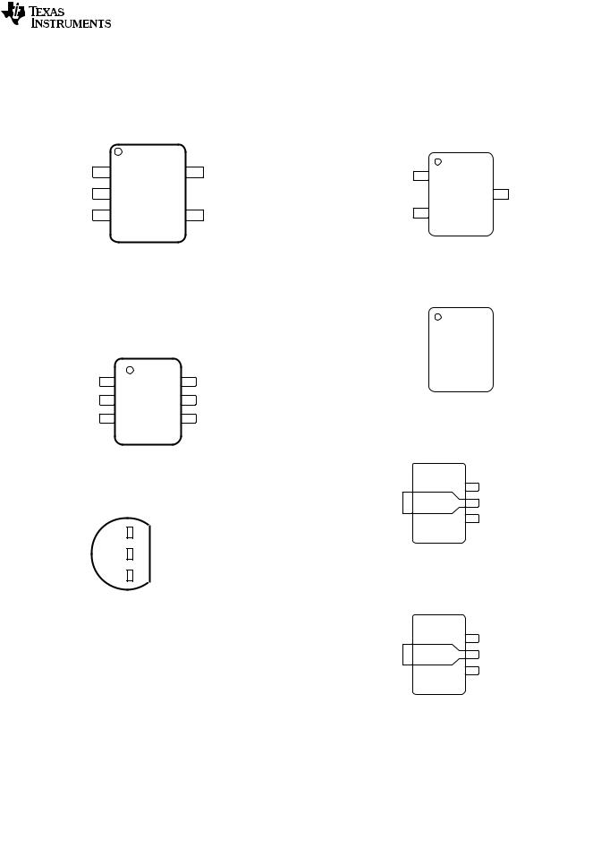
5 Pin Configuration and Functions
TLVH431 DBV Package
|
5-Pin SOT-23 |
|
|
TLVH431 DBZ Package |
|
|
|
|
|
|
3-Pin SOT-23 |
|
|
|
Top View |
|
|
|
|
|
|
|
|
|
Top View |
|
|
|
|
|
|
|
|
|
NC |
1 |
5 |
ANODE |
REF |
1 |
|
|
|
|
|
|
||
* |
2 |
|
|
|
3 |
ANODE |
CATHODE |
3 |
4 |
REF |
CATHODE |
2 |
|
|
|
|
||||
NOT TO SCALE
NOT TO SCALE
NC – No internal connection
* Pin 2 is attached to Substrate and must be connected to ANODE or left open.
TLVH431 DCK Package
6-Pin SC70
Top View
TLVH432 DBZ Package
3-Pin SOT-23
Top View
CATHODE  1
1
3  ANODE
ANODE
REF  2
2
CATHODE |
1 |
6 |
ANODE |
|
|
|
NOT TO SCALE |
NC |
2 |
5 |
NC |
REF |
3 |
4 |
NC |
|
TLVH431 PK Package |
|
|
3-Pin SOT-89 |
|
NOT TO SCALE |
Top View |
|
TLVH431 LP Package |
3 |
CATHODE |
3-Pin TO-92 |
|
|
Top View |
2 |
ANODE |
|
|
1 |
REF |
1 |
CATHODE |
|
|
|
|
NOT TO SCALE |
|
2 |
ANODE |
|
|
3 |
REF |
TLVH432 PK Package |
|
|
|
||
NOT TO SCALE |
|
3-Pin SOT-89 |
|
|
Top View |
|
|
|
|
|
|
|
|
3 |
REF |
|
|
2 |
ANODE |
|
|
1 |
CATHODE |
|
|
NOT TO SCALE |
|
Pin Functions
|
|
|
|
|
PIN |
|
|
|
|
|
|
|
||
NAME |
|
|
|
TLVH431 |
|
TLVH432 |
|
TYPE |
DESCRIPTION |
|
||||
DBZ |
DBV |
|
LP |
|
DCK |
|
PK |
DBZ |
|
PK |
|
|
|
|
|
|
|
|
|
|
|
|
|||||||
CATHODE |
2 |
3 |
|
1 |
|
1 |
|
3 |
1 |
|
1 |
I/O |
Shunt Current/Voltage input |
|
REF |
1 |
4 |
|
3 |
|
3 |
|
1 |
2 |
|
3 |
I |
Threshold relative to common anode |
|
|
|
|
|
|
|
|
|
|
|
|
|
|
|
|
ANODE |
3 |
5 |
|
2 |
|
6 |
|
2 |
3 |
|
2 |
O |
Common pin, normally connected to ground |
|
|
|
|
|
|
|
|
|
|
|
|
|
|
|
|
NC |
— |
1 |
|
— |
|
2, 4, 5 |
|
— |
— |
|
— |
I |
No Internal Connection |
|
* |
— |
2 |
|
— |
|
— |
|
— |
— |
|
— |
I |
Substrate Connection |
|
|
|
|
|
|
|
|
|
|
|
|
|
|
|
|
Copyright © 2004–2020, Texas Instruments Incorporated |
|
|
|
|
|
Submit Documentation Feedback |
3 |
|||||||
Product Folder Links: TLVH431 TLVH431A TLVH431B TLVH432 TLVH432A TLVH432B

TLVH431, TLVH431A, TLVH431B
TLVH432, TLVH432A, TLVH432B
SLVS555L –NOVEMBER 2004–REVISED APRIL 2020 |
www.ti.com |
6 Specifications
6.1 Absolute Maximum Ratings
over operating free-air temperature range (unless otherwise noted)(1)
|
|
MIN |
MAX |
UNIT |
V |
Cathode voltage(2) |
|
20 |
V |
KA |
|
|
|
|
IK |
Cathode current |
–25 |
80 |
mA |
Iref |
Reference current |
–0.05 |
3 |
mA |
TJ |
Operating virtual junction temperature |
|
150 |
°C |
Tstg |
Storage temperature |
–65 |
150 |
°C |
(1)Stresses beyond those listed under Absolute Maximum Ratings may cause permanent damage to the device. These are stress ratings only, which do not imply functional operation of the device at these or any other conditions beyond those indicated under Recommended Operating Conditions. Exposure to absolute-maximum-rated conditions for extended periods may affect device reliability.
(2)Voltage values are with respect to the anode terminal, unless otherwise noted.
6.2 ESD Ratings
|
|
|
VALUE |
UNIT |
|
V(ESD) |
Electrostatic |
Human body model (HBM), per ANSI/ESDA/JEDEC JS-001(1) |
±2000 |
V |
|
discharge |
Charged device model (CDM), per JEDEC specification JESD22-C101(2) |
±1000 |
|||
|
|
(1)JEDEC document JEP155 states that 500-V HBM allows safe manufacturing with a standard ESD control process.
(2)JEDEC document JEP157 states that 250-V CDM allows safe manufacturing with a standard ESD control process.
6.3 |
Recommended Operating Conditions |
|
|
|
|
|
See(1) |
|
|
|
|
|
|
|
|
|
|
MIN |
MAX |
UNIT |
VKA |
Cathode voltage |
|
VREF |
18 |
V |
|
IK |
Cathode current (continuous) |
|
0.1 |
70 |
mA |
|
|
|
|
TLVH43x_C |
0 |
70 |
|
TA |
Operating free-air temperature |
|
TLVH43x_I |
–40 |
85 |
°C |
|
|
|
TLVH43x_Q |
–40 |
125 |
|
(1)Maximum power dissipation is a function of TJ(max), θJA, and TA. The maximum allowable power dissipation at any allowable ambient temperature is PD = (TJ(max) – TA) / θJA. Operating at the absolute maximum TJ of 150°C can affect reliability.
6.4 Thermal Information
|
|
|
|
TLVH43xx |
|
|
|
|
THERMAL METRIC(1) |
DCK |
PK |
DBV |
DBZ |
LP |
UNIT |
|
|
(SC70) |
(SOT-89) |
(SOT-23) |
(SOT-23) |
(TO-92) |
|
|
|
6 PINS |
3 PINS |
5 PINS |
3 PINS |
3 PINS |
|
RθJA |
Junction-to-ambient thermal resistance |
259 |
52 |
206 |
206 |
140 |
°C/W |
RθJC(top) |
Junction-to-case (top) thermal resistance |
87 |
9 |
131 |
76 |
55 |
°C/W |
(1)For more information about traditional and new thermal metrics, see the Semiconductor and IC Package Thermal Metrics application report.
4 |
Submit Documentation Feedback |
Copyright © 2004–2020, Texas Instruments Incorporated |
Product Folder Links: TLVH431 TLVH431A TLVH431B TLVH432 TLVH432A TLVH432B

TLVH431, TLVH431A, TLVH431B
TLVH432, TLVH432A, TLVH432B
www.ti.com |
SLVS555L –NOVEMBER 2004–REVISED APRIL 2020 |
6.5 TLVH43x Electrical Characteristics
at 25°C free-air temperature (unless otherwise noted)
|
|
|
|
|
|
|
|
|
|
|
|
|
TLVH431 |
|
|
|
|
|
|
PARAMETER |
|
|
|
|
|
TEST CONDITIONS |
|
|
|
TLVH432 |
|
UNIT |
|
|
|
|
|
|
|
|
|
|
|
|
MIN |
|
TYP |
MAX |
|
|
|
|
|
|
|
|
|
|
|
TA = 25°C |
|
1.222 |
1.24 |
|
1.258 |
|
|
VREF |
Reference voltage |
VKA = VREF, |
|
|
TA = full range, |
TLVH431C |
1.21 |
|
|
|
1.27 |
V |
||||
IK = 10 mA |
|
|
|
TLVH431I |
1.202 |
|
|
|
1.278 |
|||||||
|
|
|
|
|
|
|
|
|
See Figure 18(1) |
|
|
|
|
|||
|
|
|
|
|
|
|
|
|
TLVH431Q |
1.194 |
|
|
|
1.286 |
|
|
|
|
|
|
|
|
|
|
|
|
|
|
|
|
|||
|
|
|
VREF deviation over full |
|
|
|
|
|
|
TLVH431C |
|
4 |
|
12 |
|
|
V |
V = V |
|
, I |
|
= 10 mA, See Figure 18(1) |
TLVH431I |
|
6 |
|
20 |
mV |
|||||
|
REF(dev) |
temperature range(2) |
KA |
REF |
|
K |
|
|
|
|
|
|
|
|
|
|
|
|
|
|
|
|
|
|
|
TLVH431Q |
|
11 |
|
31 |
|
||
|
|
|
|
|
|
|
|
|
|
|
|
|
||||
DVREF |
Ratio of VREF change to |
IK = 10 mA, VK = VREF to 18 V, See Figure 19 |
|
|
|
–1.5 |
–2.7 |
mV/V |
||||||||
|
DVKA |
|
cathode voltage change |
|
|
|
||||||||||
|
|
|
|
|
|
|
|
|
|
|
|
|||||
Iref |
Reference terminal current |
IK = 10 mA, R1 = 10 kΩ, R2 = open, See Figure 19 |
|
0.1 |
|
0.5 |
μA |
|||||||||
|
|
|
Iref deviation over full |
IK = 10 mA, R1 = 10 kΩ, R2 = open, |
TLVH431C |
|
0.05 |
|
0.3 |
|
||||||
Iref(dev) |
TLVH431I |
|
0.1 |
|
0.4 |
μA |
||||||||||
temperature range(2) |
See Figure 19(1) |
|
|
|||||||||||||
|
|
|
TLVH431Q |
|
0.15 |
|
0.5 |
|
||||||||
|
|
|
|
|
|
|
|
|
|
|
|
|
||||
IK(min) |
Minimum cathode current |
VKA = VREF, See Figure 18 |
|
|
60 |
|
100 |
μA |
||||||||
for regulation |
|
|
|
|||||||||||||
IK(off) |
Off-state cathode current |
VREF = 0, VKA = 18 V, See Figure 20 |
|
|
0.02 |
|
0.1 |
μA |
||||||||
|z | |
Dynamic impedance(3) |
VKA = VREF, f ≤ 1 kHz, IK = 0.1 mA to 70 mA, |
|
|
0.25 |
|
0.4 |
Ω |
||||||||
|
KA |
|
See Figure 18 |
|
|
|
|
|
|
|
|
|
||||
(1) Full temperature ranges are –40°C to +125°C for TLVH431Q, –40°C to +85°C for TLVH431I, and 0°C to 70°C for TLVH431C.
(2) The deviation parameters VREF(dev) and Iref(dev) are defined as the differences between the maximum and minimum values obtained over
the rated temperature range. The average full-range temperature coefficient of the reference input voltage, αVREF, is defined as: |
||||||||||||
|
|
|
|
|
|
|
æ |
VREF( dev ) |
ö |
´ 10 |
6 |
|
|
|
|
|
|
|
|
ç |
|
÷ |
|
|
|
|
|
|
|
|
|
|
|
|
|
|||
|
aVREF |
|
æ ppm ö |
= |
è |
VREF (TA = 25°C ) ø |
|
|
|
|||
|
|
|
|
|
||||||||
|
|
ç |
|
÷ |
|
|
|
|
|
|
||
|
|
|
|
|
|
|
|
|
||||
|
|
|
è |
°C ø |
|
|
DTA |
|
|
|
|
|
where |
|
TA is the rated operating free-air temperature range of the device. |
||||||||||
αVREF can be positive or negative, depending on whether minimum VREF or maximum VREF, respectively, occurs at the lower temperature.
(3)The dynamic impedance is defined as:
ZKA = DVKA
DIK
When the device is operating with two external resistors (see Figure 19), the total dynamic impedance of the circuit is defined as:
|
|
DV |
|
|
æ |
|
R1 |
ö |
ZKA |
¢ = |
|
» |
ZKA |
´ ç 1 |
+ |
|
÷ |
|
|
|||||||
|
|
DI |
|
|
è |
|
R2 |
ø |
Copyright © 2004–2020, Texas Instruments Incorporated |
Submit Documentation Feedback |
5 |
Product Folder Links: TLVH431 TLVH431A TLVH431B TLVH432 TLVH432A TLVH432B |
|
|

TLVH431, TLVH431A, TLVH431B
TLVH432, TLVH432A, TLVH432B
SLVS555L –NOVEMBER 2004–REVISED APRIL 2020 |
www.ti.com |
6.6 TLVH43xA Electrical Characteristics
at 25°C free-air temperature (unless otherwise noted)
|
|
|
|
|
|
|
|
|
|
|
|
TLVH431A |
|
|
|
|
|
|
PARAMETER |
|
|
|
|
|
TEST CONDITIONS |
|
|
TLVH432A |
|
UNIT |
|
|
|
|
|
|
|
|
|
|
|
|
MIN |
TYP |
MAX |
|
|
|
|
|
|
|
|
|
|
|
TA = 25°C |
|
1.228 |
1.24 |
|
1.252 |
|
VREF |
Reference voltage |
VKA = VREF, |
|
|
TA = full range, |
TLVH431AC |
1.221 |
|
|
1.259 |
V |
||||
IK = 10 mA |
|
|
|
TLVH431AI |
1.215 |
|
|
1.265 |
|||||||
|
|
|
|
|
|
|
|
|
See Figure 18(1) |
|
|
|
|||
|
|
|
|
|
|
|
|
|
TLVH431AQ |
1.209 |
|
|
1.271 |
|
|
|
|
|
|
|
|
|
|
|
|
|
|
|
|||
|
|
|
VREF deviation over full |
|
|
|
|
|
|
TLVH431AC |
|
4 |
|
12 |
|
V |
V = V |
|
, I |
|
= 10 mA, See Figure 18(1) |
TLVH431AI |
|
6 |
|
20 |
mV |
||||
|
REF(dev) |
temperature range(2) |
KA |
REF |
|
K |
|
|
|
|
|
|
|
|
|
|
|
|
|
|
|
|
|
|
TLVH431AQ |
|
11 |
|
31 |
|
|
|
|
|
|
|
|
|
|
|
|
|
|
|
|||
DVREF |
Ratio of VREF change to |
VK = VREF to 18 V, IK = 10 mA, See Figure 19 |
|
|
–1.5 |
–2.7 |
mV/V |
||||||||
|
DVKA |
|
cathode voltage change |
|
|
||||||||||
|
|
|
|
|
|
|
|
|
|
|
|
||||
Iref |
Reference terminal current |
IK = 10 mA, R1 = 10 kΩ, R2 = open, See Figure 19 |
|
0.1 |
|
0.5 |
μA |
||||||||
|
|
|
Iref deviation over full |
IK = 10 mA, R1 = 10 kΩ, R2 = open, |
TLVH431AC |
|
0.05 |
|
0.3 |
|
|||||
Iref(dev) |
TLVH431AI |
|
0.1 |
|
0.4 |
μA |
|||||||||
temperature range(2) |
See Figure 19(1) |
|
|
||||||||||||
|
|
|
TLVH431AQ |
|
0.15 |
|
0.5 |
|
|||||||
|
|
|
|
|
|
|
|
|
|
|
|
|
|||
IK(min) |
Minimum cathode current |
VKA = VREF, See Figure 18 |
|
|
60 |
|
100 |
μA |
|||||||
for regulation |
|
|
|
||||||||||||
IK(off) |
Off-state cathode current |
VREF = 0, VKA = 18 V, See Figure 20 |
|
|
0.02 |
|
0.1 |
μA |
|||||||
|z | |
Dynamic impedance(3) |
VKA = VREF, f ≤ 1 kHz, IK = 0.1 mA to 70 mA, |
|
|
0.25 |
|
0.4 |
Ω |
|||||||
|
KA |
|
See Figure 18 |
|
|
|
|
|
|
|
|
||||
(1) Full temperature ranges are –40°C to +125°C for TLVH431Q, –40°C to +85°C for TLVH431I, and 0°C to 70°C for TLVH431C.
(2) The deviation parameters VREF(dev) and Iref(dev) are defined as the differences between the maximum and minimum values obtained over
the rated temperature range. The average full-range temperature coefficient of the reference input voltage, αVREF, is defined as: |
||||||||||||
|
|
|
|
|
|
|
æ |
VREF( dev ) |
ö |
´ 10 |
6 |
|
|
|
|
|
|
|
|
ç |
|
÷ |
|
|
|
|
|
|
|
|
|
|
|
|
|
|||
|
aVREF |
|
æ ppm ö |
= |
è |
VREF (TA = 25°C ) ø |
|
|
|
|||
|
|
|
|
|
||||||||
|
|
ç |
|
÷ |
|
|
|
|
|
|
||
|
|
|
|
|
|
|
|
|
||||
|
|
|
è |
°C ø |
|
|
DTA |
|
|
|
|
|
where |
|
TA is the rated operating free-air temperature range of the device. |
||||||||||
αVREF can be positive or negative, depending on whether minimum VREF or maximum VREF, respectively, occurs at the lower temperature.
(3)The dynamic impedance is defined as:
ZKA = DVKA
DIK
When the device is operating with two external resistors (see Figure 19), the total dynamic impedance of the circuit is defined as:
|
|
DV |
|
|
æ |
|
R1 |
ö |
ZKA |
¢ = |
|
» |
ZKA |
´ ç 1 |
+ |
|
÷ |
|
|
|||||||
|
|
DI |
|
|
è |
|
R2 |
ø |
6 |
Submit Documentation Feedback |
Copyright © 2004–2020, Texas Instruments Incorporated |
|
Product Folder Links: TLVH431 TLVH431A TLVH431B TLVH432 TLVH432A TLVH432B |
|

TLVH431, TLVH431A, TLVH431B
TLVH432, TLVH432A, TLVH432B
www.ti.com |
SLVS555L –NOVEMBER 2004–REVISED APRIL 2020 |
6.7 TLVH43xB Electrical Characteristics
at 25°C free-air temperature (unless otherwise noted)
|
|
|
|
|
|
|
|
|
|
|
|
|
|
TLVH431B |
|
|
|
|
|
|
PARAMETER |
|
|
|
|
|
|
|
TEST CONDITIONS |
|
|
TLVH432B |
|
UNIT |
|
|
|
|
|
|
|
|
|
|
|
|
|
|
MIN |
TYP |
MAX |
|
|
|
|
|
|
|
|
|
|
|
|
|
TA = 25°C |
|
1.234 |
1.24 |
|
1.246 |
|
VREF |
Reference voltage |
VKA = VREF, |
|
|
TA = full range, |
TLVH431BC |
1.227 |
|
|
1.253 |
V |
||||||
IK = 10 mA |
|
|
|
TLVH431BI |
1.224 |
|
|
1.259 |
|||||||||
|
|
|
|
|
|
|
|
|
|
|
See Figure 18(1) |
|
|
|
|||
|
|
|
|
|
|
|
|
|
|
|
TLVH431BQ |
1.221 |
|
|
1.265 |
|
|
|
|
|
|
|
|
|
|
|
|
|
|
|
|
|
|||
|
|
|
VREF deviation over full |
|
|
|
|
|
|
|
|
TLVH431BC |
|
4 |
|
12 |
|
V |
V |
|
= V |
|
, I |
|
= 10 mA, See Figure 18(1) |
TLVH431BI |
|
6 |
|
20 |
mV |
||||
|
REF(dev) |
temperature range(2) |
|
KA |
|
REF |
|
K |
|
|
|
|
|
|
|
|
|
|
|
|
|
|
|
|
|
|
|
|
TLVH431BQ |
|
11 |
|
31 |
|
|
|
|
|
|
|
|
|
|
|
|
|
|
|
|
|
|||
DVREF |
Ratio of VREF change to |
IK = 10 mA, VK = VREF to 18 V, See Figure 19 |
|
|
–1.5 |
–2.7 |
mV/V |
||||||||||
|
DVKA |
|
cathode voltage change |
|
|
||||||||||||
|
|
|
|
|
|
|
|
|
|
|
|
||||||
Iref |
Reference terminal current |
IK = 10 mA, R1 = 10 kΩ, R2 = open, See Figure 19 |
|
0.1 |
|
0.5 |
μA |
||||||||||
|
|
|
Iref deviation over full |
IK = 10 mA, R1 = 10 kΩ, R2 = open, |
TLVH431BC |
|
0.05 |
|
0.3 |
|
|||||||
Iref(dev) |
TLVH431BI |
|
0.1 |
|
0.4 |
μA |
|||||||||||
temperature range(2) |
See Figure 19(1) |
|
|
||||||||||||||
|
|
|
TLVH431BQ |
|
0.15 |
|
0.5 |
|
|||||||||
|
|
|
|
|
|
|
|
|
|
|
|
|
|
|
|||
IK(min) |
Minimum cathode current |
VKA = VREF, See Figure 18 |
|
|
60 |
|
100 |
μA |
|||||||||
for regulation |
|
|
|
||||||||||||||
IK(off) |
Off-state cathode current |
VREF = 0, VKA = 18 V, See Figure 20 |
|
|
0.02 |
|
0.1 |
μA |
|||||||||
|z | |
Dynamic impedance(3) |
V |
KA |
= V |
REF |
, f ≤ 1 kHz, I = 0.1 mA to 70 mA, See Figure 18 |
|
0.25 |
|
0.4 |
Ω |
||||||
|
KA |
|
|
|
|
|
|
K |
|
|
|
|
|
|
|||
(1) Full temperature ranges are –40°C to +125°C for TLVH431Q, –40°C to +85°C for TLVH431I, and 0°C to 70°C for TLVH431C.
(2) The deviation parameters VREF(dev) and Iref(dev) are defined as the differences between the maximum and minimum values obtained over
the rated temperature range. The average full-range temperature coefficient of the reference input voltage, αVREF, is defined as: |
||||||||||||
|
|
|
|
|
|
|
æ |
VREF( dev ) |
ö |
´ 10 |
6 |
|
|
|
|
|
|
|
|
ç |
|
÷ |
|
|
|
|
|
|
|
|
|
|
|
|
|
|||
|
aVREF |
|
æ ppm ö |
= |
è |
VREF (TA = 25°C ) ø |
|
|
|
|||
|
|
|
|
|
||||||||
|
|
ç |
|
÷ |
|
|
|
|
|
|
||
|
|
|
|
|
|
|
|
|
||||
|
|
|
è |
°C ø |
|
|
DTA |
|
|
|
|
|
where |
|
TA is the rated operating free-air temperature range of the device. |
||||||||||
αVREF can be positive or negative, depending on whether minimum VREF or maximum VREF, respectively, occurs at the lower temperature.
(3)The dynamic impedance is defined as:
ZKA = DVKA
DIK
When the device is operating with two external resistors (see Figure 19), the total dynamic impedance of the circuit is defined as:
|
|
DV |
|
|
æ |
|
R1 |
ö |
ZKA |
¢ = |
|
» |
ZKA |
´ ç 1 |
+ |
|
÷ |
|
|
|||||||
|
|
DI |
|
|
è |
|
R2 |
ø |
Copyright © 2004–2020, Texas Instruments Incorporated |
Submit Documentation Feedback |
7 |
Product Folder Links: TLVH431 TLVH431A TLVH431B TLVH432 TLVH432A TLVH432B |
|
|
TLVH431, TLVH431A, TLVH431B
TLVH432, TLVH432A, TLVH432B
SLVS555L –NOVEMBER 2004–REVISED APRIL 2020 |
www.ti.com |
6.8 Typical Characteristics
Operation of the device at these or any other conditions beyond those indicated in the Recommended Operating Conditions table are not implied.
|
1.254 |
|
|
|
|
|
|
|
|
|
250 |
|
|
|
|
|
|
|
|
|
|
IK = 10 mA |
|
|
|
|
|
|
|
230 |
IK = 10 mA |
|
|
|
|
|
|
||
|
1.252 |
|
|
|
|
|
|
|
|
|
|
|
|
|
|
|
|||
|
|
|
|
|
|
|
|
|
|
|
R1 = 10 kΩ |
|
|
|
|
|
|
||
|
|
|
|
|
|
|
|
|
|
<![if ! IE]> <![endif]>nA |
|
|
|
|
|
|
|
||
| <![if ! IE]> <![endif]>V |
|
|
|
|
|
|
|
|
|
210 |
R2 = Open |
|
|
|
|
|
|
||
1.250 |
|
|
|
|
|
|
|
|
<![if ! IE]> <![endif]>− |
|
|
|
|
|
|
|
|
|
|
| <![if ! IE]> <![endif]>Reference Voltage − |
|
|
|
|
|
|
|
|
<![if ! IE]> <![endif]>Input Current |
|
|
|
|
|
|
|
|
|
|
|
|
|
|
|
|
|
|
|
190 |
|
|
|
|
|
|
|
|
||
1.248 |
|
|
|
|
|
|
|
|
170 |
|
|
|
|
|
|
|
|
||
|
|
|
|
|
|
|
|
|
|
|
|
|
|
|
|
|
|||
1.246 |
|
|
|
|
|
|
|
|
150 |
|
|
|
|
|
|
|
|
||
1.244 |
|
|
|
|
|
|
|
|
130 |
|
|
|
|
|
|
|
|
||
|
|
|
|
|
|
|
|
|
|
|
|
|
|
|
|
|
|||
| <![if ! IE]> <![endif]>− |
|
|
|
|
|
|
|
|
|
<![if ! IE]> <![endif]>Reference |
110 |
|
|
|
|
|
|
|
|
| <![if ! IE]> <![endif]>ref |
|
|
|
|
|
|
|
|
|
|
|
|
|
|
|
|
|
||
1.242 |
|
|
|
|
|
|
|
|
|
|
|
|
|
|
|
|
|
||
| <![if ! IE]> <![endif]>V |
|
|
|
|
|
|
|
|
|
<![if ! IE]> <![endif]>− |
90 |
|
|
|
|
|
|
|
|
|
|
|
|
|
|
|
|
|
|
<![if ! IE]> <![endif]>ref |
|
|
|
|
|
|
|
|
|
|
|
|
|
|
|
|
|
|
|
|
|
|
|
|
|
|
|
|
|
|
1.240 |
|
|
|
|
|
|
|
|
<![if ! IE]> <![endif]>I |
|
|
|
|
|
|
|
|
|
|
|
|
|
|
|
|
|
|
|
70 |
|
|
|
|
|
|
|
|
|
|
|
|
|
|
|
|
|
|
|
|
|
|
|
|
|
|
|
|
|
|
1.238 |
|
|
|
|
|
|
|
|
|
50 |
|
|
|
|
|
|
|
|
|
− 50 |
− 25 |
0 |
25 |
50 |
75 |
100 |
125 |
150 |
|
−50 |
−25 |
0 |
25 |
50 |
75 |
100 |
125 |
150 |
|
|
|
TJ − Junction Temperature − °C |
|
|
|
|
|
TJ − Junction Temperature − °C |
|
|
||||||||
Figure 1. Reference Voltage
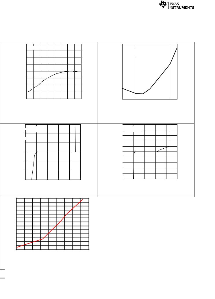
vs Junction Temperature
Figure 2. Reference Input Current
vs Junction Temperature
|
70 |
|
|
|
|
|
|
|
|
250 |
VKA = VREF |
|
|
|
|
|
V |
KA |
= V |
|
|
|
|
|
|
|
|
|
|
||
|
~ T |
REF |
|
|
|
|
|
TA = 25°C |
|
|
|
|
|||
|
|
= 25°C |
|
|
|
|
|
200 |
|
|
|
|
|||
|
A |
|
|
|
|
|
|
|
|
|
|
|
|
|
|
|
10 |
|
|
|
|
|
|
|
|
150 |
|
|
|
|
|
| <![if ! IE]> <![endif]>mA |
|
|
|
|
|
|
|
|
|
|
|
|
|
|
|
~ |
|
|
|
|
|
|
|
<![if ! IE]> <![endif]>µA |
100 |
|
|
|
|
|
|
|
|
|
|
|
|
|
|
|
|
|
|
|
|||
| <![if ! IE]> <![endif]>− |
5 |
|
|
|
|
|
|
|
<![if ! IE]> <![endif]>− |
|
|
|
|
|
|
|
|
|
|
|
|
|
|
|
|
|
|
|
|||
| <![if ! IE]> <![endif]>Current |
|
|
|
|
|
|
|
<![if ! IE]> <![endif]>Current |
|
|
|
|
|
|
|
|
|
|
|
|
|
|
|
50 |
|
|
|
|
|
||
0 |
|
|
|
|
|
|
|
0 |
|
|
|
|
|
||
| <![if ! IE]> <![endif]>Cathode |
|
|
|
|
|
|
|
<![if ! IE]> <![endif]>Cathode |
|
|
|
|
|
||
|
|
|
|
|
|
|
|
− 50 |
|
|
|
|
|
||
− 5 |
|
|
|
|
|
|
|
|
|
|
|
|
|
||
| <![if ! IE]> <![endif]>− |
|
|
|
|
|
|
|
|
<![if ! IE]> <![endif]>− |
− 100 |
|
|
|
|
|
| <![if ! IE]> <![endif]>K |
|
|
|
|
|
|
|
|
|
|
|
|
|
||
|
|
|
|
|
|
|
|
|
|
|
|
|
|
||
| <![if ! IE]> <![endif]>I |
|
|
|
|
|
|
|
|
<![if ! IE]> <![endif]>K |
|
|
|
|
|
|
|
|
|
|
|
|
|
|
|
<![if ! IE]> <![endif]>I |
|
|
|
|
|
|
|
− 10 |
|
|
|
|
|
|
|
|
− 150 |
|
|
|
|
|
|
|
|
|
|
|
|
|
|
|
|
|
|
|
|
|
|
|
|
|
|
|
|
|
|
|
− 200 |
|
|
|
|
|
|
− 15 |
|
|
|
|
|
|
|
|
− 250 |
|
|
|
|
|
|
− 1 |
|
|
− 0.5 |
0 |
0.5 |
1 |
1.5 |
|
− 1 |
− 0.5 |
0 |
0.5 |
1 |
1.5 |
|
|
|
|
|
VKA − Cathode Voltage − V |
|
|
|
|
VKA − Cathode Voltage − V |
|
|
|||
Figure 3. Cathode Current |
Figure 4. Cathode Current |
vs Cathode Voltage |
vs Cathode Voltage |
|
120 |
|
|
|
|
|
|
|
|
|
|
115 |
|
|
|
|
|
|
|
|
<![if ! IE]> <![endif]>nA |
|
110 |
|
|
|
|
|
|
|
|
|
|
|
|
|
|
|
|
|
|
<![if ! IE]> <![endif]>− |
|
|
|
|
|
|
|
|
|
|
|
|
|
105 |
|
|
|
|
|
|
|
|
<![if ! IE]> <![endif]>Current |
|
|
|
|
|
|
|
|
|
|
|
|
100 |
|
|
|
|
|
|
|
|
|
| <![if ! IE]> <![endif]>Ik(min) |
95 |
|
|
|
|
|
|
|
|
<![if ! IE]> <![endif]>State-Off− Cathode |
70 |
|
|
|
|
|
|
|
|
||
|
90 |
|
|
|
|
|
|
|
|
|
|
85 |
|
|
|
|
|
|
|
|
|
|
80 |
|
|
|
|
|
|
|
|
|
|
75 |
|
|
|
|
|
|
|
|
|
|
65 |
|
|
|
|
|
|
|
|
<![if ! IE]> <![endif]>K(off) |
|
|
|
|
|
|
|
|
|
|
|
|
60 |
|
|
|
|
|
|
|
|
<![if ! IE]> <![endif]>I |
|
55 |
|
|
|
|
|
|
|
|
|
|
-40 |
-20 |
0 |
20 |
40 |
60 |
80 |
100 |
120 |
140 |
|
|
|
|
|
Temperature (qC) |
|
|
|
|
|
Figure 5. Minimum Cathode Current vs. Temperature
4000 |
|
|
|
|
|
|
|
|
3500 |
VKA = 5 V |
|
|
|
|
|
|
|
VREF |
= 0 |
|
|
|
|
|
|
|
|
|
|
|
|
|
|
||
3000 |
|
|
|
|
|
|
|
|
2500 |
|
|
|
|
|
|
|
|
2000 |
|
|
|
|
|
|
|
|
1500 |
|
|
|
|
|
|
|
|
1000 |
|
|
|
|
|
|
|
|
500 |
|
|
|
|
|
|
|
|
0 |
|
|
|
|
|
|
|
|
−50 |
−25 |
0 |
25 |
50 |
75 |
100 |
125 |
150 |
TJ − Junction Temperature − °C
Figure 6. Off-State Cathode Current
vs Junction Temperature
8 |
Submit Documentation Feedback |
Copyright © 2004–2020, Texas Instruments Incorporated |
Product Folder Links: TLVH431 TLVH431A TLVH431B TLVH432 TLVH432A TLVH432B
TLVH431, TLVH431A, TLVH431B
TLVH432, TLVH432A, TLVH432B
www.ti.com |
SLVS555L –NOVEMBER 2004–REVISED APRIL 2020 |
Typical Characteristics (continued)
Operation of the device at these or any other conditions beyond those indicated in the Recommended Operating Conditions table are not implied.
| <![if ! IE]> <![endif]>VoltageReference |
<![if ! IE]> <![endif]>mV/V− |
0.00 |
|
|
|
|
|
|
|
|
<![if ! IE]> <![endif]>V |
0.025 |
|
|
|
|
|
|
−0.1 |
IK = 10 mA |
|
|
|
|
|
|
|
IK = 1 mA |
|
|
|
|
|||||
|
|
|
|
|
|
|
|
|
|
|
|
|
|
|||||
|
|
|
|
|
|
|
|
|
|
|
|
|
|
|
|
|||
|
|
|
VKA = VREF to 18 V |
|
|
|
|
|
|
0 |
|
|
|
|
|
|
||
|
|
−0.2 |
|
|
|
|
|
|
|
|
<![if ! IE]> <![endif]>% |
|
|
|
|
|
|
|
|
|
|
|
|
|
|
|
|
|
|
|
|
|
|
|
|
||
|
|
|
|
|
|
|
|
|
|
|
<![if ! IE]> <![endif]>− |
|
|
|
|
|
|
|
|
|
−0.3 |
|
|
|
|
|
|
|
|
<![if ! IE]> <![endif]>ref |
|
|
|
|
|
|
|
|
|
|
|
|
|
|
|
|
|
|
<![if ! IE]> <![endif]>ref |
|
|
|
% Change (avg) |
|
|
|
| <![if ! IE]> <![endif]>V |
<![if ! IE]> <![endif]>VoltageCathodeDeltato |
|
|
|
|
|
|
|
|
|
<![if ! IE]> <![endif]>VinChangePercentage |
− 0.025 |
|
|
|
|
||
|
|
|
|
|
|
|
|
|
|
|
|
|
|
|
|
|
|
|
| <![if ! IE]> <![endif]>Delta |
|
−0.4 |
|
|
|
|
|
|
|
|
|
|
|
% Change (3δ) |
|
|
|
|
|
|
|
|
|
|
|
|
|
|
|
|
|
|
|
|
|||
|
−0.5 |
|
|
|
|
|
|
|
|
|
− 0.05 |
|
|
|
|
|
|
|
| <![if ! IE]> <![endif]>of |
|
|
|
|
|
|
|
|
|
|
|
|
|
|
|
|
|
|
| <![if ! IE]> <![endif]>Ratio |
|
−0.6 |
|
|
|
|
|
|
|
|
|
|
|
|
|
|
|
|
|
−0.7 |
|
|
|
|
|
|
|
|
|
− 0.075 |
|
|
|
|
|
|
|
| <![if ! IE]> <![endif]>− |
|
|
|
|
|
|
|
|
|
|
|
|
|
|
|
|
|
|
| <![if ! IE]> <![endif]>KA |
|
−0.8 |
|
|
|
|
|
|
|
|
|
|
|
|
|
|
|
|
|
|
|
|
|
|
|
|
|
|
|
|
|
|
|
|
|
|
|
| <![if ! IE]> <![endif]>ref/ |
|
|
|
|
|
|
|
|
|
|
|
− 0.1 |
|
|
|
|
|
|
|
−0.9 |
|
|
|
|
|
|
|
|
|
|
% Change (−3δ) |
|
|
|
|||
| <![if ! IE]> <![endif]>V |
|
|
|
|
|
|
|
|
|
|
|
|
|
|
|
|||
|
|
−1−.10 |
|
|
|
|
|
|
|
|
|
− 0.125 |
|
|
|
|
|
|
|
|
−50 |
−25 |
0 |
25 |
50 |
75 |
100 |
125 |
150 |
|
|
|
|
|
|
|
|
|
|
|
0 |
10 |
20 |
30 |
40 |
50 |
60 |
|||||||||
|
|
|
|
|
|
|
|
|
|
|
|
|||||||
|
|
|
|
TJ − Junction Temperature − °C |
|
|
|
|
Operating Life at 55°C − kh(1) |
|
|
|||||||
|
|
|
|
|
|
|
|
|
|
|
(1) Extrapolated from life-test data taken at 125°C; the activation energy |
|||||||
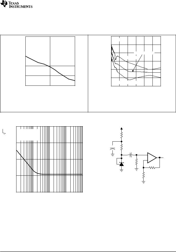
Figure 7. Ratio of Delta Reference Voltage to Delta Cathode |
assumed is 0.7 eV. |
Figure 8. Percentage Change in VREF |
|
Voltage |
vs |
vs Junction Temperature |
Operating Life at 55°C |
EQUIVALENT INPUT NOISE VOLTAGE vs
FREQUENCY
| <![if ! IE]> <![endif]>Hz) |
350 |
|
|
|
|
|
VKA = VREF |
|
|
|
|
| <![if ! IE]> <![endif]>(nV/ |
|
IK = 1 mA |
|
|
|
|
TA = 25°C |
|
|
|
|
| <![if ! IE]> <![endif]>− |
300 |
|
|
|
|
| <![if ! IE]> <![endif]>Voltage |
|
|
|
|
|
|
|
|
|
|
|
| <![if ! IE]> <![endif]>InputNoise |
250 |
|
|
|
|
|
|
|
|
|
|
| <![if ! IE]> <![endif]>−Equivalent |
200 |
|
|
|
|
|
|
|
|
|
|
| <![if ! IE]> <![endif]>n |
|
|
|
|
|
| <![if ! IE]> <![endif]>V |
|
|
|
|
|
|
150 |
|
|
|
|
|
10 |
100 |
1 k |
10 k |
100 k |
|
|
|
f – Frequency – (Hz) |
|
|
|
3 V |
|
|
|
1 kW |
|
|
+ |
750 W |
|
|
470 mF |
2200 mF |
TLE2027 |
|
|
|
||
|
|
|
|
|
+ |
+ |
|
|
|
|
|
|
|
_ |
TP |
|
|
|
|
TLVH431 |
820 W |
|
|
|
|
|
|
TLVH432 |
|
|
|
|
|
160 kW |
|
|
160 W |
|
|
TEST CIRCUIT FOR EQUIVALENT INPUT NOISE VOLTAGE
Figure 9. Equivalent Input Noise Voltage
Copyright © 2004–2020, Texas Instruments Incorporated |
Submit Documentation Feedback |
9 |
Product Folder Links: TLVH431 TLVH431A TLVH431B TLVH432 TLVH432A TLVH432B
TLVH431, TLVH431A, TLVH431B
TLVH432, TLVH432A, TLVH432B
SLVS555L –NOVEMBER 2004–REVISED APRIL 2020 |
www.ti.com |
Typical Characteristics (continued)
Operation of the device at these or any other conditions beyond those indicated in the Recommended Operating Conditions table are not implied.
EQUIVALENT INPUT NOISE VOLTAGE
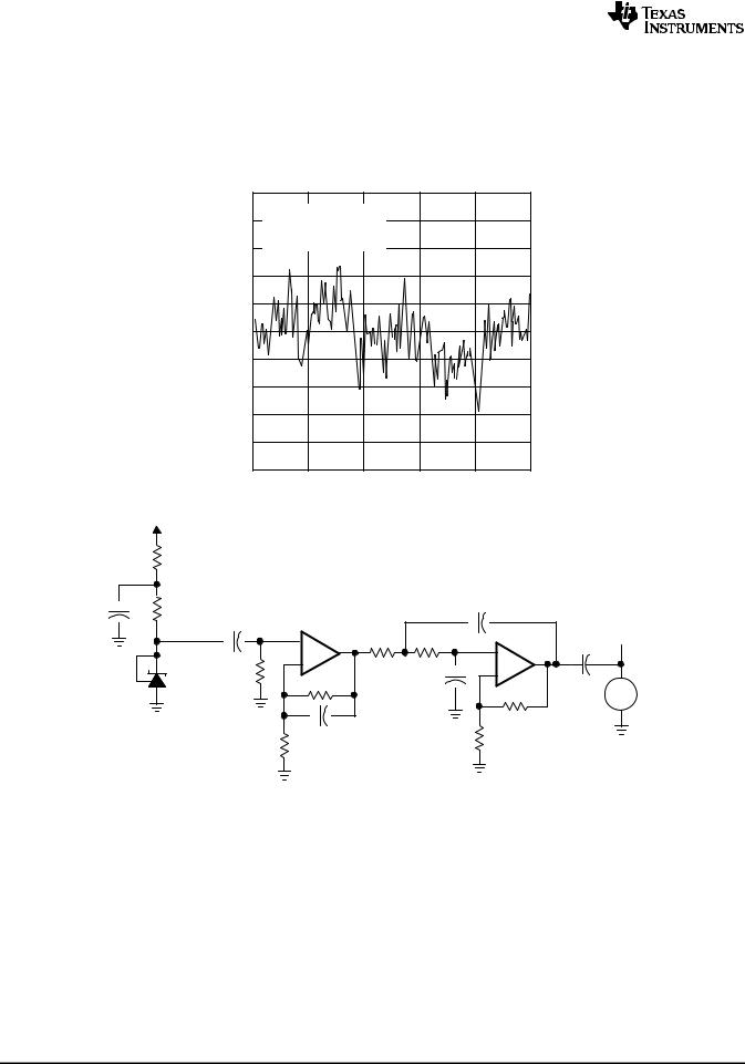
OVER A 10-S PERIOD
|
10 |
|
|
|
|
|
| <![if ! IE]> <![endif]>(mV) |
8 |
f = 0.1 Hz to 10 Hz |
|
|
|
|
IK = 1 mA |
|
|
|
|
||
|
|
|
|
|
||
| <![if ! IE]> <![endif]>− |
|
TA = 25°C |
|
|
|
|
| <![if ! IE]> <![endif]>Voltage |
6 |
|
|
|
|
|
|
|
|
|
|
||
4 |
|
|
|
|
|
|
|
|
|
|
|
|
|
| <![if ! IE]> <![endif]>Noise |
2 |
|
|
|
|
|
|
|
|
|
|
|
|
| <![if ! IE]> <![endif]>Input |
0 |
|
|
|
|
|
|
|
|
|
|
|
|
| <![if ! IE]> <![endif]>Equivalent |
− 2 |
|
|
|
|
|
− 4 |
|
|
|
|
|
|
− 6 |
|
|
|
|
|
|
| <![if ! IE]> <![endif]>− |
|
|
|
|
|
|
|
|
|
|
|
|
|
| <![if ! IE]> <![endif]>n |
|
|
|
|
|
|
| <![if ! IE]> <![endif]>V |
− 8 |
|
|
|
|
|
|
|
|
|
|
|
|
|
− 10 |
|
|
|
|
|
|
0 |
2 |
4 |
6 |
8 |
10 |
|
|
|
t − Time − (s) |
|
|
|
|
|
3 V |
|
|
|
|
|
|
|
|
1 kW |
|
|
|
|
|
|
|
+ |
750 W |
|
|
|
0.47 mF |
|
|
470 mF |
|
|
|
|
|
|
|
|
|
2200 mF |
|
|
|
|
|
|
|
|
|
TLE2027 |
|
|
|
|
|
|
|
|
+ |
|
|
TLE2027 |
TP |
|
|
|
|
+ |
10 kW |
10 kW |
|
|||
|
|
|
2.2 mF |
|
||||
|
|
|
+ |
|
||||
|
|
|
_ |
|
|
+ |
|
|
|
|
|
|
|
|
|
||
|
|
820 W |
|
|
|
_ |
|
|
|
|
160 kW |
|
1 mF |
|
|
|
|
TLVH431 |
|
|
|
|
|
1 MW |
||
|
|
|
|
|
|
CRO |
||
TLVH432 |
|
|
|
|
|
|
|
|
|
|
|
|
|
|
33 kW |
|
|
|
|
16 W |
0.1 mF |
|
33 kW |
|
|
|
|
|
|
|
|
|
|
|
|
TEST CIRCUIT FOR 0.1-Hz TO 10-Hz EQUIVALENT NOISE VOLTAGE
Figure 10. Equivalent Input Noise Voltage
10 |
Submit Documentation Feedback |
Copyright © 2004–2020, Texas Instruments Incorporated |
Product Folder Links: TLVH431 TLVH431A TLVH431B TLVH432 TLVH432A TLVH432B
TLVH431, TLVH431A, TLVH431B
TLVH432, TLVH432A, TLVH432B
www.ti.com |
SLVS555L –NOVEMBER 2004–REVISED APRIL 2020 |
Typical Characteristics (continued)
Operation of the device at these or any other conditions beyond those indicated in the Recommended Operating Conditions table are not implied.
SMALL-SIGNAL VOLTAGE GAIN
/PHASE MARGIN vs FREQUENCY
| <![if ! IE]> <![endif]>(dB) |
80 |
|
|
|
0° |
|
|
|
|
IK = 10 mA |
|
|
|
| <![if ! IE]> <![endif]>− |
70 |
|
|
TA = 25°C |
36° |
|
| <![if ! IE]> <![endif]>Gain/PhaseMargin |
|
|
<![if ! IE]> <![endif]>PhaseShift |
|||
60 |
|
|
|
72° |
||
50 |
|
|
|
108° |
||
40 |
|
|
|
144° |
||
|
|
|
|
180° |
||
| <![if ! IE]> <![endif]>Voltage |
30 |
|
|
|
|
|
20 |
|
|
|
|
|
|
|
|
|
|
|
|
|
| <![if ! IE]> <![endif]>Small-Signal |
10 |
|
|
|
|
|
0 |
|
|
|
|
|
|
− 10 |
|
|
|
|
|
|
| <![if ! IE]> <![endif]>− |
|
|
|
|
|
|
|
|
|
|
|
|
|
| <![if ! IE]> <![endif]>V |
− 20 |
|
|
|
|
|
| <![if ! IE]> <![endif]>A |
|
|
|
|
|
|
100 |
1 k |
10 k |
100 k |
1 M |
|
|
|
|
|||||
|
|
|
f − Frequency − (Hz) |
|
|
|
|
Output |
6.8 kW |
IK |
|
180 W |
10 mF |
|
|
5 V |
4.3 kW |
|
|
GND |
TEST CIRCUIT FOR VOLTAGE GAIN
AND PHASE MARGIN
|
|
|
|
Figure 11. Voltage Gain and Phase Margin |
|
|
|||||
|
|
PULSE RESPONSE 1 |
|
|
|
|
|||||
|
3.5 |
|
|
|
|
|
R = 18 kΩ |
|
|
|
|
|
|
|
|
|
|
|
|
|
|
||
|
3 |
|
Input |
|
|
TA = 25°C |
|
|
|
||
|
|
|
|
|
|
|
|
|
18 kΩ |
||
|
|
|
|
|
|
|
|
|
|
||
| <![if ! IE]> <![endif]>−V |
2.5 |
|
|
|
|
|
|
|
|
|
Output |
|
|
|
|
|
|
|
|
|
|
||
| <![if ! IE]> <![endif]>Voltage |
2 |
|
|
|
|
|
|
|
Pulse |
|
Ik |
|
|
|
|
|
|
|
|
|
|
||
| <![if ! IE]> <![endif]>Output |
|
|
|
|
|
|
|
|
|
|
|
|
|
|
|
|
|
|
|
Generator |
50 |
Ω |
|
|
|
|
|
|
|
|
|
|
|||
|
1.5 |
|
|
|
|
|
|
|
|
||
|
|
Output |
|
|
|
|
f = 100 kHz |
|
|
||
|
|
|
|
|
|
|
|
|
|||
|
|
|
|
|
|
|
|
|
|
||
| <![if ! IE]> <![endif]>and |
1 |
|
|
|
|
|
|
|
|
|
|
| <![if ! IE]> <![endif]>Input |
0.5 |
|
|
|
|
|
|
|
|
|
GND |
|
|
|
|
|
|
|
|
|
|
|
|
|
0 |
|
|
|
|
|
|
|
TEST CIRCUIT FOR PULSE RESPONSE 1 |
||
|
|
|
|
|
|
|
|
|
|||
|
− 0.5 |
|
|
|
|
|
|
|
|
|
|
|
0 |
1 |
2 |
3 |
4 |
5 |
6 |
7 |
8 |
|
|
|
|
|
t − Time − µs |
|
|
|
|
|
|
||
Figure 12. Pulse Response 1
Copyright © 2004–2020, Texas Instruments Incorporated |
Submit Documentation Feedback |
11 |
Product Folder Links: TLVH431 TLVH431A TLVH431B TLVH432 TLVH432A TLVH432B
TLVH431, TLVH431A, TLVH431B
TLVH432, TLVH432A, TLVH432B
SLVS555L –NOVEMBER 2004–REVISED APRIL 2020 |
www.ti.com |
Typical Characteristics (continued)
Operation of the device at these or any other conditions beyond those indicated in the Recommended Operating Conditions table are not implied.
|
|
PULSE RESPONSE 2 |
|
|
|
|
|||||
|
3.5 |
|
|
|
|
|
R = 1.8 kΩ |
|
|
|
|
|
|
|
|
|
|
|
|
|
|
||
|
3 |
|
Input |
|
|
TA = 25°C |
|
|
|
||
|
|
|
|
|
|
|
|
|
1.8 kΩ |
||
|
|
|
|
|
|
|
|
|
|
||
| <![if ! IE]> <![endif]>−V |
2.5 |
|
|
|
|
|
|
|
|
|
Output |
|
|
|
|
|
|
|
|
|
|
||
| <![if ! IE]> <![endif]>Voltage |
2 |
|
|
|
|
|
|
|
Pulse |
|
IK |
|
|
|
|
|
|
|
|
|
|
||
| <![if ! IE]> <![endif]>Output |
|
|
|
|
|
|
|
|
|
|
|
|
|
|
|
|
|
|
|
Generator |
50 |
Ω |
|
|
|
|
|
|
|
|
|
|
|||
|
1.5 |
|
|
|
|
|
|
|
|
||
|
|
Output |
|
|
|
|
f = 100 kHz |
|
|
||
|
|
|
|
|
|
|
|
|
|||
| <![if ! IE]> <![endif]>and |
|
|
|
|
|
|
|
|
|
||
1 |
|
|
|
|
|
|
|
|
|
|
|
| <![if ! IE]> <![endif]>Input |
|
|
|
|
|
|
|
|
|
|
|
0.5 |
|
|
|
|
|
|
|
|
|
GND |
|
|
|
|
|
|
|
|
|
|
|
|
|
|
0 |
|
|
|
|
|
|
|
TEST CIRCUIT FOR PULSE RESPONSE 2 |
||
|
|
|
|
|
|
|
|
|
|||
|
− 0.5 |
|
|
|
|
|
|
|
|
|
|
|
0 |
1 |
2 |
3 |
4 |
5 |
6 |
7 |
8 |
|
|
|
|
|
t − Time − µs |
|
|
|
|
|
|
||
Figure 13. Pulse Response 2
|
|
30 kΩ |
|
|
|
IK |
|
50 |
Ω |
100 µF |
|
|
|
||
|
|
I2 |
CL |
|
|
I1 |
|
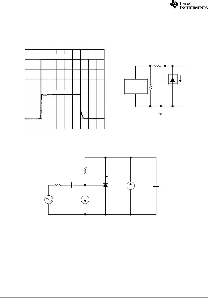
Figure 14. Phase Margin Test Circuit
12 |
Submit Documentation Feedback |
Copyright © 2004–2020, Texas Instruments Incorporated |
Product Folder Links: TLVH431 TLVH431A TLVH431B TLVH432 TLVH432A TLVH432B

TLVH431, TLVH431A, TLVH431B
TLVH432, TLVH432A, TLVH432B
www.ti.com |
SLVS555L –NOVEMBER 2004–REVISED APRIL 2020 |
Typical Characteristics (continued)
Operation of the device at these or any other conditions beyond those indicated in the Recommended Operating Conditions table are not implied.
IK
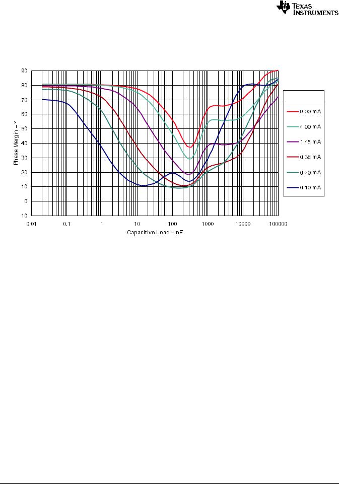
Figure 15. Phase Margin vs Capacitive Load
VKA = VREF (1.25 V), TA= 25°C
IK
Figure 16. Phase Margin vs Capacitive Load
VKA = 2.50 V, TA= 25°C
Copyright © 2004–2020, Texas Instruments Incorporated |
Submit Documentation Feedback |
13 |
Product Folder Links: TLVH431 TLVH431A TLVH431B TLVH432 TLVH432A TLVH432B
TLVH431, TLVH431A, TLVH431B
TLVH432, TLVH432A, TLVH432B
SLVS555L –NOVEMBER 2004–REVISED APRIL 2020 |
www.ti.com |
Typical Characteristics (continued)
Operation of the device at these or any other conditions beyond those indicated in the Recommended Operating Conditions table are not implied.
IK
Figure 17. Phase Margin vs Capacitive Load
VKA = 5.00 V, TA= 25°C
14 |
Submit Documentation Feedback |
Copyright © 2004–2020, Texas Instruments Incorporated |
Product Folder Links: TLVH431 TLVH431A TLVH431B TLVH432 TLVH432A TLVH432B
TLVH431, TLVH431A, TLVH431B
TLVH432, TLVH432A, TLVH432B
www.ti.com |
SLVS555L –NOVEMBER 2004–REVISED APRIL 2020 |
7 Parameter Measurement Information
Input |
VO |
|
IK |
|
VREF |
Figure 18. Test Circuit for VKA = VREF, VO = VKA = VREF
Input |
VO |
|
IK |
R1 |
Iref |
|
|
R2 |
VREF |
|
Figure 19. Test Circuit for VKA > VREF, VO = VKA = VREF × (1 + R1/R2) + Iref × R1
Input  VO
VO
IK(off)
Figure 20. Test Circuit for IK(off)
Copyright © 2004–2020, Texas Instruments Incorporated |
Submit Documentation Feedback |
15 |
Product Folder Links: TLVH431 TLVH431A TLVH431B TLVH432 TLVH432A TLVH432B
TLVH431, TLVH431A, TLVH431B
TLVH432, TLVH432A, TLVH432B
SLVS555L –NOVEMBER 2004–REVISED APRIL 2020 |
www.ti.com |
8 Detailed Description
8.1 Overview
TLVH431 is a low power counterpart to TL431, having lower reference voltage (1.24 V versus 2.5 V) for lower
voltage adjustability and lower minimum cathode current (Ik(min)= 100 µA versus 1 mA). Like TL431, TLVH431 is used in conjunction with its key components to behave as a single voltage reference, error amplifier, voltage
clamp or comparator with integrated reference.
TLVH431 is also a higher voltage counterpart to TLV431, with cathode voltage adjustability from 1.24 V to 18 V, making this part optimum for a wide range of end equipments in industrial, auto, telecom and computing. In order for this device to behave as a shunt regulator or error amplifier, >100 µA (Imin(max)) must be supplied in to the cathode pin. Under this condition, feedback can be applied from the Cathode and Ref pins to create a replica of the internal reference voltage.
Various reference voltage options can be purchased with initial tolerances (at 25°C) of 0.5%, 1%, and 1.5%. These reference options are denoted by B (0.5%), A (1.0%) and blank (1.5%) after the TLVH431.
The TLVH431xC devices are characterized for operation from 0°C to 70°C, the TLVH431xI devices are characterized for operation from –40°C to +85°C, and the TLVH431xQ devices are characterized for operation from –40°C to +125°C.
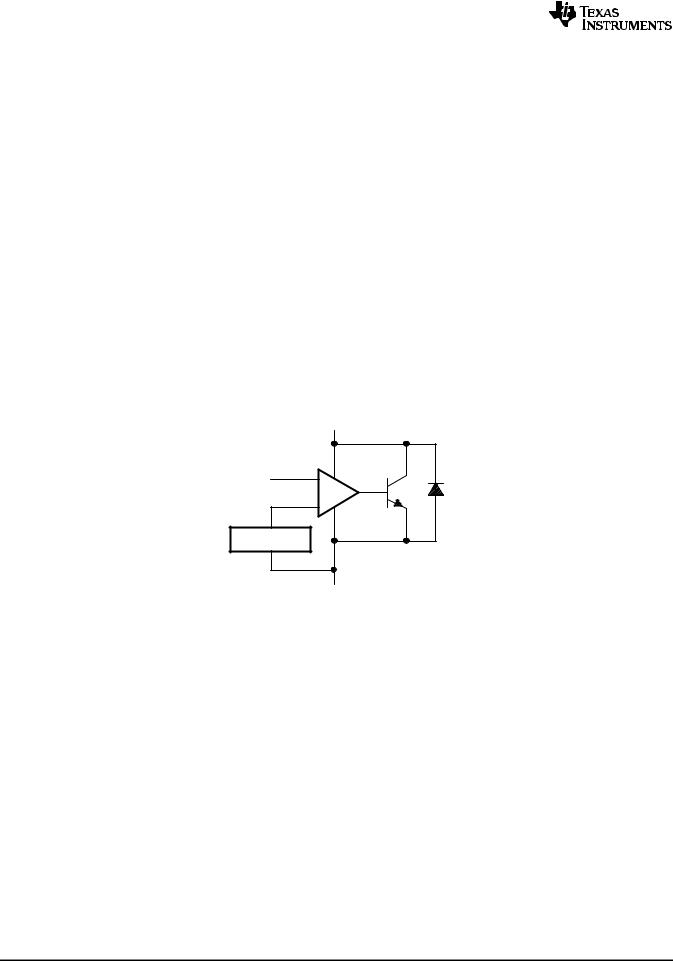
8.2 Functional Block Diagram
|
CATHODE |
REF |
+ |
|
− |
VREF = 1.24 V |
|
ANODE
Figure 21. Equivalent Schematic
16 |
Submit Documentation Feedback |
Copyright © 2004–2020, Texas Instruments Incorporated |
Product Folder Links: TLVH431 TLVH431A TLVH431B TLVH432 TLVH432A TLVH432B
TLVH431, TLVH431A, TLVH431B
TLVH432, TLVH432A, TLVH432B
www.ti.com |
SLVS555L –NOVEMBER 2004–REVISED APRIL 2020 |
Functional Block Diagram (continued)
CATHODE
REF |
ANODE
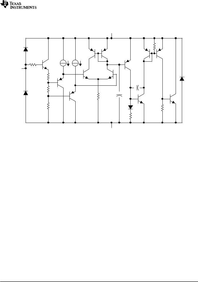
Figure 22. Detailed Schematic
8.3 Feature Description
TLVH431 consists of an internal reference and amplifier that outputs a sink current base on the difference between the reference pin and the virtual internal pin. The sink current is produced by an internal Darlington pair.
When operated with enough voltage headroom (≥ 1.24 V) and cathode current (Ika), TLVH431 forces the reference pin to 1.24 V. However, the reference pin can not be left floating, as it needs Iref ≥ 0.5 µA (see Specifications). This is because the reference pin is driven into an NPN, which needs base current in order operate properly.
When feedback is applied from the Cathode and Reference pins, TLVH431 behaves as a Zener diode, regulating to a constant voltage dependent on current being supplied into the cathode. This is due to the internal amplifier and reference entering the proper operating regions. The same amount of current needed in the above feedback situation must be applied to this device in open loop, servo or error amplifying implementations in order for it to be in the proper linear region giving TLVH431 enough gain.
Unlike many linear regulators, TLVH431 is internally compensated to be stable without an output capacitor between the cathode and anode. However, if it is desired to use an output capacitor Figure 15, Figure 16, and Figure 17 can be used as a guide to assist in choosing the correct capacitor to maintain stability.
Copyright © 2004–2020, Texas Instruments Incorporated |
Submit Documentation Feedback |
17 |
Product Folder Links: TLVH431 TLVH431A TLVH431B TLVH432 TLVH432A TLVH432B

TLVH431, TLVH431A, TLVH431B
TLVH432, TLVH432A, TLVH432B
SLVS555L –NOVEMBER 2004–REVISED APRIL 2020 |
www.ti.com |
8.4 Device Functional Modes
8.4.1 Open Loop (Comparator)
When the cathode/output voltage or current of TLVH431 is not being fed back to the reference/input pin in any form, this device is operating in open loop. With proper cathode current (Ika) applied to this device, TLVH431 has the characteristics shown in Figure 4. With such high gain in this configuration, the TLVH431 device is typically used as a comparator. With the reference integrated makes TLVH431 the preferred choice when users are trying to monitor a certain level of a single signal.
8.4.2 Closed Loop
When the cathode/output voltage or current of TLVH431 is being fed back to the reference/input pin in any form, this device is operating in closed loop. The majority of applications involving TLVH431 use it in this manner to regulate a fixed voltage or current. The feedback enables this device to behave as an error amplifier, computing a portion of the output voltage and adjusting it to maintain the desired regulation. This is done by relating the output voltage back to the reference pin in a manner to make it equal to the internal reference voltage, which can be accomplished through resistive or direct feedback.
18 |
Submit Documentation Feedback |
Copyright © 2004–2020, Texas Instruments Incorporated |
Product Folder Links: TLVH431 TLVH431A TLVH431B TLVH432 TLVH432A TLVH432B
Loading...