


TLV571 2.7 V TO 5.5 V, 1-CHANNEL, 8-BIT, PARALLEL ANALOG-TO-DIGITAL CONVERTER
SLAS239A ± SEPTEMBER 1999 ± REVISED FEBRUARY 2000
features
DFast Throughput Rate: 1.25 MSPS at 5 V,
625 KSPS at 3 V
DWide Analog Input: 0 V to AVDD
DDifferential Nonlinearity Error: < ± 0.5 LSB
DIntegral Nonlinearity Error: < ± 0.5 LSB
DSingle 2.7-V to 5.5-V Supply Operation
DLow Power: 12 mW at 3 V and 35 mW at 5 V
DAuto Power Down of 1 mA Max
DSoftware Power Down: 10 A Max
DInternal OSC
DHardware Configurable
DDSP and Microcontroller Compatible Parallel Interface
DBinary/Twos Complement Output
DHardware Controlled Extended Sampling
DHardware or Software Start of Conversion
description
applications
DMass Storage and HDD
DAutomotive
DDigital Servos
DProcess Control
DGeneral-Purpose DSP
DImage Sensor Processing
DW OR PW PACKAGE
(TOP VIEW)
|
|
|
|
|
|
|
|
|
|
|
|
|
|
|
CS |
|
|
1 |
24 |
|
|
NC |
|||
|
|
|
|
|
|
|||||||
|
|
WR |
|
|
|
2 |
23 |
|
|
AIN |
||
|
|
|
|
|
|
|
||||||
|
|
|
|
|
|
|
||||||
|
|
RD |
|
3 |
22 |
|
|
AVDD |
||||
|
|
|
|
|
|
|||||||
|
|
|
|
|
||||||||
|
CLK |
|
|
4 |
21 |
|
|
AGND |
||||
DGND |
|
5 |
20 |
|
|
REFM |
||||||
|
|
|
|
|||||||||
|
|
|
|
|||||||||
DVDD |
|
|
6 |
19 |
|
|
|
REFP |
||||
|
|
|
|
|
||||||||
|
|
|
|
|
|
|
|
|
|
|||
INT/EOC |
|
|
7 |
18 |
|
|
|
CSTART |
||||
DGND |
|
|
8 |
17 |
|
|
|
A1/D7 |
||||
|
|
|
|
|
||||||||
|
|
|
|
|
||||||||
DGND |
|
9 |
16 |
|
|
|
A0/D6 |
|||||
|
|
|
|
|
||||||||
|
|
|
|
|
||||||||
|
|
|
D0 |
|
|
10 |
15 |
|
|
|
D5 |
|
|
|
|
|
|
|
|
|
|||||
|
|
|
D1 |
|
11 |
14 |
|
|
|
D4 |
||
|
|
|
|
|
|
|
|
|||||
|
|
|
|
|
|
|
|
|||||
|
|
|
D2 |
|
|
12 |
13 |
|
|
|
D3 |
|
|
|
|
|
|
|
|
|
|||||
|
|
|
|
|
|
|
|
|
|
|
|
|
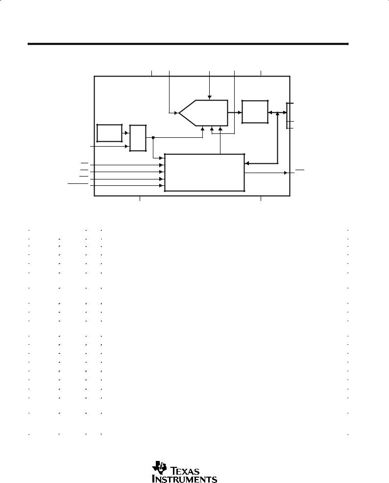
The TLV571 is an 8-bit data acquisition system that combines a high-speed 8-bit ADC and a
parallel interface. The device contains two on-chip control registers allowing control of software conversion start and power down via the bidirectional parallel port. The control registers can be set to a default mode using a dummy RD while WR is tied low allowing the registers to be hardware configurable.
The TLV571 operates from a single 2.7-V to 5.5-V power supply. It accepts an analog input range from 0 V to AVDD and digitizes the input at a maximum 1.25 MSPS throughput rate at 5 V. The power dissipations are only 12 mW with a 3-V supply or 35 mW with a 5-V supply. The device features an auto power-down mode that automatically powers down to 1 mA 50 ns after conversion is performed. In software power-down mode, the ADC is further powered down to only 10 A.
Very high throughput rate, simple parallel interface, and low power consumption make the TLV571 an ideal choice for high-speed digital signal processing.
AVAILABLE OPTIONS
|
|
PACKAGE |
|
TA |
|
|
|
24 TSSOP |
|
24 SOIC |
|
|
(PW) |
|
(DW) |
|
|
|
|
± 40°C to 85°C |
TLV571IPW |
|
TLV571IDW |
|
|
|
|
Please be aware that an important notice concerning availability, standard warranty, and use in critical applications of Texas Instruments semiconductor products and disclaimers thereto appears at the end of this data sheet.
PRODUCTION DATA information is current as of publication date. Products conform to specifications per the terms of Texas Instruments standard warranty. Production processing does not necessarily include testing of all parameters.
Copyright 2000, Texas Instruments Incorporated
POST OFFICE BOX 655303 •DALLAS, TEXAS 75265 |
1 |
TLV571
2.7 V TO 5.5 V, 1-CHANNEL, 8-BIT,
PARALLEL ANALOG-TO-DIGITAL CONVERTER
SLAS239A ± SEPTEMBER 1999 ± REVISED FEBRUARY 2000
functional block diagram
AV |
DD |
AIN |
REFP REFM |
DVDD |
|
|
|
|
Internal |
|
Clock |
MUX |
|
|
CLK |
|
CS
RD
WR
CSTART
|
Three |
D0 ± D5 |
|
8-BIT |
|
||
State |
|
||
SAR ADC |
|
||
Latch |
D6/A0 |
||
|
|||
|
|
||
|
|
D7/A1 |
|
Input Registers |
|
INT/EOC |
|
and Control Logic |
|
||
|
|
AGND DGND
|
|
|
|
|
|
|
|
Terminal Functions |
|
||||||||||||||
|
|
|
|
|
|
|
|
|
|
|
|
|
|
|
|
|
|
|
|
|
|
|
|
|
|
|
|
TERMINAL |
I/O |
|
|
|
|
|
|
|
|
DESCRIPTION |
|
||||||||
|
|
|
|
|
|
|
|
|
|
|
|
|
|
|
|
||||||||
|
NAME |
NO. |
|
|
|
|
|
|
|
|
|
|
|
|
|
|
|
|
|
||||
|
|
|
|
|
|
|
|
|
|
|
|
|
|
|
|
|
|
|
|
|
|
|
|
|
AGND |
21 |
|
Analog ground |
|
||||||||||||||||||
|
|
|
|
|
|
|
|
|
|
|
|
|
|
|
|
|
|
|
|
|
|
|
|
|
AIN |
23 |
I |
ADC analog input |
|
||||||||||||||||||
|
|
|
|
|
|
|
|
|
|
|
|
|
|
|
|
|
|
|
|
|
|
|
|
|
AVDD |
22 |
|
Analog supply voltage, 2.7 V to 5.5 V |
|
||||||||||||||||||
|
A0/D6 |
16 |
I/O |
Bidirectional 3-state data bus. D6/A0 along with D7/A1 is used as address lines to access CR0 and CR1 for |
|
||||||||||||||||||
|
|
|
|
|
|
|
|
initialization. |
|
||||||||||||||
|
|
|
|
|
|
|
|
|
|
|
|
|
|
|
|
|
|
|
|
|
|
|
|
|
A1/D7 |
17 |
I/O |
Bidirectional 3-state data bus. D7/A1 along with D6/A0 is used as address lines to access CR0 and CR1 for |
|
||||||||||||||||||
|
|
|
|
|
|
|
|
initialization. |
|
||||||||||||||
|
|
|
|
|
|
|
|
|
|
|
|
|
|
|
|
|
|
|
|
|
|
|
|
|
CLK |
4 |
I |
External clock input |
|
||||||||||||||||||
|
|
|
|
|
|
|
|
|
|
|
|
|
|
|
|
|
|
|
|
|
|
|
|
|
|
|
|
|
|
1 |
I |
Chip select. A logic low on |
|
|
enables the TLV571. |
|
|||||||||||
|
CS |
|
|
|
|
CS |
|
||||||||||||||||
|
|
|
|
|
|
|
|
|
|
|
|
|
|
|
|
|
|
|
|
||||
|
|
|
|
|
|
18 |
I |
Hardware sample and conversion start input. The falling edge of |
|
starts sampling and the rising edge |
|
||||||||||||
|
CSTART |
|
CSTART |
|
|||||||||||||||||||
|
|
|
|
|
|
|
|
of CSTART starts conversion. |
|
||||||||||||||
|
|
|
|
|
|
|
|
|
|
|
|
|
|
|
|
|
|
||||||
|
DGND |
5, 8, 9 |
|
Digital ground |
|
||||||||||||||||||
|
|
|
|
|
|
|
|
|
|
|
|
|
|
|
|
|
|
||||||
|
DVDD |
6 |
|
Digital supply voltage, 2.7 V to 5.5 V |
|
||||||||||||||||||
|
D0 ± D5 |
10±15 |
I/O |
Bidirectional 3-state data bus |
|
||||||||||||||||||
|
|
|
|
|
|
|
|
|
|
|
|
|
|
|
|
|
|
||||||
|
|
|
|
|
|
7 |
O |
End-of-conversion/interrupt |
|
||||||||||||||
|
INT/EOC |
|
|||||||||||||||||||||
|
|
|
|
|
|
|
|
|
|
|
|
|
|
|
|
|
|
||||||
|
NC |
24 |
|
Not connected |
|
||||||||||||||||||
|
|
|
|
|
|
|
|
|
|
|
|
|
|
|
|
|
|||||||
|
|
|
|
|
|
|
|
|
|
|
|
|
|
|
|
|
|
||||||
|
RD |
|
|
3 |
I |
Read data. A falling edge on |
RD |
|
enables a read operation on the data bus when |
CS |
is low. |
|
|||||||||||
|
REFM |
20 |
I |
Lower reference voltage (nominally ground). REFM must be supplied or REFM pin must be grounded. |
|
||||||||||||||||||
|
|
|
|
|
|
|
|
|
|
|
|
|
|||||||||||
|
REFP |
19 |
I |
Upper reference voltage (nominally AVDD). The maximum input voltage range is determined by the difference |
|
||||||||||||||||||
|
|
|
|
|
|
|
|
between the voltage applied to REFP and REFM. |
|
||||||||||||||
|
|
|
|
|
|
|
|
|
|
|
|
||||||||||||
|
|
|
|
|
|
|
|
|
|
|
|
|
|
||||||||||
|
WR |
|
2 |
I |
Write data. A rising edge on the |
WR |
latches in configuration data when |
CS |
is low. When using software |
|
|||||||||||||
|
|
|
|
|
|
|
|
conversion start, a rising edge on |
WR |
also initiates an internal sampling start pulse. When WR is tied to ground, |
|
||||||||||||
|
|
|
|
|
|
|
|
the ADC in nonprogrammable (hardware configuration mode). |
|
||||||||||||||
|
|
|
|
|
|
|
|
|
|
|
|
|
|
|
|
|
|
|
|
|
|
|
|
|
|
|
|
|
|
|
|
|
|
|
|
|
|
|
|
|
|
|
|
|
|
|
|
|
|
|
|
|
|
|
|
|
|
|
|
|
|
|
|
|
|
|
|
|
|
|
|
2 |
POST OFFICE BOX 655303 •DALLAS, TEXAS 75265 |
TLV571 2.7 V TO 5.5 V, 1-CHANNEL, 8-BIT, PARALLEL ANALOG-TO-DIGITAL CONVERTER
SLAS239A ± SEPTEMBER 1999 ± REVISED FEBRUARY 2000
detailed description
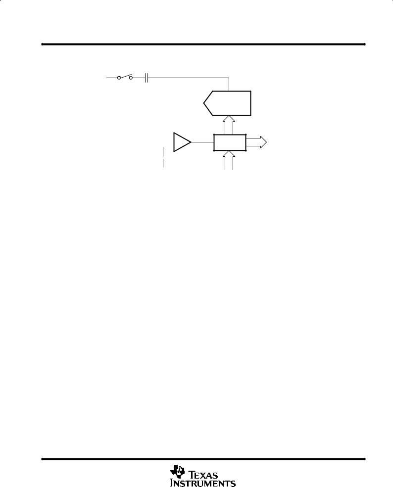
analog-to-digital SAR converter
Ain
|
|
|
|
|
|
|
|
Charge |
|
|
|
|
|
|
|
|
|
Redistribution |
|
||
|
|
|
|
|
|
|
|
|||
|
|
|
|
|
|
|
|
DAC |
|
|
|
|
|
|
|
|
_ |
|
|
|
|
|
|
|
|
|
|
|
SAR |
|
ADC Code |
|
|
|
|
|
|
|
|
|
|
||
|
|
|
|
|
|
+ |
|
Register |
|
|
|
|
|
|
|
|
|
|
|
||
|
|
|
|
|
|
|
|
|
|
|
|
|
|
|
|
|
|
|
|
|
|
|
|
|
|
|
|
|
|
|
||
|
|
|
|
|
|
|
|
|
|
|
REFM |
|
|
|
|
|
|||||
|
|
Control |
|
|
||||||
|
|
|
|
|
|
|
|
|
|
|
|
|
|
|
|
|
|
|
Logic |
|
|
|
|
|
|
|
|
|
|
|
|
|
Figure 1
The TLV571 is a successive-approximation ADC utilizing a charge redistribution DAC. Figure 1 shows a simplified version of the ADC.
The sampling capacitor acquires the signal on Ain during the sampling period. When the conversion process starts, the SAR control logic and charge redistribution DAC are used to add and subtract fixed amounts of charge from the sampling capacitor to bring the comparator into a balanced condition. When the comparator is balanced, the conversion is complete and the ADC output code is generated.
sampling frequency, fs
The TLV571 requires 16 CLKs for each conversion, therefore the equivalent maximum sampling frequency achievable with a given CLK frequency is:
fs(max) = (1/16) fCLK
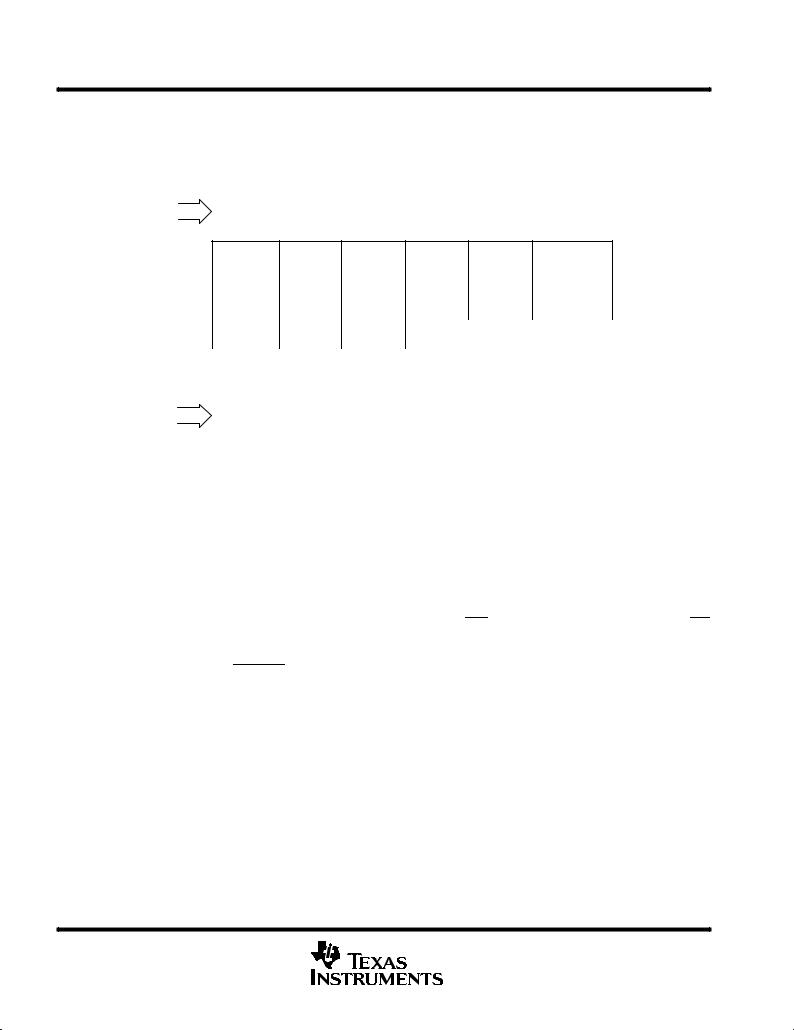
The TLV571 is software configurable. The first two MSB bits, D(7,6) are used to address which register to set. The remaining six bits are used as control data bits. There are two control registers, CR0 and CR1, that are user configurable. All of the register bits are written to the control register during write cycles. A description of the control registers is shown in Figure 2.
POST OFFICE BOX 655303 •DALLAS, TEXAS 75265 |
3 |
TLV571
2.7 V TO 5.5 V, 1-CHANNEL, 8-BIT,
PARALLEL ANALOG-TO-DIGITAL CONVERTER
SLAS239A ± SEPTEMBER 1999 ± REVISED FEBRUARY 2000
detailed description (continued)
control registers
A1 |
|
A0 |
D5 |
D4 |
D3 |
D2 |
D1 |
D0 |
|
|
|
|
Control Register Zero (CR0) |
|
|
|
|||
|
|
|
D5 |
D4 |
D3 |
D2 |
D1 |
D0 |
|
A(1:0)=00 |
|||||||||
STARTSEL |
PROGEOC |
CLKSEL |
SWPWDN |
Don't Care |
Don't Care |
||||
|
|
|
|||||||
0:0: 0: 0:
|
|
HARDWARE INT |
Internal |
NORMAL |
|
|
||
|
|
START |
|
Clock |
|
Don't Care |
Don't Care |
|
|
|
(CSTART) |
1: |
|
1: |
|||
|
|
|
|
|
||||
|
|
1: |
EOC |
1: |
Powerdown |
|
||
|
|
|
|
|
|
|||
|
|
SOFTWARE |
|
External |
|
|
|
|
|
|
|
|
|
|
|||
|
|
START |
|
Clock |
|
|
|
|
|
|
|
|
|
|
|
|
|
|
|
Control Register One (CR1) |
|
|
|
|||
|
|
D5 |
D4 |
D3 |
D2 |
D1 |
D0 |
|
A(1:0)=01 |
||||||||
Reserved |
OSCSPD |
0 Reserved |
0 Reserved |
OUTCODE |
Reserved |
|||
|
|
|||||||
|
|
|||||||
|
|
|
|
|
|
|
|
|
|
|
0: |
0: |
0: |
0: |
0: |
0: |
|
|
|
Reserved |
INT. OSC. |
Reserved |
Reserved |
Binary |
Reserved |
|
|
|
Bit |
SLOW |
Bit |
Bit, |
|
Bit, |
|
|
|
Always |
1: |
Always |
Always |
1: |
Always |
|
|
|
Write 0 |
INT. OSC. |
Write 0 |
Write 0 |
Write 0 |
||
|
|
|
FAST |
|
|
2's |
|
|
|
|
|
|
|
|
Complement |
|
|
|
|
|
|
|
|
|
||
|
|
|
|
|
|
|
|
|
Figure 2. Input Data Format
hardware configuration option
The TLV571 can configure itself. This option is enabled when the WR pin is tied to ground and a dummy RD signal is applied. The ADC is now fully configured. Zeros or default values are applied to both control registers. The ADC is configured ideally for 3-V operation, which means the internal OSC is set at 10 MHz and hardware start of conversion using CSTART.
ADC conversion modes
The TLV571 provides two start of conversion modes. Table 1 explains these modes in more detail.
4 |
POST OFFICE BOX 655303 •DALLAS, TEXAS 75265 |

|
|
|
|
|
|
TLV571 |
|||
|
2.7 V TO 5.5 V, 1-CHANNEL, 8-BIT, |
||||||||
|
PARALLEL ANALOG-TO-DIGITAL CONVERTER |
||||||||
|
SLAS239A ± SEPTEMBER 1999 ± REVISED FEBRUARY 2000 |
||||||||
|
|
|
|
|
|
|
|
|
|
detailed description (continued) |
|
|
|
|
|
|
|
|
|
|
Table 1. Conversion Modes |
|
|
|
|
|
|
|
|
|
|
|
|
|
|
|
|
|
|
START OF |
OPERATION |
|
COMMENTS ± FOR INPUT |
|
|||||
CONVERSION |
|
|
|||||||
|
|
|
|
|
|
|
|
|
|
|
|
|
|
|
|
|
|
|
|
Hardware start |
• Repeated conversions from AIN |
|
|
|
|
|
|
||
|
CSTART |
rising edge must be applied |
|
||||||
(CSTART) |
• CSTART falling edge to start sampling |
a minimum of 5 ns before or after CLK |
|
||||||
CR0.D5 = 0 |
• CSTART rising edge to start conversion |
rising edge. |
|
||||||
|
• If in INT mode, one INT pulse generated after each conversion |
|
|
|
|
|
|
|
|
|
• If in EOC mode, EOC will go high to low at start of conversion, and return high |
|
|
|
|
|
|
|
|
|
at end of conversion. |
|
|
|
|
|
|
|
|
|
|
|
|
|
|
|
|
||
|
• Repeated conversions from AIN |
|
|
|
|
||||
Software start |
With external clock, |
WR |
and |
RD |
rising |
|
|||
CR0.D5 = 1 |
• WR rising edge to start sampling initially. Thereafter, sampling occurs at the |
edge must be a minimum 5 ns before |
|
||||||
|
rising edge of RD. |
or after CLK rising edge. |
|
||||||
|
• Conversion begins after 6 clocks after sampling has begun. Thereafter, if in INT |
|
|
|
|
|
|
|
|
|
mode, one INT pulse generated after each conversion |
|
|
|
|
|
|
|
|
|
• If in EOC mode, EOC will go high to low at start of conversion and return high at |
|
|
|
|
|
|
|
|
|
end of conversion. |
|
|
|
|
|
|
|
|
|
|
|
|
|
|
|
|
|
|
configure the device
The device can be configured by writing to control registers CR0 and CR1.
Table 2. TLV571 Programming Examples
REGISTER |
|
INDEX |
D5 |
D4 |
D3 |
D2 |
D1 |
D0 |
COMMENT |
|
|
|
|
||||||||
D7 |
|
D6 |
||||||||
|
|
|
|
|
|
|
|
|
||
|
|
|
|
|
|
|
|
|
|
|
EXAMPLE1 |
|
|
|
|
|
|
|
|
|
|
|
|
|
|
|
|
|
|
|
|
|
CR0 |
0 |
|
0 |
0 |
0 |
0 |
0 |
0 |
0 |
Normal, INT OSC |
|
|
|
|
|
|
|
|
|
|
|
CR1 |
0 |
|
1 |
0 |
0 |
0 |
0 |
0 |
0 |
Binary |
|
|
|
|
|
|
|
|
|
|
|
EXAMPLE2 |
|
|
|
|
|
|
|
|
|
|
|
|
|
|
|
|
|
|
|
|
|
CR0 |
0 |
|
0 |
0 |
1 |
1 |
1 |
0 |
0 |
Power down, EXT OSC |
|
|
|
|
|
|
|
|
|
|
|
CR1 |
0 |
|
1 |
0 |
0 |
0 |
0 |
1 |
0 |
2's complement output |
power down
The TLV571 offers two power down modes, auto power down and software power down. This device will automatically proceed to auto power down mode if RD is not present one clock after conversion. Software power down is controlled directly by the user by pulling CS to DVDD.
Table 3. Power Down Modes
PARAMETERS/MODES |
AUTO POWER DOWN |
SOFTWARE POWER DOWN |
|
(CS = DVDD) |
|||
|
|
||
Maximum power down dissipation current |
1 mA |
10 A |
|
|
|
|
|
Comparator |
Power down |
Power down |
|
|
|
|
|
Clock buffer |
Power down |
Power down |
|
|
|
|
|
Control registers |
Saved |
Saved |
|
|
|
|
|
Minimum power down time |
1 CLK |
2 CLK |
|
|
|
|
|
Minimum resume time |
1 CLK |
2 CLK |
POST OFFICE BOX 655303 •DALLAS, TEXAS 75265 |
5 |
TLV571
2.7 V TO 5.5 V, 1-CHANNEL, 8-BIT,
PARALLEL ANALOG-TO-DIGITAL CONVERTER
SLAS239A ± SEPTEMBER 1999 ± REVISED FEBRUARY 2000
detailed description (continued)
reference voltage input
The TLV571 has two reference input pins: REFP and REFM. The voltage levels applied to these pins establish the upper and lower limits of the analog inputs to produce a full-scale and zero-scale reading respectively. The values of REFP, REFM, and the analog input should not exceed the positive supply or be less than GND consistent with the specified absolute maximum ratings. The digital output is at full scale when the input signal is equal to or higher than REFP and is at zero when the input signal is equal to or lower than REFM.
sampling/conversion
All sampling, conversion, and data output in the device are started by a trigger. This could be the RD, WR, or CSTART signal depending on the mode of conversion and configuration. The rising edge of RD, WR, and CSTART signal are extremely important, since they are used to start the conversion. These edges need to stay close to the rising edge of the external clock (if it is used as CLK). The minimum setup and hold time with respect to the rising edge of the external clock should be 5 ns minimum. When the internal clock is used, this is not an issue since these two edges will start the internal clock automatically. Therefore, the setup time is always met. Software controlled sampling lasts 6 clock cycles. This is done via the CLK input or the internal oscillator if enabled. The input clock frequency can be 1 MHz to 20 MHz, translating into a sampling time from 0.6 s to 0.3 s. The internal oscillator frequency is 9 MHz minimum (ocillator frequency is between 9 MHz to 22 MHz), translating into a sampling time from 0.6 s to 0.3 s. Conversion begins immediately after sampling and lasts 10 clock cycles. This is again done using the external clock input (1 MHz±20 MHz) or the internal oscillator (9 MHz minimum) if enabled. Hardware controlled sampling, via CSTART, begins on falling CSTART lasts the length of the active CSTART signal. This allows more control over the sampling time, which is useful when sampling sources with large output impedances. On rising CSTART, conversion begins. Conversion in hardware controlled mode also lasts 10 clock cycles. This is done using the external clock input (1 MHz±20 MHz) or the internal oscillator (9 MHz minimum) as is the case in software controlled mode.
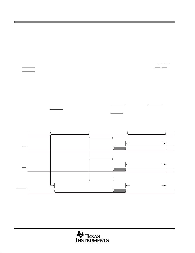
ExtClk
WR
RD
|
th(WRL_EXTCLKH) ≥ 5 ns |
|
tsu(WRH_EXTCLKH) ≥ 5 ns |
OR |
th(RDL_EXTCLKH) ≥ 5 ns |
|
|
|
tsu(RDH_EXTCLKH) ≥ 5 ns |
OR |
|
|
th(CSTARTL_EXTCLKH) ≥ 5 ns |
td(EXTCLK_CSTARTL) ≥ 5 ns |
tsu(CSTARTH_EXTCLKH) |
|
≥ 5 ns |
CSTART
NOTE: tsu = setup time, th = hold time
Figure 3. Trigger Timing ± Software Start Mode Using External Clock
6 |
POST OFFICE BOX 655303 •DALLAS, TEXAS 75265 |

TLV571 2.7 V TO 5.5 V, 1-CHANNEL, 8-BIT, PARALLEL ANALOG-TO-DIGITAL CONVERTER
SLAS239A ± SEPTEMBER 1999 ± REVISED FEBRUARY 2000
start of conversion mechanism
There are two ways to convert data: hardware and software. In the hardware conversion mode the ADC begins sampling at the falling edge of CSTART and begins conversion at the rising edge of CSTART. Software start mode ADC samples for 6 clocks, then conversion occurs for ten clocks. The total sampling and conversion process lasts only 16 clocks in this case. If RD is not detected during the next clock cycle, the ADC automatically proceeds to a power-down state. Data is valid on the rising edge of INT in both conversion modes.
hardware CSTART conversion
external clock
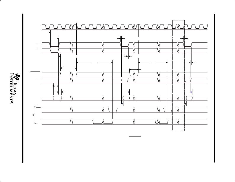
With CS low and WR low, data is written into the ADC. The sampling begins at the falling edge of CSTART and conversion begins at the rising edge of CSTART. At the end of conversion, EOC goes from low to high, telling the host that conversion is ready to be read out. The external clock is active and is used as the reference at all times. With this mode, it is required that CSTART is not applied at the rising edge of the clock (see Figure 4).
POST OFFICE BOX 655303 •DALLAS, TEXAS 75265 |
7 |
655303BOXOFFICEPOST•8 |
start of conversion mechanism (continued) |
|
2000FEBRUARYREVISED±1999SEPTEMBER±SLAS239A |
BIT-8CHANNEL,-1V,5.5toV7.2 CONVERTERDIGITAL-TO-ANALOGRARALLEL |
TLV571 |
|
|
|
|
|
|
||
|
CLK |
|
|
|
|
|
|
|
t su(CSL_WRL) |
|
|
|
|
|
|
t h(WRH_CSH) |
t su(CSL_RDL) |
t su(CSL_RDL) |
|
|
|
CS |
|
|
|
|
|
|
WR |
|
|
|
|
|
|
|
t d(CSH_CSTARTL) |
t h(RDH_CSH) |
|
|
|
|
|
tc |
|
tc |
|
|
|
|
(10 CLKs) |
|
|
|
|
|
|
t (sample) |
t(sample) |
|
|
|
|
|
|
|
|
|
|
|
CSTART |
|
|
|
|
|
|
RD |
|
|
|
|
|
|
|
t su(DAV_WRH) |
|
|
|
|
DALLAS, |
|
t h(WRH_DAV) |
t dis(RDH_DAV) |
|
|
|
D[0:7] |
Config |
ADC |
ADC |
|
|
|
TEXAS |
|
Data |
|
|
|
|
|
|
ten(RDL_DAV) |
t en(RDL_DAV) |
|
|
|
75265 |
|
|
|
|
||
INT |
|
|
|
|
|
|
|
|
|
|
|
|
|
|
OR |
|
|
|
|
|
|
EOC |
|
|
|
|
|
|
|
|
|
Auto Powerdown |
|
|
Figure 4. Input Conversion ± Hardware CSTART, External Clock

75265 TEXAS DALLAS, •655303 BOX OFFICE POST
9
internal clock
With CS low and WR low, data is written into the ADC. The sampling begins at the falling edge of CSTART, and conversion begins at the rising edge of CSTART. The internal clock turns on at the rising edge of CSTART. The internal clock is disabled after each conversion.
|
tsu(CSL_WRL) |
|
|
|
|
|
th(WRH_CSH) |
|
|
tsu(CSL_RDL) |
tsu(CSL_RDL) |
CS |
|
|
|
|
|
|
td(CSH_CSTARTL) |
|
|
|
|
WR |
|
|
|
|
|
|
|
|
|
|
t(STARTOSC) |
|
t(sample) |
|
|
th(RDH_CSH) |
tc |
CSTART |
|
|
|
|
|
|
0 |
1 |
9 |
10 |
|
INTCLK |
|
|
|
|
|
|
t(STARTOSC) |
|
|
||
RD |
|
|
|
|
|
|
tsu(DAV_WRH) |
|
|
|
|
|
th(WRH_DAV) |
|
|
tdis(RDH_DAV) |
|
D[0:7] |
Config |
|
|
ADC |
ADC |
|
Data |
|
|
Data |
Data |
|
|
|
|
ten(RDL_DAV) |
ten(RDL_DAV) |
INT |
|
|
|
|
|
OR |
|
|
tc |
|
|
|
|
|
|
|
|
EOC |
|
|
|
|
|
|
|
|
|
Auto Powerdown |
Auto Powerdown |
Figure 5. Input Conversion ± Hardware CSTART, Internal Clock
2000 FEBRUARY REVISED ± 1999 SEPTEMBER ± SLAS239A
TLV571 BIT-8 CHANNEL,-1 V, 5.5 TO V 7.2 CONVERTER DIGITAL-TO-ANALOG PARALLEL
 Loading...