


PROGRAMMABLE |
TMS279X |
PRODUCTS |
FLOPPY DISK FORMATTERICONTROLLER FAMILY |
|
JUNE 1984 |
∙On-Chip PILL Data Separator
∙On-Chip Write Precompensation Logic
∙Single + 5-V Supply
∙Accommodates Single-and Double-Density Formats
-MM3740 (FM)
-IBM34 (MFM)
∙Automatic Seek with Verify
∙Multiple Sector Read/Write
∙TTL Compatible
∙Programmable Control
-Selectable Track-to-Track Access
-Head Load Timing
∙Software Compatible with the FD179X Series
∙Soft Sector Format Compatibility
description
The TMS279X family are N-channel silicon gate MOS LSl devices which perform the functions of a Floppy Disk Formatter/Controller in a single chip implementation. The TMS279X, which can be considered the end result of both the Western Digital FD1771 and FD179X designs, is IBM compatible in single-density
FEATURES |
2791 |
2793 |
2795 |
2797 |
Single Density (FM) |
X |
X |
X |
X |
Double Density (MFM) |
X |
X |
X |
X |
True Data Bus |
|
X |
|
X |
Inverted Data Bus |
X |
|
X |
|
Side Select Out |
|
|
X |
X |
Internal CLK Divide |
X |
X |
|
|
mode (FM) and System 34 compatible in double-density mode (MFM). The TMS279X
contains all the features of its predecessor the FD179X plus a high performance phase-lock-loop data separator as well as write precompensation logic. In double-density mode, write precompensation is automatically engaged to a value programmed via an external potentiometer. In order to maintain compatibility, the FD1771, FD179X and TMS279X designs were made as close as possible with the computer interface, instruction set, and I/O registers being identical. Also, head load control is identical. In each case, the actual pin assignments vary by only a few pins from any one to another.
The processor interface consists of an 8-bit bi-directional bus for data, status, and control word transfers. The TMS279X is set up to operate on a multiplexed bus with other bus-oriented devices.
The TMS279X is TTL compatible on all inputs and outputs. The outputs will drive one TTL load or three LS loads. The 2793 is identical to the 2791 except the DAL lines are true for systems that utilize true data busses.
The 2795/7 has a side-select output for controlling double-sided drives.
Scanned and Edited by Michael Holley - Aug 21, 2001 - HolleyMJ@aol.com
Texas Instruments was a second source for the WD279X and this data sheet is almost identical to the Western Digital WD279X-02 Data Sheet and Application Note. (But has larger figures and is more readable.) Active low signals use a trailing # instead of an overbar.
TMS279X (WD279X) FLOPPY DISK FORMATTER / CONTROLLER FAMILY
pin descriptions
PIN |
PIN NAME |
SYMBOL |
|
|
|
FUNCTION |
|
NUMBER |
|
|
|
|
|
|
|
1 |
ENABLE PRECOMP |
ENP |
A Logic high on this input enables write precompensation to |
||||
|
|
|
be performed on double density Write Data output only. |
||||
19 |
MASTER RESET# |
MR# |
A logic low (50 microseconds min.) on this input resets the |
||||
|
|
|
device and loads HEX 03 into the command register. The Not |
||||
|
|
|
Ready (Status Bit 7) is reset during MR ACTIVE. When MR# |
||||
|
|
|
is brought to a logic high a RESTORE Command is executed, |
||||
|
|
|
regardless of the state of the Ready signal from the drive. |
||||
|
|
|
Also, HEX 01 is loaded into sector register. |
||||
|
POWER SUPPLIES |
VSS |
Ground |
|
|
|
|
20 |
|
|
|
|
|||
21 |
|
VCC |
+5V ±5% |
|
|
|
|
|
|
|
|
|
|
||
|
|
COMPUTER INERFACE |
|
|
|||
2 |
WRITE ENABLE# |
WE# |
A logic low on this input gates data on the DAL into the |
||||
|
|
|
selected register when CS# is low. |
|
|||
|
|
|
|
||||
3 |
CHIP SELECT# |
CS# |
A logic low on this input selects the chip and enables |
||||
|
|
|
computer communication with the device. |
||||
4 |
READ ENABLE# |
RE# |
A logic low on this input controls the placement of data from a |
||||
|
|
|
selected register on the DAL when CS# is low. |
||||
5,6 |
REGISTER SELECT |
A0, A1 |
These inputs select the register to receive / transfer data on |
||||
|
LINE |
|
the DAL lines under RE# and WE# control: |
||||
|
|
|
CS# |
A1 |
A0 |
RE# |
WE# |
|
|
|
0 |
0 |
0 |
Status Reg |
Command Reg |
|
|
|
0 |
0 |
1 |
Track Reg |
Track Reg |
|
|
|
0 |
1 |
0 |
Sector Reg |
Sector Reg |
|
|
|
0 |
1 |
1 |
Data Reg |
Data Reg |
7-14 |
DATA ACCESS LINES |
DALO- |
Eight bit bi-directional bus used for transfer of commands, |
||||
|
|
DAL7 |
status, and data. These lines are inverted (active low) on |
||||
|
|
|
TMS2791 and TMS2795. |
|
|||
24 |
CLOCK |
CLK |
This input requires a free-running 50% duty cycle square wave |
||||
|
|
|
clock for internal timing reference, 2 MHz ± 1 % for 8" drives, 1 |
||||
|
|
|
MHz ± 1 % for mini-floppies. |
|
|||
38 |
DATA REQUEST |
DRQ |
This output indicates that the Data Register contains |
||||
|
|
|
assembled data in Read operations, or the DR is empty in |
||||
|
|
|
Write operations. This signal is reset when serviced by the |
||||
|
|
|
computer through reading or loading the DR. |
||||
|
|
|
|
||||
39 |
INTERRUPT |
INTRQ |
This output is set at the completion of any command and is |
||||
|
REQUEST |
|
reset when the Status register is read or the Command |
||||
|
|
|
register is written to. |
|
|
||
|
|
|
|
|
|
||
|
|
FLOPPY DISK INTERFACE |
|
|
|||
15 |
STEP |
STEP |
The step output contains a pulse for each step. |
||||
16 |
DIRECTION |
DIRC |
Direction Output is active high when stepping in, active low |
||||
|
|
|
when stepping out. |
|
|
||
17 |
5 1/4”, 8" SELECT |
5#/8 |
This input selects the internal VCO frequency for use with |
||||
|
|
|
51/4" drives or 8" drives. |
|
|||
|
|
|
|
|
|
|
|
2
TMS279X (WD279X) FLOPPY DISK FORMATTER / CONTROLLER FAMILY
PIN |
PIN NAME |
SYMBOL |
FUNCTION |
|
NUMBER |
|
|
|
|
18 |
READ PULSE WIDTH |
RPW |
An external potentiometer tied to this input controls the phase |
|
|
|
|
comparator within the data separator. |
|
|
|
|
|
|
22 |
TEST# |
TEST# |
A logic low on this input allows adjustment of external resistors |
|
|
|
|
by enabling internal signals to appear on selected pins. |
|
23 |
PUMP |
PUMP |
High-Impedance output signal which is forced high or low to |
|
|
|
|
increase / decrease the VCO frequency |
|
25 |
ENABLE |
ENMF# |
A logic low on this input enables an internal divide by 2 of the |
|
|
MINI-FLOPPY |
|
Master Clock. This allows both 51/4" and 8" drive operation with |
|
|
(2791,2793) |
|
a single 2 MHz clock. For a 1 MHz clock on Pin 24, this line |
|
|
|
|
must be left open or tied to a Logic 1. |
|
25 |
SIDE SELECT |
SSO |
The logic level of the Side Select Output is directly controlled by |
|
|
OUTPUT |
|
the 'S' flag in Type 11 or III commands. When U = 1, SSO is set |
|
|
(2795,2797) |
|
to a logic 1. When U = 0, SSO is set to a logic 0. The SSO is |
|
|
|
|
compared with the compare Status Bit 4 (RNF) is set. The Side |
|
|
|
|
Select Output is only updated at the beginning of a Type II or III |
|
|
|
|
command. It is forced to a logic 0 upon a MASTER RESET |
|
|
|
|
condition. |
|
|
|
|
|
|
26 |
VOLTAGE- |
VCO |
An external capacitor tied to this pin adjusts the VCO center |
|
|
CONTROLLED |
|
frequency |
|
|
OSCILLATOR |
|
|
|
27 |
RAW READ# |
RAW RD# |
The data input signal directly from the drive. This input shall be |
|
|
|
|
a negative pulse for each recorded flux transition. |
|
28 |
HEAD LOAD |
HLD |
The HLD output controls the loading of the ReadWrite head |
|
|
|
|
against the media. |
|
29 |
TRACK GREATER |
TG43 |
This output informs the drive that the Read/Write head is |
|
|
||||
|
THAN 43 |
|
positioned between tracks 44-76. This output is valid only |
|
|
|
|
during Read and Write Commands. |
|
30 |
WRITE GATE |
WG |
This output is made valid before writing is to be performed on |
|
the diskette. |
||||
|
|
|
||
31 |
WRITE DATA |
WD |
MFM or FM output pulse per flux transition. WD contains the |
|
|
|
|
unique Address marks as well as data and clock in both FM and |
|
|
|
|
MFM formats. |
|
32 |
READY |
READY |
This input indicates disk readiness and is sampled for a logic |
|
|
|
|
high before Read or Write commands are performed. If Ready |
|
|
|
|
is low the Read or Write operation is not performed and an |
|
|
|
|
interrupt is generated. Type I operations are performed |
|
|
|
|
regardless of the state of Ready. The Ready input appears in |
|
|
|
|
inverted format as Status Register bit 7. |
|
33 |
WRITE PRECOMP |
WPW |
An external potentiometer tied to this input controls the amount |
|
|
WIDTH |
|
of delay in Write precompensation mode. |
|
34 |
TRACK 00# |
TR00# |
This input informs the TMS279X that the Read/Write head is |
|
|
|
|
positioned over Track 00. |
|
35 |
INDEX PULSE# |
IP# |
This input informs the TMS279X when the index hole is |
|
|
|
|
encountered on the diskette. |
|
36 |
WRITE PROTECT# |
WPRT# |
This input is sampled whenever a Write Command is received. |
|
A logic low terminates the command and sets the Write Protect |
||||
|
|
|
||
|
|
|
Status bit. |
|
NOTE: A trailing # replaces the overbar means the symbol is active low. |
||||
3
TMS279X (WD279X) FLOPPY DISK FORMATTER / CONTROLLER FAMILY
PIN |
PIN NAME |
SYMBOL |
FUNCTION |
NUMBER |
|
|
|
37 |
DOUBLE DENSITY# |
DDEN# |
This input pin selects either single or double density operation. |
|
|
|
When DDEN = 0, double density is selected. When DDEN = 1, |
|
|
|
single density is selected. |
40 |
HEAD LOAD TIMING |
HLT |
When a logic high is found on the HLT input the head is |
|
|
|
assumed to be engaged. It is typically derived from a 1 shot |
|
|
|
triggered by HLD. |
|
|
|
|
system interface
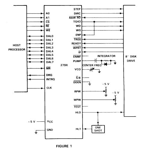
The TMS279X Floppy Disk Formatter/Controller system interface is shown in Figure 1. This interface consists of the parallel processor interface and the floppy disk interface. Applications for the TMS279X family are 8" floppy and 5 1/4" mini-floppy controller and singleor double-density controller/formatter.
The TMS279X family are MOS/LSI devices which perform the functions of a Floppy Disk Controller / Formatter. Software compatible with its predecessor, the FD179X the device also contains a high performance phase-lock-loop data separator as well as write precompensation logic.
When operating in double-density mode, write precompensation may be enabled, its value predetermined by an external potentiometer. An on-chip VCO and phase comparator allows adjustable frequency range for
5 1/4" or 8" floppy disk interfacing.
The TMS279X is fabricated in NMOS silicon gate technology and available in a 40-pin dual-in-line package.
4

TMS279X (WD279X) FLOPPY DISK FORMATTER / CONTROLLER FAMILY
functional block diagram
organization
The TMS279X is illustrated in the functional block diagram. The elements that comprise the TMS279X and the processor and floppy disk interface will be described in the paragraphs that follow.
data shift register
This 8-bit register assembles serial data from the read data input (RAW RD#) during read operations and transfers serial data to the write data output during write operations.
data register
This 8-bit register is used as a holding register during disk read and write operations. In disk read operations, the assembled data byte is transferred in parallel to the data register from the data shift register. In disk write operations, information is transferred in parallel from the data register to the data shift register.
5
TMS279X (WD279X) FLOPPY DISK FORMATTER / CONTROLLER FAMILY
When executing the Seek command, the data register holds 5e address of the desired track position. This register is loaded from the DAL and gated onto the DAL under processor control.
track register
This 8-bit register holds the track number of the current read/write head position. It is incremented by one every time the head is stepped in (towards track 76) and decremented by one when the head is stepped out (towards track 00). The contents of the register are compared with the recorded track number in the ID field during disk read, write and verify operations. The track register can be loaded from or transferred to the DAL. This register should not be loaded when the device is busy.
sector register (SR)
This 8-bit register holds the address of the desired sector position. The contents of the register are compared with the recorded sector number in the ID field during disk read or write operations. The sector register contents can be loaded from or transferred to the DAL. This register should not be loaded when the device is busy.
command register (CR)
This 8-bit register holds the command presently being executed. This register should not be loaded when the device is busy unless the new command is a force interrupt. The command register can be loaded from the DAL, but not read onto the DAL.
status register (STR)
This 8-bit register holds device status information. The meaning of the status bits is a function of the type of command previously executed. This register can be read onto the DAL, but not loaded from the DAL.
CRC logic
This logic is used to check or to generate the 16-bit cyclic redundancy check (CRC). The polynomial is: G(x) = x16 + x12 + x5 + 1.
The CRC includes all information starting with the address mark and up to the CRC characters. The CRC register is preset to ones prior to data being shifted through the circuit.
arithmetic/logic unit (ALU)
The ALU is a serial comparator, incrementer, and decrementer and is used for register modification and comparisons with the disk recorded ID field.
timing and control
All computer and floppy disk interface controls are generated through this logic. The internal device timing is generated from an external crystal clock.
AM detector
The address mark detector detects ID, data and index address marks during read and write operations.
write precompensation
Enables write precompensation to be performed on the double-density write data output.
data separator
A high-performance phase-lock-loop data separator with on-chip VCO and phase comparator allows adjustable frequency range for 5¼" or 8" floppy disk interfacing.
6
TMS279X (WD279X) FLOPPY DISK FORMATTER / CONTROLLER FAMILY
processor interface
The interface to the processor is accomplished through the eight data access lines (DAL) and associated control signals. The DAL are used to transfer data, status, and control words out of, or into the TMS279X. The DAL are three-state buffers that are enabled as output drivers when chip select (CS#) and read enable (RE#) are active (low logic state) or act as input receivers when CS# and write enable (WE#) are active.
When transfer of data with the floppy disk controller is required by the host processor, the device address is decoded and CS# is made low. The address bits A1 and AO, combined with the signals RE# during a mad operation or WE# during a write operation are interpreted as selecting the following registers:
A1 |
A0 |
READ (RE#) |
WRITE (WE#) |
|
|
|
|
0 |
0 |
Status Register |
Command Register |
0 |
1 |
Track Register |
Track Register |
1 |
0 |
Sector Register |
Sector Register |
1 |
1 |
Data Register |
Data Register |
|
|
|
|
During direct memory access (DMA) types of data transfers between the data register of the TMS279X and the processor, the data request (DRQ) output is used in data transfer control. This signal also appears as status bit 1 during read and write operations.
On disk read operations, the data request is activated (set high) when an assembled serial input byte is transferred in parallel to the data register. This bit is cleared when the data register is read by the processor. If the data register is read after one or more characters are lost, by having new data transferred into the register prior to processor readout, the lost data bit is set in the status register. The read operation continues until the end of sector is reached.
On disk write operations, the data request is activated when the data register transfers its contents to the data shift register, and requires a new data byte. It is reset when the data register is loaded with new data by the processor. If new data is not loaded at the time the next serial byte is required by the floppy disk, a byte of zeroes is written on the diskette and the lost data bit is set in the status register.
At the completion of every command, an INTRQ is generated. INTRQ is reset by either reading the status register or by loading the command register with a new command. In addition, INTRQ is generated if a Force Interrupt command condition is met.
The 279X has two modes of operation according to the state of DDEN# (pin 37). When DDEN# = 1, single density (FM) is selected. When DDEN# = 0, double density (MFM) is selected. In either case, the CLK input (pin 24) is set at 2 MHz for 8" drives or 1 MHz for 5 ¼" drives.
On the 2791/2793, the ENMF# input (pin 25) can be used for controlling both 5 ¼" and 8" drives with a single 2 MHz clock. When ENMF# = 0, an internal ÷ 2 of the CLK is performed. When ENMF# = 1, no divide takes place. This allows the use of a 2 MHz clock for both 5 ¼" and 8" configurations.
The internal VCO frequency must also be set to the proper value. The 5#/8 input (pin 17) is used to select data separator operation by internally dividing the read clock. When 5#/8 = 0, 5 ¼" data separation is selected; when 5#/8 = 1, 8 " drive data separation is selected.
CLOCK (24) |
ENMF# (25) |
5#/8 (17) |
DRIVE |
|
|
|
|
2 MHz |
1 |
1 |
8" |
2 MHz |
0 |
0 |
5 ¼" |
1 MHz |
0 |
0 |
5 ¼" |
|
|
|
|
7
TMS279X (WD279X) FLOPPY DISK FORMATTER / CONTROLLER FAMILY
functional description
The TMS279X-02 is software compatible with the FD179X-02 series of floppy disk controllers. Commands, status, and data transfers are performed in the same way. Software generated for the 179X can be transferred to a 279X system without modification.
In addition to the 179X, the 279X contains an internal data separator and write precompensation circuit. The TEST# (pin 22) line is used to adjust both data separator and precompensation. When TEST# = 0, the WD (pin 31) line is internally connected to the output of the write precomp one-shot. Adjustment of the WPW (pin 33) line can then be accomplished. A second one-shot tracks the precomp setting at approximately 3:1 to ensure adequate write data pulse durations to meet drive specifications.
Similarly, data separation is also adjusted with TEST# = 0. The TG43 (pin 2 9) line is internally connected to the output of the read data one-shot, which is adjusted via the R PW (pin 1811ine. The DIRC (pin 1611ine contains the read clock output (.5 MHz for 8" drives). The VCO trimming capacitor (pin 26) is adjusted for center frequency.
Internal timing signals are used to generate pulses during the adjustment mode so that these adjustments can be made while the device is in-circuit. The TEST# line also contains a pull-up resistor, so adjustments can b e performed simply by grounding the TEST# on, overriding the pull-up. The TEST# pin cannot be used to disable stepping rates during operation as its function is quite different from the 179X.
Other pins on the device also include pull-up resistors and may be left open to satisfy a logic 1 condition. These are: ENP, 5#/8, ENMF#, WPRT#, DDEN#, HLT, TEST#, and MR#.
general disk read operations
Sector lengths of 128, 256, 512 or 1024 are obtainable in either FM or MFM formats. For FM, DDEN# should be placed to logical "1." For MFM formats, DDEN# should be placed to a logical " 0." Sector lengths are determined at form at time by the fourth byte in the "ID" field.
SECTOR LENGTH TABLE*
SECTOR LENGTH |
NUMBER OF BYTES |
FIELD (HEX) |
IN SECTOR (DECIMAL) |
|
|
00 |
128 |
01 |
256 |
|
512 |
02 |
|
03 |
1024 |
|
|
*2795/97 may vary - see command summary.
The TMS279X recognizes tracks and sectors numbered 00-FFX.However, due to programming restrictions, only tracks and sectors 00 thru F4 can be formatted.
general disk write operation
When writing is to take place on the diskette, the write gate (WG) output is activated, allowing current to flow into the read/write head. As a precaution to erroneous writing, the first data byte must be loaded into the data register in response to a data request from the 279X before the write gate signal can be activated.
Writing is inhibited when the WRITE PROTECT# input is a logic low, in which case any Write command is immediately terminated, an interrupt is generated and the write protect status bit is set.
For write operations, the 279X provides write gate (pin 30) and write data (pin 31) outputs. Write data consists of a series of pulses set to a width approximately three times greater than the precomp adjustment. Write data provides the unique address marks in both formats.
8
TMS279X (WD279X) FLOPPY DISK FORMATTER / CONTROLLER FAMILY
ready
Whenever a Read or Write command (Type II or III) is received, the 279X samples the ready input. If this input is logic low the command is not executed and an interrupt is generated. All Type I commands are performed regardless of the state of the ready input. Also, whenever a Type II or III command is received, the TG43 signal output is updated. TG43 may be tied to ENP to enable write precompensation on tracks 44-76.
command description
The TMS279X will accept eleven commands. Command words should only be loaded in the command register when the busy status bit is off (status bit 0). The one exception is the Force Interrupt command. Whenever a command is being executed, Be busy status bit is set. When a command is completed, an interrupt is generated and the busy status bit is reset. The status register indicates whether the completed command encountered an error or was fault free. For ease of discussion, commands are divided into four types. Commands and Types are summarized in Table 1.
TABLE 1 - COMMAND SUMMARY
|
|
|
COMMANDS FOR MODELS |
|
|
COMMANDS FOR 2795,2797 |
|
||||||||||
|
|
|
|
|
2791,2793 |
|
|
|
|
|
|
|
|
|
|
|
|
|
|
|
|
|
|
|
|
|
|
|
|
|
|
|
|
||
TYPE |
COMMAND |
|
|
|
BITS |
|
|
|
|
|
|
BITS |
|
|
|
||
|
|
7 |
6 |
5 |
4 |
3 |
2 |
1 |
0 |
7 |
6 |
5 |
4 |
3 |
2 |
1 |
0 |
|
|
|
|
|
|
|
|
|
|
|
|
|
|
|
|
|
|
I |
Restore |
0 |
0 |
0 |
0 |
h |
V |
r1 |
r0 |
0 |
0 |
0 |
0 |
h |
V |
r1 |
r0 |
I |
Seek |
0 |
0 |
0 |
1 |
h |
V |
r1 |
r0 |
0 |
0 |
0 |
1 |
h |
V |
r1 |
r0 |
I |
Step |
0 |
0 |
1 |
T |
h |
V |
r1 |
r0 |
0 |
0 |
1 |
T |
h |
V |
r1 |
r0 |
I |
Step-in |
0 |
1 |
0 |
T |
h |
V |
r1 |
r0 |
0 |
1 |
0 |
T |
h |
V |
r1 |
r0 |
I |
Step-out |
0 |
1 |
1 |
T |
h |
V |
r1 |
r0 |
0 |
1 |
1 |
T |
h |
V |
r1 |
r0 |
II |
Read Sector |
1 |
0 |
0 |
m |
S |
E |
C |
0 |
1 |
0 |
0 |
m |
L |
E |
U |
0 |
II |
Write Sector |
1 |
0 |
1 |
m |
S |
E |
C |
a0 |
1 |
0 |
1 |
m |
L |
E |
U |
a0 |
III |
Read Address |
1 |
1 |
0 |
0 |
0 |
E |
0 |
0 |
1 |
1 |
0 |
0 |
0 |
E |
U |
0 |
III |
Read Track |
1 |
1 |
1 |
0 |
0 |
E |
0 |
0 |
1 |
1 |
1 |
0 |
0 |
E |
U |
0 |
III |
Write Track |
1 |
1 |
1 |
1 |
0 |
E |
0 |
0 |
1 |
1 |
1 |
1 |
0 |
E |
U |
0 |
IV |
Force Interrupt |
|
1 |
0 |
1 |
I3 |
I2 |
I 1 |
10 |
|
1 |
0 |
1 |
I3 |
I2 |
I 1 |
10 |
1 |
1 |
||||||||||||||||
9
TMS279X (WD279X) FLOPPY DISK FORMATTER / CONTROLLER FAMILY
TABLE 2 - FLAG SUMMARY
COMMAND |
BIT |
DESCRIPTION |
|
|
|
|
|
|
TYPE |
NUMBER(S) |
|
|
|
|
|
|
|
I |
0, 1 |
r1 r0 = Stepping Motor Rate |
|
|
|
|
|
|
|
|
See Table 3 for Rate Summary |
|
|
|
|
|
|
I |
2 |
V = Track Number Verify Flag |
V = 0, No verify |
|
|
|
|
|
|
|
|
V = 1, Verify on destination track |
|
|
|||
I |
3 |
h = Head Load Flag |
h = 0, Unload head at beginning |
|
|
|||
|
|
|
h = 1, Load head at beginning |
|
|
|||
I |
4 |
T = Track Update Flag |
T = 0, No update |
|
|
|
|
|
|
|
|
T = 1, Update track register |
|
|
|||
II & III |
0 |
a0 = Data Address Mark |
a0 = 0, FB (DAM) |
|
|
|
|
|
|
|
|
a0 = 1, F8 (deleted DAM) |
|
|
|
||
II |
1 |
C = Side Compare Flag |
C = 0, Disable side compare |
|
|
|||
|
|
|
C = 1, Enable side compare |
|
|
|||
II & III |
1 |
U = Update SSO |
U = 0, Update SSO to 0 |
|
|
|
||
|
|
|
U = 1, Update SSO to 1 |
|
|
|
||
II & III |
2 |
E = 1 5 ms Delay |
E = 0, No. 15 ms delay |
|
|
|
||
|
|
|
E = 1, 15 ms delay (30 ms for 1 MHz) |
|||||
II |
3 |
S = Side Compare Flag |
S = 0, Compare for side 0 |
|
|
|||
|
|
|
S = 1, Compare for side 1 |
|
|
|||
II |
3 |
L = Sector Length Flag |
LBS's Sector Length in ID Field |
|
|
|||
|
|
|
|
00 |
01 |
10 |
11 |
|
|
|
|
L=0 |
256 |
512 |
1024 |
128 |
|
|
|
|
L=1 |
128 |
256 |
512 |
1024 |
|
II |
4 |
m = Multiple Record Flag |
m=0, Single record |
|
|
|
||
|
|
|
m=1, Multiple record |
|
|
|
||
IV |
0-3 |
Ix = Interrupt Condition Flags |
|
|
|
|
|
|
|
|
I0 = 1 Not Ready to Ready Transition |
|
|
|
|
|
|
|
|
I1 = 1 Ready To Not Ready Transition |
|
|
|
|
|
|
|
|
I2 = 1 Index Pulse |
|
|
|
|
|
|
|
|
I3 = 1 Immediate Interrupt, Requires A Reset* |
|
|
|
|
||
|
|
I3-I0 = 0 Terminate With No Interrupt (INTRQ) |
|
|
|
|
||
*See Type IV command for further information.
write precompensation
When operating in double density mode (DDEN = 0), the 279X has the capability of providing a user-defined precompensation value for write data. An external potentiometer (10 k?) tied to the WPW signal (pin 33) allows a setting of 100 to 300 ns from nominal.
Setting the write precomp value is accomplished by forcing the TEST# line (pin 22) to a logic 0. A stream of pulses can then be seen on the write data (pin 31) line. Adjust the WPW potentiometer for the desired pulse duration. This adjustment may be performed in-circuit since write gate (pin 30) is inactive while TEST# = 0.
10
TMS279X (WD279X) FLOPPY DISK FORMATTER / CONTROLLER FAMILY
data separation
The 279X can operate with either an external data separator or its own internal recovery circuits. The condition of the TEST# line (pin 22) in conjunction with MR# (pin 19) will select internal or external mode.
To program the 279X for an external VCO, a MR# pulse must be applied while TEST# = 0. A clock equivalent to eight times the data rate (e.g., 4.0 MHz for 8" double density) is applied to the VCO input (pin 26).The feedback reference voltage is available on the pump output (pin 23) for external integration to control the VCO. TEST# is returned to a logic 1 for normal operation. Note: to maintain this mode, TEST# must be held low whenever MR# is applied.
For internal VCO operation, the TEST# line must be high during the MR# pulse, then set to a logic 0 for the adjustment procedure.
A 50 k? potentiometer tied to the RPW input (pin 18) is used to set the internal read data pulse for proper phasing. With a scope on pin 29 (TG43), adjust the RPW pulse for 1/8 of the data rate (250 ns for 8" double density). An n external variable capacitor of 5-60 pF is tied to the VCO input (pin 26) for adjusting center frequency. With a frequency counter on pin 16 (DIRC), adjust the trimmer cap to yield the appropriate data rate (500 kHz for 8" double density). The DDEN# line must below while the 5#/8 line is held high or the adjustment times above will be doubled.
After adjustments have been made, the TEST# pin is returned to a logic 1 and the device is ready for operation. Adjustments may be made in-circuit since the DIRC and TG43 lines may toggle without affecting the drive.
The PUMP output (pin 23) consists of positive and negative pulses; their duration is equivalent to the phase difference of incoming data vs. VCO frequency. This signal is internally connected to the VCO input, but a filter is needed to connect these pulses to a slow moving DC voltage.
The internal phase-detector is unsymmetrical for a random distribution of data pulses by a factor or two, in favor of a PUMP UP condition. Therefore, it is desirable to have a PUMP DOWN twice as responsive to prevent run-away during a lock attempt.
A first-order lag-lead filter can be used at the PUMP output (pin 23). This filter controls the instantaneous response of the VCO to bit-shifted data (jitter) as well as the response to normal frequency shift, i.e., the lock-up time. A balance must be accomplished between the two conditions to inhibit overresponsiveness to jitter and to prevent an extremely wide lock-up response, leading to PUMP runaway. The filter affects these two reactions in mutually opposite directions.
The following filter circuit is recommended for 8" FM/MFM:
Since 5 1/4" drives operate at exactly one-half the data rate (250 Kb/sec) the above capacitor should be doubled to 0.2 µF or 0.22 µF.
type I commands
The Type I commands include the Restore, Seek, Step, Step-In, and Step-Out commands. Each of the Type I commands contains a rate field (r0r1), which determines the stepping motor rate as defined in Table 3.
11

TMS279X (WD279X) FLOPPY DISK FORMATTER / CONTROLLER FAMILY
A 2 µs (MFM) or 4 µs (FM) pulse is provided as an output to the drive. For every step pulse issued, the drive moves one track location in a direction determined by the direction output. The chip will step the drive in the same direction it last stepped unless the command changes the direction.
The direction signal is active high when stepping in and low when stepping out. The direction signal is valid before the first stepping pulse is generated.
The rates (shown in Table 3) can be applied to a step-direction motor through the device interface.
TABLE 3 - STEPPING RATES
|
CLK |
2 MHz |
1 MHz |
r1 |
r0 |
TEST# = 1 |
TEST# = 1 |
0 |
0 |
3 ms |
6 ms |
0 |
1 |
6 ms |
12 ms |
1 |
0 |
10 ms |
20 ms |
1 |
1 |
15 ms |
30 ms |
After the last directional step, an additional 15 milliseconds of head settling time takes place if the verify flag is set in Type I commands. Note that this time doubles to 30 ms for a 1 MHz clock. There is also a 15 ms head settling time if the E flag is set in any Type 11 or III command.
When a Seek, Step or Restore command is executed, an optional verification of read-write head position can be performed by setting bit 2 (V = 1) in the command word to a logic 1. The verification operation begins at the end of the 15 millisecond settling time after the head is loaded against the media. The track number from the first encountered ID field is compared against the contents of the track register. If the track numbers compare and the ID field cyclic redundancy check (CRC) is correct, the verify operation is complete and an INTRQ is generated with no errors. If there is a match but not a valid CRC, the CRC error status bit is set (status bit 3), and the next encountered ID field is read from the disk for the verification operation.
The TMS279X must find an ID field with correct track number and correct CRC within 5 revolutions of the media; otherwise the seek error is set and an INTRQ is generated. If V = 0, no verification is performed.
The head load (HLD) output controls the movement of the read/write head against the media. HLD is activated at the beginning of a Type I command if the h flag is set (h = 1), at the end of the Type I command if the verify flag (V = 1), or upon receipt of any Type II or III command. Once HLD is active it remains active until either a Type I command is received with (h = 0 and V = 0); or if the 279X is in an idle state (non-busy) and 15 index pulses have occurred.
Head load timing (HLT) is an input to the 279X which is used for the head engage time. When HLT = 1, the 279X assumes the head is completely engaged. The head engage time is typically 30 to 100 ms depending on drive. The low-to-high transition on HLD is typically used to fire a one shot. The output of the one shot is then used for HLT and supplied as an input to the 279X.
HLT (FROM ONE SHOT)
HEAD LOAD TIMING
12
 Loading...