


Texas Instruments TLV5633IPWR, TLV5633IDWR, TLV5633IPW, TLV5633CPWR, TLV5633IDW Datasheet
...TLV5633C, TLV5633I 2.7 V TO 5.5 V LOW POWER 12-BIT DIGITAL-TO-ANALOG CONVERTERS WITH INTERNAL REFERENCE AND POWER DOWN
SLAS190 ± MARCH 1999
D12-Bit Voltage Output DAC
DProgrammable Internal Reference
DProgrammable Settling Time vs Power
Consumption
1 s in Fast Mode
3.5s in Slow Mode
D8-Bit Controller Compatible Interface
DDifferential Nonlinearity . . . <0.5 LSB Typ
DVoltage Output Range . . . 2x the Reference Voltage
DMonotonic Over Temperature
applications
DW OR PW PACKAGE
(TOP VIEW)
D2 |
|
1 |
20 |
|
|
D1 |
||||
|
|
|
||||||||
D3 |
|
2 |
19 |
|
|
D0 |
||||
|
|
|
||||||||
D4 |
|
3 |
18 |
|
|
CS |
|
|
|
|
|
|
|
|
|
|
|
||||
D5 |
|
4 |
17 |
|
|
WE |
|
|
|
|
D6 |
|
5 |
16 |
|
|
|
|
|
|
|
|
|
|
LDAC |
|
||||||
D7 |
|
6 |
15 |
|
|
|
|
|
|
|
|
|
|
PWR |
|
|
|||||
A1 |
|
7 |
14 |
|
|
AGND |
||||
|
|
|
||||||||
A0 |
|
8 |
13 |
|
|
OUT |
||||
|
|
|
||||||||
SPD |
9 |
12 |
|
|
REF |
|||||
|
|
|||||||||
DVDD |
10 |
11 |
|
|
AVDD |
|||||
|
|
|||||||||
|
|
|
|
|||||||
DDigital Servo Control Loops
DDigital Offset and Gain Adjustment
DIndustrial Process Control
DMachine and Motion Control Devices
DMass Storage Devices
description
The TLV5633 is a 12-bit voltage output digital-to-analog converter (DAC) with an 8-bit microcontroller compatible parallel interface. The 8 LSBs, the 4 MSBs, and 5 control bits are written using three different addresses. Developed for a wide range of supply voltages, the TLV5633 can be operated from 2.7 V to 5.5 V.
The resistor string output voltage is buffered by a x2 gain rail-to-rail output buffer. The buffer features a Class A (slow mode: AB) output stage to improve stability and reduce settling time. The programmable settling time of the DAC allows the designer to optimize speed versus power dissipation. With its on-chip programmable precision voltage reference, the TLV5633 simplifies overall system design. Because of its ability to source up to 1 mA, the internal reference can also be used as a system reference. The settling time and the reference voltage can be chosen by a control register.
Implemented with a CMOS process, the device is designed for single supply operation from 2.7 V to 5.5 V. It is available in 20-pin SOIC and TSSOP packages in standard commercial and industrial temperature ranges.
AVAILABLE OPTIONS
|
PACKAGE |
|
|
TA |
|
|
|
SOIC |
|
TSSOP |
|
|
(DW) |
|
(PW) |
|
|
|
|
0°C to 70°C |
TLV5633CDW |
|
TLV5633CPW |
|
|
|
|
± 40°C to 85°C |
TLV5633IDW |
|
TLV5633IPW |
|
|
|
|
Please be aware that an important notice concerning availability, standard warranty, and use in critical applications of Texas Instruments semiconductor products and disclaimers thereto appears at the end of this data sheet.
PRODUCTION DATA information is current as of publication date. Products conform to specifications per the terms of Texas Instruments standard warranty. Production processing does not necessarily include testing of all parameters.
Copyright 1999, Texas Instruments Incorporated
POST OFFICE BOX 655303 •DALLAS, TEXAS 75265 |
1 |
TLV5633C, TLV5633I
2.7 V TO 5.5 V LOW POWER 12-BIT DIGITAL-TO-ANALOG CONVERTERS WITH INTERNAL REFERENCE AND POWER DOWN
SLAS190 ± MARCH 1999
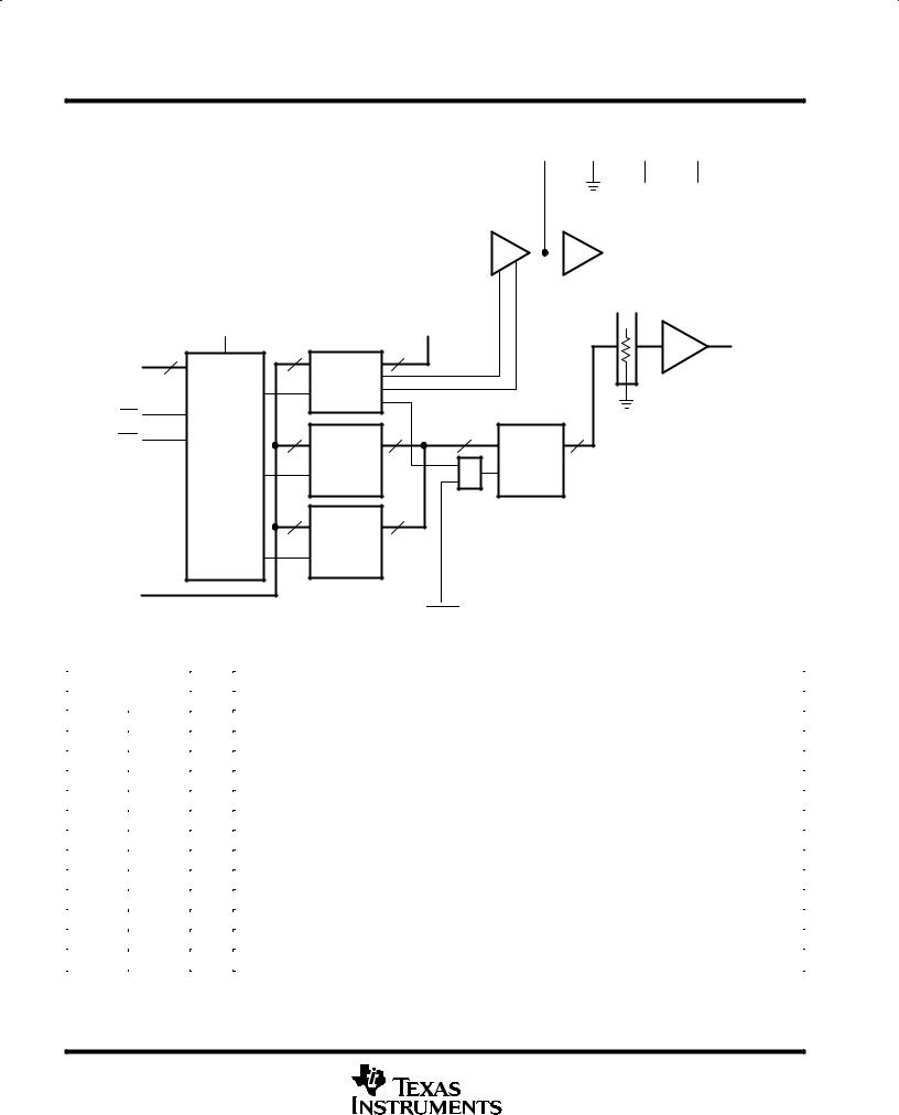
functional block diagram
REF AGND DVDD AVDD
PGA With
Output Enable
|
SPD |
|
|
|
|
|
|
Voltage |
|
|
|
||
|
|
|
Bandgap |
|
|
|
|||||||
|
|
|
|
|
|
|
|
|
|
|
|||
|
PWR |
|
|
|
|
|
|
|
|
|
|||
|
|
|
|
|
|
|
|
||||||
|
|
|
|
|
|
|
|
|
|
|
|
|
|
|
|
|
|
|
|
|
|
|
|
Powerdown |
|
|
|
|
|
|
|
|
Power-On |
|
|
|
|
and Speed |
|
|
|
|
|
|
|
|
|
|
|
|
|
|
|
||
|
|
|
|
|
Reset |
|
|
|
|
Control |
|
|
|
|
|
|
|
|
|
||||||||
|
|
|
|
|
|
|
|
|
|
|
|
|
|
|
2 |
5 |
|
2 |
|
x2 |
OUT |
|
|
|
|
|
|||
A(0,1) |
|
5-Bit |
|
|
|
|
|
|
|
|
|
|
|
||
|
|
|
Control |
|
|
|
|
|
|
Interface |
Latch |
|
|
|
|
CS |
|
|
|
|
|
|
|
|
Control |
|
|
|
|
|
|
WE |
|
4 |
4-Bit |
4 |
12 |
12 |
|
|
|
|
|
12-Bit |
|
||
|
|
|
DAC MSW |
|
|
DAC |
|
|
|
|
Holding |
|
|
|
|
|
|
|
|
|
Register |
|
|
|
|
|
Latch |
|
|
|
|
|
|
|
|
|
|
|
|
|
|
8 |
8-Bit |
8 |
|
|
|
|
|
|
|
|
|
|
|
|
|
|
DAC LSW |
|
|
|
|
|
|
|
Holding |
|
|
|
|
|
|
|
Latch |
|
|
|
|
D(0±7)
LDAC
|
|
|
|
|
|
|
|
Terminal Functions |
|
|
|
|
|
|
|
|
|
|
|
|
TERMINAL |
I/O/P |
DESCRIPTION |
|||
|
NAME |
NO. |
||||||
|
|
|
||||||
|
|
|
|
|
|
|
|
|
|
A1, A0 |
7, 8 |
I |
Address input |
||||
|
|
|
|
|
|
|
|
|
|
AGND |
14 |
P |
Ground |
||||
|
|
|
|
|
|
|
|
|
|
AVDD |
11 |
P |
Positive power supply (analog part) |
||||
|
|
|
|
|
|
18 |
I |
Chip select. Digital input active low, used to enable/disable inputs |
|
CS |
|
|
|
|
|||
|
D0 ± D1 |
19, 20 |
I |
Data input |
||||
|
|
|
|
|
|
|
|
|
|
D2 ± D7 |
1±6 |
I |
Data input |
||||
|
|
|
|
|
|
|
|
|
|
DVDD |
10 |
P |
Positive power supply (digital part) |
||||
|
|
|
|
|
|
16 |
I |
Load DAC. Digital input active low, used to load DAC output |
|
LDAC |
|
||||||
|
|
|
|
|
|
|
||
|
OUT |
13 |
O |
DAC analog voltage output |
||||
|
|
|
|
|
|
|||
|
|
|
|
|
|
15 |
I |
Power down. Digital input active low |
|
PWR |
|
||||||
|
|
|
|
|
|
|||
|
REF |
12 |
I/O |
Analog reference voltage input/output |
||||
|
|
|
|
|
|
|||
|
SPD |
9 |
I |
Speed select. Digital input |
||||
|
|
|
|
|
||||
|
|
|
|
|
|
17 |
I |
Write enable. Digital input active low, used to latch data |
|
WE |
|
||||||
|
|
|
|
|
|
|
|
|
2 |
POST OFFICE BOX 655303 •DALLAS, TEXAS 75265 |

TLV5633C, TLV5633I 2.7 V TO 5.5 V LOW POWER 12-BIT DIGITAL-TO-ANALOG CONVERTERS WITH INTERNAL REFERENCE AND POWER DOWN
SLAS190 ± MARCH 1999
absolute maximum ratings over operating free-air temperature range (unless otherwise noted)²
Supply voltage (DVDD, AVDD to AGND) . . . . . . . . . . . . . . . . . . . . . . . . . . . . . . . . . . . . . . |
. . . . . . . . . . . . . . . . . 7 |
V |
Supply voltage difference range, AVDD ± DVDD . . . . . . . . . . . . . . . . . . . . . . . . . . . . . . . . . |
. . . . . ± 2.8 V to 2.8 |
V |
Reference input voltage range . . . . . . . . . . . . . . . . . . . . . . . . . . . . . . . . . . . . . . . . . . . . . . . |
± 0.3 V to VDD + 0.3 |
V |
Digital input voltage range . . . . . . . . . . . . . . . . . . . . . . . . . . . . . . . . . . . . . . . . . . . . . . . . . . |
± 0.3 V to VDD + 0.3 |
V |
Operating free-air temperature range, TA: TLV5633C . . . . . . . . . . . . . . . . . . . . . . . . . . . . |
. . . . . . . . 0°C to 70°C |
|
TLV5633I . . . . . . . . . . . . . . . . . . . . . . . . . . . . . |
. . . . . . ±40°C to 85°C |
|
Storage temperature range, Tstg . . . . . . . . . . . . . . . . . . . . . . . . . . . . . . . . . . . . . . . . . . . . . . |
. . . . . ±65°C to 150°C |
|
Lead temperature 1,6 mm (1/16 inch) from case for 10 seconds . . . . . . . . . . . . . . . . . . |
. . . . . . . . . . . . . 260°C |
|
²Stresses beyond those listed under ªabsolute maximum ratingsº may cause permanent damage to the device. These are stress ratings only, and functional operation of the device at these or any other conditions beyond those indicated under ªrecommended operating conditionsº is not implied. Exposure to absolute-maximum-rated conditions for extended periods may affect device reliability.
recommended operating conditions
|
|
MIN |
NOM |
MAX |
UNIT |
|
|
|
|
|
|
|
|
Supply voltage, DVDD, AVDD |
5-V operation |
4.5 |
5 |
5.5 |
V |
|
|
|
|
|
|
||
3-V operation |
2.7 |
3 |
3.3 |
V |
||
|
||||||
|
|
|
|
|
|
|
Supply voltage difference, VDD = AVDD ± DVDD |
|
0 |
0 |
0 |
V |
|
Power on reset voltage, POR |
|
0.55 |
|
2 |
V |
|
|
|
|
|
|
|
|
High-level digital input voltage, VIH |
|
2 |
DVDD |
|
V |
|
Low-level digital input voltage, VIL |
|
|
0 |
0.8 |
V |
|
Reference voltage, Vref to REF terminal (5-V supply), See Note 1 |
|
AGND |
2.048 |
AVDD ±1.5 |
V |
|
Reference voltage, Vref to REF terminal (3-V supply), See Note 1 |
|
AGND |
1.024 |
AVDD ± 1.5 |
V |
|
Load resistance, RL |
|
2 |
|
|
kΩ |
|
Load capacitance, CL |
|
|
|
100 |
pF |
|
Operating free-air temperature, TA |
TLV5633C |
0 |
|
70 |
°C |
|
|
|
|
|
|||
TLV5633I |
± 40 |
|
85 |
|||
|
|
|
||||
|
|
|
|
|
|
NOTE 1: Due to the x2 output buffer, a reference input voltage ≥ AVDD/2 causes clipping of the transfer function. The output buffer of the internal reference must be disabled, if an external reference is used.
POST OFFICE BOX 655303 •DALLAS, TEXAS 75265 |
3 |

TLV5633C, TLV5633I
2.7 V TO 5.5 V LOW POWER 12-BIT DIGITAL-TO-ANALOG CONVERTERS WITH INTERNAL REFERENCE AND POWER DOWN
SLAS190 ± MARCH 1999
electrical characteristics over recommended operating free-air temperature range, Vref = 2.048 V, Vref = 1.024 V (unless otherwise noted)
power supply
|
PARAMETER |
|
TEST CONDITIONS |
|
MIN |
TYP |
MAX |
UNIT |
||||
|
|
|
|
|
|
|
|
|
|
|
|
|
|
|
|
|
|
|
|
REF on |
Fast |
|
2.3 |
2.8 |
mA |
|
|
|
|
|
|
|
|
|
|
|
|
|
|
|
|
|
|
|
AVDD = 5 V, |
Slow |
|
1.3 |
1.6 |
mA |
|
|
|
|
|
|
|
|
|
|||||
|
|
|
|
|
|
DVDD = 5 V |
REF off |
Fast |
|
1.9 |
2.4 |
mA |
|
|
No load, |
|
|
|
|
|
|
|
|
|
|
|
|
|
|
|
|
Slow |
|
0.9 |
1.2 |
mA |
||
|
|
|
|
|
|
|
|
|||||
IDD |
Power supply current |
All inputs = AGND or DVDD, |
|
|
|
|
||||||
|
|
|
|
|
|
|
|
|||||
|
|
|
Fast |
|
2.1 |
2.6 |
mA |
|||||
|
|
DAC latch = 0x800 |
|
|
|
|
REF on |
|
||||
|
|
|
|
|
|
|
|
|
|
|
||
|
|
|
|
|
|
AVDD = 3 V, |
Slow |
|
1.2 |
1.5 |
mA |
|
|
|
|
|
|
|
|
|
|||||
|
|
|
|
|
|
DVDD = 3 V |
REF off |
Fast |
|
1.8 |
2.3 |
mA |
|
|
|
|
|
|
|
Slow |
|
0.9 |
1.1 |
mA |
|
|
|
|
|
|
|
|
|
|
||||
|
|
|
|
|
|
|
|
|
|
|
|
|
|
Power down supply current |
|
|
|
|
|
|
|
|
0.01 |
1 |
µA |
|
|
|
|
|
|
|
|
|
|
|||
PSRR |
Power supply rejection ratio |
Zero scale, external reference, |
See Note 2 |
|
|
±60 |
|
dB |
||||
|
|
|
|
|
|
|
|
|
|
|||
Full scale, external reference, |
See Note 3 |
|
|
±60 |
|
|||||||
|
|
|
|
|
|
|||||||
NOTES: 2. Power supply rejection ratio at zero scale is measured by varying AVDD and is given by: |
|
|
|
|
||||||||
|
PSRR = 20 log [(EZS(AVDDmax) ± EZS(AVDDmin))/AVDDmax] |
|
|
|
|
|
||||||
|
3. Power supply rejection ratio at full scale is measured by varying AVDD and is given by: |
|
|
|
|
|||||||
|
PSRR = 20 log [(EG(AVDDmax) ± EG(AVDDmin))/AVDDmax] |
|
|
|
|
|
||||||
static DAC specifications |
|
|
|
|
|
|
|
|
|
|
|
|
|
|
|
|
|
|
|
|
|
|
|
|
|
|
PARAMETER |
|
|
|
|
TEST CONDITIONS |
|
MIN |
TYP |
MAX |
UNIT |
|
|
|
|
|
|
|
|
|
|
|
|
|
|
|
Resolution |
|
|
|
|
|
|
|
|
12 |
|
bits |
|
|
|
|
|
|
|
|
|||||
INL |
Integral nonlinearity, end point adjusted |
|
RL = 10 kΩ, CL = 100 pF, See Note 4 |
|
± 1.2 |
± 3 |
LSB |
|||||
DNL |
Differential nonlinearity |
|
|
RL = 10 kΩ, CL = 100 pF, See Note 5 |
|
± 0.3 |
± 0.5 |
LSB |
||||
EZS |
Zero-scale error (offset error at zero scale) |
|
See Note 6 |
|
|
|
± 12 |
mV |
||||
EZS TC |
Zero-scale-error temperature coefficient |
|
See Note 7 |
|
|
20 |
|
ppm/°C |
||||
EG |
Gain error |
|
|
See Note 8 |
|
|
|
± 0.3 |
% full |
|||
|
|
|
|
|
scale V |
|||||||
|
|
|
|
|
|
|
|
|
|
|
|
|
|
|
|
|
|
|
|
|
|
||||
EG TC |
Gain error temperature coefficient |
|
See Note 9 |
|
|
20 |
|
ppm/°C |
||||
NOTES: 4. The relative accuracy or integral nonlinearity (INL) sometimes referred to as linearity error, is the maximum deviation of the output from the line between zero and full scale excluding the effects of zero code and full-scale errors (see text).
5.The differential nonlinearity (DNL) sometimes referred to as differential error, is the difference between the measured and ideal 1 LSB amplitude change of any two adjacent codes. Monotonic means the output voltage changes in the same direction (or remains constant) as a change in the digital input code.
6.Zero-scale error is the deviation from zero voltage output when the digital input code is zero (see text).
7.Zero-scale-error temperature coefficient is given by: EZS TC = [EZS (Tmax) ± EZS (Tmin)]/2Vref × 106/(Tmax ± Tmin).
8.Gain error is the deviation from the ideal output (2Vref ± 1 LSB) with an output load of 10 kΩ excluding the effects of the zero-error.
9.Gain temperature coefficient is given by: EG TC = [EG(Tmax) ± EG (Tmin)]/2Vref × 106/(Tmax ± Tmin).
output specifications
|
PARAMETER |
TEST CONDITIONS |
MIN TYP |
MAX |
UNIT |
|
|
|
|
|
|
|
|
VO |
Output voltage |
RL = 10 kΩ |
|
|
AVDD±0.4 |
V |
|
Output load regulation accuracy |
VO = 4.096 V, 2.048 V, |
RL = 2 kΩ |
|
± 0.29 |
% full |
|
|
scale V |
||||
|
|
|
|
|
|
|
|
|
|
|
|
|
|
4 |
POST OFFICE BOX 655303 •DALLAS, TEXAS 75265 |

TLV5633C, TLV5633I 2.7 V TO 5.5 V LOW POWER 12-BIT DIGITAL-TO-ANALOG CONVERTERS WITH INTERNAL REFERENCE AND POWER DOWN
SLAS190 ± MARCH 1999
electrical characteristics over recommended operating free-air temperature range, Vref = 2.048 V, Vref = 1.024 V (unless otherwise noted) (Continued)
reference pin configured as output (REF)
|
PARAMETER |
TEST CONDITIONS |
MIN |
TYP |
MAX |
UNIT |
|
|
|
|
|
|
|
Vref(OUTL) |
Low reference voltage |
|
1.003 |
1.024 |
1.045 |
V |
Vref(OUTH) |
High reference voltage |
AVDD = DVDD > 4.75 V |
2.027 |
2.048 |
2.069 |
V |
Iref(source) |
Output source current |
|
|
|
1 |
mA |
Iref(sink) |
Output sink current |
|
±1 |
|
|
mA |
PSRR |
Power supply rejection ratio |
|
|
±48 |
|
dB |
reference pin configured as input (REF)
|
PARAMETER |
TEST CONDITIONS |
|
MIN |
TYP |
MAX |
UNIT |
|
|
|
|
|
|
|
|
|
|
VI |
Input voltage |
|
|
|
0 |
|
AVDD±1.5 |
V |
RI |
Input resistance |
|
|
|
|
10 |
|
MΩ |
CI |
Input capacitance |
|
|
|
|
5 |
|
pF |
|
Reference input bandwidth |
REF = 0.2 Vpp + 1.024 V dc |
Fast |
|
900 |
|
kHz |
|
|
|
|
|
|
||||
|
Slow |
|
500 |
|
||||
|
|
|
|
|
|
|
||
|
|
|
|
|
|
|
|
|
|
|
|
10 kHz |
Fast |
|
±87 |
|
dB |
|
|
|
|
|
|
|
||
|
Harmonic distortion, reference |
|
Slow |
|
±77 |
|
||
|
|
|
|
|
|
|||
|
REF = 1 Vpp + 2.048 V dc, AVDD = 5 V |
|
|
|
|
|
|
|
|
|
Fast |
|
±74 |
|
|
||
|
input |
50 kHz |
|
|
dB |
|||
|
|
Slow |
|
±61 |
|
|||
|
|
|
|
|
|
|
||
|
|
|
|
|
|
|
|
|
|
|
|
100 kHz |
Fast |
|
±66 |
|
dB |
|
|
|
|
|
|
|
|
|
|
Reference feedthrough |
REF = 1 Vpp at 1 kHz + 1.024 V dc (see Note 10) |
|
|
± 80 |
|
dB |
|
NOTE 10: Reference feedthrough is measured at the DAC output with an input code = 0x000. |
|
|
|
|
|
|||
digital inputs
|
PARAMETER |
TEST CONDITIONS |
MIN |
TYP |
MAX |
UNIT |
|
|
|
|
|
|
|
IIH |
High-level digital input current |
VI = DVDD |
|
|
1 |
µA |
IIL |
Low-level digital input current |
VI = 0 V |
±1 |
|
|
µA |
CI |
Input capacitance |
|
|
8 |
|
pF |
POST OFFICE BOX 655303 •DALLAS, TEXAS 75265 |
5 |

TLV5633C, TLV5633I
2.7 V TO 5.5 V LOW POWER 12-BIT DIGITAL-TO-ANALOG CONVERTERS WITH INTERNAL REFERENCE AND POWER DOWN
SLAS190 ± MARCH 1999
operating characteristics over recommended operating free-air temperature range, Vref = 2.048 V, and Vref = 1.024 V, (unless otherwise noted)
analog output dynamic performance
|
PARAMETER |
TEST CONDITIONS |
MIN |
TYP |
MAX |
UNIT |
|||
|
|
|
|
|
|
|
|
|
|
ts(FS) |
Output settling time, full scale |
RL = 10 kΩ, |
CL = 100 pF, |
|
Fast |
|
1 |
3 |
µs |
See Note 11 |
|
|
Slow |
|
3.5 |
7 |
|||
|
|
|
|
|
|
||||
|
|
|
|
|
|
|
|
|
|
ts(CC) |
Output settling time, code to code |
RL = 10 kΩ, |
CL = 100 pF, |
|
Fast |
|
0.5 |
1.5 |
µs |
See Note 12 |
|
|
Slow |
|
1 |
2 |
|||
|
|
|
|
|
|
||||
|
|
|
|
|
|
|
|
|
|
SR |
Slew rate |
RL = 10 kΩ, |
CL = 100 pF, |
|
Fast |
6 |
10 |
|
V/µs |
|
|
|
|
|
|||||
|
Slow |
1.2 |
1.7 |
|
|||||
|
|
See Note 13 |
|
|
|
|
|||
|
Glitch energy |
DIN = 0 to 1, |
fCLK = 100 kHz, |
|
5 |
|
nV±S |
||
|
CS = VDD |
|
|
|
|
|
|||
|
|
|
|
|
|
|
|
|
|
SNR |
Signal-to-noise ratio |
|
|
|
|
73 |
78 |
|
|
|
|
|
|
|
|
|
|
|
|
SINAD |
Signal-to-noise + distortion |
fs = 480 kSPS, |
fB = 20 kHz, |
fout = 1 kHz, |
61 |
67 |
|
dB |
|
THD |
Total harmonic distortion |
RL = 10 kΩ,, |
CL = 100 pF |
|
|
|
±69 |
±62 |
|
|
|
|
|
||||||
SFDR |
Spurious free dynamic range |
|
|
|
|
63 |
74 |
|
|
NOTES: 11. Settling time is the time for the output signal to remain within ± 0.5 LSB of the final measured value for a digital input code change of 0x020 to 0xFDF or 0xFDF to 0x020 respectively.
12.Settling time is the time for the output signal to remain within ± 0.5 LSB of the final measured value for a digital input code change of one count.
13.Slew rate determines the time it takes for a change of the DAC output from 10% to 90% full-scale voltage.
digital input timing requirements
|
|
|
|
|
|
|
|
|
|
|
|
|
|
|
|
|
|
|
|
MIN NOM MAX |
UNIT |
|
|
|
|
|
|
|
|
|
|
|
|
|
|
|
|
|
|
|
|
||
tsu(CS±WE) |
Setup time, |
|
|
|
low before negative |
|
|
|
edge |
15 |
ns |
||||||||||
CS |
|
|
WE |
||||||||||||||||||
tsu(D) |
Setup time, data ready before positive |
|
|
edge |
10 |
ns |
|||||||||||||||
WE |
|||||||||||||||||||||
tsu(A) |
Setup time, addresses ready before positive |
|
edge |
20 |
ns |
||||||||||||||||
WE |
|||||||||||||||||||||
th(DA) |
Hold time, data and addresses held valid after positive |
|
edge |
5 |
ns |
||||||||||||||||
WE |
|||||||||||||||||||||
|
|
|
|
|
|
|
|
|
|
||||||||||||
tsu(WE-LD) |
Setup time, positive |
WE |
edge before |
LDAC |
low |
5 |
ns |
||||||||||||||
|
|
|
|
|
|
||||||||||||||||
twH(WE) |
Pulse duration, |
WE |
high |
20 |
ns |
||||||||||||||||
tw(LD) |
Pulse duration, |
|
|
|
|
low |
23 |
ns |
|||||||||||||
LDAC |
|||||||||||||||||||||
6 |
POST OFFICE BOX 655303 •DALLAS, TEXAS 75265 |

TLV5633C, TLV5633I 2.7 V TO 5.5 V LOW POWER 12-BIT DIGITAL-TO-ANALOG CONVERTERS WITH INTERNAL REFERENCE AND POWER DOWN
SLAS190 ± MARCH 1999
PARAMETER MEASUREMENT INFORMATION
D(0±7) |
X |
|
|
Data |
X |
A(0,1) |
X |
|
Address |
X |
|
|
|
|
tsu(D) |
|
|
CS |
|
|
tsu(A) |
|
th(DA) |
|
|
|
|
|
|
|
|
tsu(CS-WE) |
|
twH(WE) |
|
WE |
|
|
|
|
|
|
|
|
|
tsu(WE-LD) |
tw(LD) |
LDAC |
|
|
|
|
|
|
|
|
Figure 1. Timing Diagram |
|
|
D(0±7) |
X |
MSW |
X |
LSW |
X |
A(0,1) |
X |
0 |
X |
1 |
X |
CS
WE
LDAC
Figure 2. Example of a Complete Write Cycle (MSW, LSW) Using LDAC for Update
POST OFFICE BOX 655303 •DALLAS, TEXAS 75265 |
7 |
 Loading...