


TLV2341, TLV2341Y LinCMOS PROGRAMMABLE LOW-VOLTAGE
OPERATIONAL AMPLIFIERS
SLOS110A ± MAY 1992 ± REVISED AUGUST 1994
DWide Range of Supply Voltages Over Specified Temperature Range:
TA = ±40°C to 85°C . . . 2 V to 8 V
DFully Characterized at 3 V and 5 V
DSingle-Supply Operation
DCommon-Mode Input-Voltage Range
Extends Below the Negative Rail and up to VDD ±1 V at 25°C
DHigh Input Impedance . . . 1012 Ω Typ
DLow Noise . . . 25 nV/√ Hz Typically at f = 1 kHz (High-Bias Mode)
DESD-Protection Circuitry
DDesigned-In Latch-Up Immunity
DBias-Select Feature Enables Maximum Supply Current Range From 17 μA to 1.5 mA at 25°C
DOutput Voltage Range Includes Negative Rail
D OR P PACKAGE |
PW PACKAGE |
(TOP VIEW) |
(TOP VIEW) |
OFFSET N1 |
|
1 |
8 |
|
BIAS SELECT |
OFFSET N1 |
|
|
1 |
8 |
|
|
BIAS SELECT |
|
|
|
|
|
|
||||||||
|
|
|
|
|
|
||||||||
IN± |
|
2 |
7 |
|
VDD |
IN± |
|
|
2 |
7 |
|
|
VDD |
|
|
|
|
3 |
6 |
|
|
||||||
IN+ |
|
3 |
6 |
|
OUT |
IN+ |
|
|
|
|
OUT |
||
|
|
4 |
5 |
|
|
||||||||
GND |
|
4 |
5 |
|
OFFSET N2 |
GND |
|
|
|
|
|
|
OFFSET N2 |
|
|
|
|
|
|
|
|||||||
|
|
|
|
|
|
|
|
|
|
|
|
|
|
description
The TLV2341 operational amplifier has been specifically developed for low-voltage, single-supply applications and is fully specified to operate over a voltage range of 2 V to 8 V. The device uses the Texas Instruments silicon-gate LinCMOS technology to facilitate low-power, low-voltage operation and excellent offset-voltage stability. LinCMOS technology also enables extremely high input impedance and low bias currents allowing direct interface to high-impedance sources.
The TLV2341 offers a bias-select feature, which allows the device to be programmed with a wide range of different supply currents and therefore different levels of ac performance. The supply current can be set at 17 μA, 250 μA, or 1.5 mA, which results in slew-rate specifications between 0.02 and 2.1 V/μs (at 3 V).
The TLV2341 operational amplifiers are especially well suited to single-supply applications and are fully specified and characterized at 3-V and 5-V power supplies. This low-voltage single-supply operation combined with low power consumption makes this device a good choice for remote, inaccessible, or portable battery-powered applications. The common-mode input range includes the negative rail.
The device inputs and outputs are designed to withstand ±100-mA currents without sustaining latch-up. The TLV2341 incorporates internal ESD-protection circuits that prevents functional failures at voltages up to 2000 V as tested under MIL-STD 883 C, Methods 3015.2; however, care should be exercised in handling these devices as exposure to ESD may result in the degradation of the device parametric performance.
AVAILABLE OPTIONS
|
|
|
PACKAGED DEVICES |
CHIP |
||
|
VIOmax |
|
|
|
|
|
|
SMALL |
|
PLASTIC |
|
||
TA |
|
TSSOP |
FORM |
|||
AT 25°C |
OUTLINE |
|
DIP |
|||
|
|
(PW) |
(Y) |
|||
|
|
(D) |
|
(P) |
||
|
|
|
|
|
||
|
|
|
|
|
|
|
± 40°C to 85°C |
8 mV |
TLV2341ID |
|
TLV2341IP |
TLV2341IPWLE |
TLV2341Y |
|
|
|
|
|
|
|
The D package is available taped and reeled. Add R suffix to the device type (e.g., TLV2341IDR).
The PW package is only available left-end taped and reeled (e.g., TLV2341IPWLE).
LinCMOS is a trademark of Texas Instruments Incorporated.
PRODUCTION DATA information is current as of publication date. Products conform to specifications per the terms of Texas Instruments standard warranty. Production processing does not necessarily include testing of all parameters.
Copyright 1994, Texas Instruments Incorporated
POST OFFICE BOX 655303 •DALLAS, TEXAS 75265 |
1 |
TLV2341, TLV2341Y
LinCMOS PROGRAMMABLE LOW-VOLTAGE
OPERATIONAL AMPLIFIERS
SLOS110A ± MAY 1992 ± REVISED AUGUST 1994
bias-select feature
The TLV2342 offers a bias-select feature that allows the user to select any one of three bias levels, depending on the level of performance desired. The tradeoffs between bias levels involve ac performance and power dissipation (see Table 1).
Table 1. Effect of Bias Selection on Performance
|
TYPICAL PARAMETER VALUES |
|
MODE |
|
|
|
|
|
|
|
|
UNIT |
|||
|
HIGH BIAS |
MEDIUM BIAS |
LOW BIAS |
||||
|
TA = 25°C, VDD = 3 V |
||||||
|
RL = 10 kΩ |
RL = 100 kΩ |
RL = 1 MΩ |
|
|
|
|
|
|
|
|
|
|||
PD |
Power dissipation |
975 |
195 |
15 |
μW |
||
SR |
Slew rate |
2.1 |
0.38 |
0.02 |
V/μs |
||
|
|
|
|
|
|
|
|
|
|
|
|
|
|
||
Vn |
Equivalent input noise voltage at f = 1 kHz |
25 |
32 |
68 |
nV/√ |
Hz |
|
B1 |
Unity-gain bandwidth |
790 |
300 |
27 |
kHz |
||
φm |
Phase margin |
46° |
39° |
34° |
|
|
|
AVD |
Large-signal differential voltage amplification |
11 |
83 |
400 |
V/mV |
||
bias selection
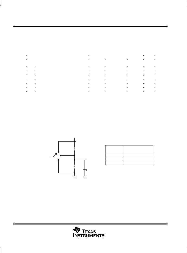
Bias selection is achieved by connecting BIAS SELECT to one of three voltage levels (see Figure 1). For medium-bias applications, it is recommended that the bias-select pin be connected to the midpoint between the supply rails. This procedure is simple in split-supply applications since this point is ground. In single-supply applications, the medium-bias mode necessitates using a voltage divider as indicated in Figure 1. The use of large-value resistors in the voltage divider reduces the current drain of the divider from the supply line. However, large-value resistors used in conjunction with a large-value capacitor require significant time to charge up to the supply midpoint after the supply is switched on. A voltage other than the midpoint may be used if it is within the voltages specified in the following table.
|
VDD |
|
|
|
Low |
1 MΩ |
BIAS MODE |
BIAS-SELECT VOLTAGE |
|
(single supply) |
||||
Medium |
|
|||
Low |
VDD |
|||
To the Bias-Select Pin |
|
|||
|
Medium |
1 V to VDD ± 1 V |
||
High |
|
|||
|
1 MΩ |
High |
GND |
|
|
|
|
||
|
|
0.01 μ F |
|
|
Figure 1. Bias Selection for Single-Supply Applications
2 |
POST OFFICE BOX 655303 •DALLAS, TEXAS 75265 |

TLV2341, TLV2341Y
LinCMOS PROGRAMMABLE LOW-VOLTAGE
OPERATIONAL AMPLIFIERS
SLOS110A ± MAY 1992 ± REVISED AUGUST 1994
high-bias mode
In the high-bias mode, the TLV2341 series feature low offset voltage drift, high input impedance, and low noise. Speed in this mode approaches that of BiFET devices but at only a fraction of the power dissipation.
medium-bias mode
The TLV2341 in the medium-bias mode features a low offset voltage drift, high input impedance, and low noise. Speed in this mode is similar to general-purpose bipolar devices but power dissipation is only a fraction of that consumed by bipolar devices.
low-bias mode
In the low-bias mode, the TLV2341 features low offset voltage drift, high input impedance, extremely low power consumption, and high differential voltage gain.
ORDER OF CONTENTS
TOPIC |
BIAS MODE |
|
|
|
|
Schematic |
all |
|
|
|
|
Absolute maximum ratings |
all |
|
|
|
|
Recommended operating conditions |
all |
|
|
|
|
Electrical characteristics |
high |
|
Operating characteristics |
||
(Figures 2 ± 31) |
||
Typical characteristics |
||
|
||
|
|
|
Electrical characteristics |
medium |
|
Operating characteristics |
||
(Figures 32 ± 61) |
||
Typical characteristics |
||
|
||
|
|
|
Electrical characteristics |
low |
|
Operating characteristics |
||
(Figures 62 ± 91) |
||
Typical characteristics |
||
|
||
|
|
|
Parameter measurement information |
all |
|
|
|
|
Application information |
all |
|
|
|
POST OFFICE BOX 655303 •DALLAS, TEXAS 75265 |
3 |
TLV2341, TLV2341Y
LinCMOS PROGRAMMABLE LOW-VOLTAGE
OPERATIONAL AMPLIFIERS
SLOS110A ± MAY 1992 ± REVISED AUGUST 1994
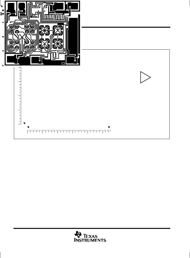
TLV2341Y chip information
This chip, when properly assembled, displays characteristics similar to the TLV2341. Thermal compression or ultrasonic bonding may be used on the doped-aluminum bonding pads. Chips may be mounted with conductive epoxy or a gold-silicon preform.
BONDING PAD ASSIGNMENTS
|
|
|
|
(2) |
(1) |
|
|
(8) |
(7) |
|
|
|
|
|
|
|
|
|
|
||
48 |
|
|
|
|
|
|
|
|||
|
(3) |
(4) |
(5) |
|
|
(6) |
||||
|
|
|
|
|||||||
|
|
|
|
|
|
|
||||
|
|
|
|
|
|
|
|
|
|
|
|
|
|
|
|
|
|
|
|
|
|
|
|
|
|
|
|
|
|
55 |
|
|
|
|
|
|
|
|
|
|
|
|
|
|
|
|
|
|
|
|
|
|
|
|
OFFSET N1 |
|
(1) |
|
|
VDD |
||||
|
|
(3) |
|
|
|
|
(7) |
|
|
IN + |
+ |
|
|
(6) |
|||||
|
|
|
|
||||||
|
|
||||||||
|
|
|
|||||||
IN ± |
(2) |
± |
|
|
|
|
OUT |
||
|
|
(4) |
|||||||
|
(5) |
|
|
|
|||||
OFFSET N2 |
|
|
|
|
|
||||
|
(8) |
|
|
GND |
|||||
BIAS SELECT |
|
|
|
|
|
|
|
||
|
|
|
|
|
|
|
|
|
|
|
|
|
|
|
|
|
|
|
|
CHIP THICKNESS: 15 TYPICAL BONDING PADS: 4 × 4 MINIMUM TJmax = 150°C
TOLERANCES ARE ± 10%.
ALL DIMENSIONS ARE IN MILS.
4 |
POST OFFICE BOX 655303 •DALLAS, TEXAS 75265 |

75265 TEXAS DALLAS, •655303 BOX OFFICE POST
5
equivalent schematic |
|
|
|
|
|
|
|
|
|
|
||
|
|
|
|
|
VDD |
|
|
|
|
|
|
|
|
|
P3 |
|
|
|
|
|
|
|
|
|
|
|
|
|
|
|
|
|
|
|
P12 |
|
|
|
|
|
|
|
|
|
|
|
P9A |
|
|
|
|
|
|
|
P4 |
R6 |
P5 |
|
P9B |
|
|
|
|
|
|
|
|
|
|
|
P11 |
|
|
|
|||
|
|
|
|
|
|
|
|
|
|
|
||
|
|
|
|
|
|
|
|
|
|
|
|
|
P1 |
|
P2 |
R2 |
|
|
|
|
|
|
|
|
|
IN ± |
|
|
|
|
|
|
|
|
|
|
|
|
R1 |
|
|
|
N5 |
|
|
|
|
P10 |
|
|
|
|
|
|
|
|
|
|
|
|
|
|
||
|
|
|
|
|
|
|
|
|
N11 |
|
|
|
IN + |
|
|
|
C1 |
P6A |
P6B |
P7B |
P7A |
P8 |
|
|
|
|
|
|
R5 |
|
|
|
||||||
|
|
|
|
|
|
|
|
|
|
|
||
|
|
|
N3 |
|
|
|
|
|
N12 |
|
LinCMOS |
|
|
|
|
|
|
|
N6 |
|
|
N9 |
|
|
|
|
|
|
|
|
|
|
|
|
|
|
||
|
|
|
|
|
|
|
|
|
|
|
|
|
|
|
|
|
|
|
|
|
|
N7 |
|
|
|
|
N1 |
N2 |
|
|
|
|
|
|
|
|
|
|
|
|
|
|
N4 |
|
|
|
|
1994AUGUSTREVISED±1992MAY±SLOS110A |
AMPLIFIERSOPERATIONAL |
VOLTAGE-LOWPROGRAMMABLE |
TLV2341YTLV2341, |
|
|
|
|
|
|
|
|
|
N13 |
|
|
|
R3 |
D1 |
R4 |
D2 |
|
|
R7 |
|
|
|
|
|
|
|
|
|
|
|
|
|
|
|
N10 |
|
|
|
|
OFFSET |
OFFSET |
|
|
OUT |
|
GND |
|
BIAS |
|
|
|
|
N1 |
N2 |
|
|
COMPONENT COUNT² |
|
|
SELECT |
|
|
|
|
|
|
|
|
|
|
|
|
|
|
|
||
|
|
|
|
|
Transistors |
27 |
|
|
|
|
|
|
|
|
|
|
|
Diodes |
2 |
|
|
|
|
|
|
|
|
|
|
|
Resistors |
7 |
|
|
|
|
|
|
|
|
|
|
|
Capacitors |
1 |
|
|
|
|
|
|
|
|
|
|
² Includes the amplifier and all |
|
|
|
|
|
|
||
|
|
|
|
|
ESD, bias, and trim circuitry |
|
|
|
|
|
|
|
TLV2341, TLV2341Y
LinCMOS PROGRAMMABLE LOW-VOLTAGE
OPERATIONAL AMPLIFIERS
SLOS110A ± MAY 1992 ± REVISED AUGUST 1994
absolute maximum ratings over operating free-air temperature range (unless otherwise noted)²
Supply voltage, VDD (see Note 1) . . . . . . . . . . . . . . . . . . . . . . . . . . . . . . . . . . . . . . . |
. . . . . . . . . . . . . . . . . . . . . . 8 V |
Differential input voltage (see Note 2) . . . . . . . . . . . . . . . . . . . . . . . . . . . . . . . . . . . . |
. . . . . . . . . . . . . . . . . . . . VDD ± |
Input voltage range, VI (any input) . . . . . . . . . . . . . . . . . . . . . . . . . . . . . . . . . . . . . . . |
. . . . . . . . . . . . ±0.3 V to VDD |
Input current, II . . . . . . . . . . . . . . . . . . . . . . . . . . . . . . . . . . . . . . . . . . . . . . . . . . . . . . . |
. . . . . . . . . . . . . . . . . . . ± 5 mA |
Output current, IO . . . . . . . . . . . . . . . . . . . . . . . . . . . . . . . . . . . . . . . . . . . . . . . . . . . . . |
. . . . . . . . . . . . . . . . . . ± 30 mA |
Duration of short-circuit current at (or below) TA = 25°C (see Note 3) . . . . . . . . |
. . . . . . . . . . . . . . . . . unlimited |
Continuous total dissipation . . . . . . . . . . . . . . . . . . . . . . . . . . . . . . . . . . . . . . . . . . . |
See Dissipation Rating Table |
Operating free-air temperature range, TA . . . . . . . . . . . . . . . . . . . . . . . . . . . . . . . . |
. . . . . . . . . . . . ±40°C to 85°C |
Storage temperature range . . . . . . . . . . . . . . . . . . . . . . . . . . . . . . . . . . . . . . . . . . . . . |
. . . . . . . . . . . ±65°C to 150°C |
Lead temperature 1,6 mm (1/16 inch) from case for 10 seconds . . . . . . . . . . . . |
. . . . . . . . . . . . . . . . . . . 260°C |
²Stresses beyond those listed under ªabsolute maximum ratingsº may cause permanent damage to the device. These are stress ratings only, and functional operation of the device at these or any conditions beyond those indicated under ªrecommended operating conditionsºsi not implied. Exposure to absolute-maximum-rated conditions for extended periods may effect device reliability.
NOTES: 1. All voltage values, except differential voltages, are with respect to network ground.
2.Differential voltages are at the noninverting input with respect to the inverting input.
3.The output may be shorted to either supply. Temperature and/or supply voltages must be limited to ensure that the maximum dissipation rating is not exceeded (see application section).
DISSIPATION RATING TABLE
PACKAGE |
TA ≤ 25°C |
DERATING FACTOR |
TA = 85°C |
|
POWER RATING |
ABOVE TA = 25°C |
POWER RATING |
||
|
||||
D |
725 mW |
5.8 mW/°C |
377 mW |
|
P |
1000 mW |
8.0 mW/°C |
520 mW |
|
PW |
525 mW |
4.2 mW/°C |
273 mW |
|
|
|
|
|
recommended operating conditions
|
|
MIN |
MAX |
UNIT |
|
|
|
|
|
|
|
Supply voltage, VDD |
|
2 |
8 |
V |
|
Common-mode input voltage, VIC |
VDD = 3 V |
± 0.2 |
1.8 |
V |
|
VDD = 5 V |
± 0.2 |
3.8 |
|||
|
|
||||
Operating free-air temperature, TA |
|
± 40 |
85 |
°C |
6 |
POST OFFICE BOX 655303 •DALLAS, TEXAS 75265 |
|
|
|
|
LinCMOS |
|
|
TLV2341, TLV2341Y |
||||||
|
|
|
|
PROGRAMMABLE LOW-VOLTAGE |
|||||||||
|
|
|
|
|
|
OPERATIONAL AMPLIFIERS |
|||||||
|
|
|
|
|
|
SLOS110A ± MAY 1992 ± REVISED AUGUST 1994 |
|||||||
|
|
|
|
|
|
|
|
|
|
|
|
|
|
|
|
|
HIGH-BIAS MODE |
|
|
|
|
|
|
|
|
||
electrical characteristics at specified free-air temperature |
|
|
|
|
|
|
|
|
|||||
|
|
|
|
|
|
|
|
|
|
|
|
|
|
|
|
|
TEST |
|
|
|
TLV2341I |
|
|
|
|
|
|
|
PARAMETER |
|
T ² |
|
|
|
|
|
|
|
UNIT |
|
|
|
|
V = 3 V |
|
V |
DD |
= 5 V |
|
|
|||||
|
|
|
|
|
|
||||||||
|
|
CONDITIONS |
A |
|
DD |
|
|
|
|
|
|
||
|
|
|
|
|
MIN |
TYP |
MAX |
MIN |
TYP |
MAX |
|
|
|
|
|
|
|
|
|
|
|
|
|
|
|
|
|
|
|
VO = 1 V, |
° |
|
0.6 |
8 |
|
|
1.1 |
8 |
|
|
|
|
|
VIC = 1 V, |
25 C |
|
|
|
|
|
|||||
VIO |
Input offset voltage |
|
|
|
|
|
|
|
|
mV |
|
||
RS |
= 50 Ω, |
Full range |
|
|
10 |
|
|
|
10 |
|
|||
|
|
|
|
|
|
|
|
|
|||||
|
|
RL = 10 kΩ |
|
|
|
|
|
|
|
||||
|
|
|
|
|
|
|
|
|
|
|
|
||
αVIO |
Average temperature of input |
|
|
25°C to |
|
2.7 |
|
|
|
2.7 |
|
μV/°C |
|
offset voltage |
|
|
85°C |
|
|
|
|
|
|
||||
|
|
|
|
|
|
|
|
|
|
|
|
||
|
|
|
|
|
|
|
|
|
|
|
|
|
|
IIO |
Input offset current (see Note 4) |
VO = 1 V, |
25°C |
|
0.1 |
|
|
|
0.1 |
|
pA |
|
|
|
|
|
|
|
|
|
|
|
|||||
V |
= 1 V |
° |
|
22 |
1000 |
|
|
24 |
1000 |
|
|||
|
|
IC |
|
85 C |
|
|
|
|
|
||||
IIB |
Input bias current (see Note 4) |
VO = 1 V, |
25°C |
|
0.6 |
|
|
|
0.6 |
|
pA |
|
|
|
|
|
|
|
|
|
|
|
|||||
V |
= 1 V |
° |
|
175 |
2000 |
|
|
200 |
2000 |
|
|||
|
|
IC |
|
85 C |
|
|
|
|
|
||||
|
|
|
|
25°C |
± 0.2 |
± 0.3 |
|
± 0.2 |
± 0.3 |
|
|
|
|
|
|
|
|
to |
to |
|
to |
|
to |
|
V |
|
|
VICR |
Common-mode input voltage range |
|
|
|
2 |
2.3 |
|
4 |
|
4.2 |
|
|
|
(see Note 5) |
|
|
|
± 0.2 |
|
|
± 0.2 |
|
|
|
|
|
|
|
|
|
|
|
|
|
|
|
|
|
|||
|
|
|
|
|
|
|
|
|
|
|
|
||
|
|
|
|
Full range |
to |
|
|
to |
|
|
|
V |
|
|
|
|
|
|
1.8 |
|
|
3.8 |
|
|
|
|
|
|
|
|
|
|
|
|
|
|
|
|
|
|
|
|
|
V |
= 1 V, |
° |
1.75 |
1.9 |
|
3.2 |
|
3.7 |
|
|
|
VOH |
High-level output voltage |
IC |
|
25 C |
|
|
|
V |
|
||||
VID = 100 mV, |
|
|
|
|
|
|
|
|
|
||||
Full range |
1.7 |
|
|
3 |
|
|
|
|
|||||
|
|
IOH = ± 1 mA |
|
|
|
|
|
|
|
||||
|
|
V |
= 1 V, |
° |
|
120 |
150 |
|
|
90 |
150 |
|
|
VOL |
Low-level output voltage |
IC |
|
25 C |
|
|
|
mV |
|
||||
VID = ±100 mV, |
|
|
|
|
|
|
|
|
|
||||
Full range |
|
|
190 |
|
|
|
190 |
|
|||||
|
|
IOL = 1 mA |
|
|
|
|
|
|
|
||||
|
|
V |
= 1 V, |
° |
3 |
11 |
|
5 |
|
23 |
|
|
|
|
Large-signal differential |
IC |
|
25 C |
|
|
|
|
|
||||
AVD |
RL |
= 10 kΩ, |
|
|
|
|
|
|
|
|
V/mV |
|
|
voltage amplification |
Full range |
2 |
|
|
3.5 |
|
|
|
|
||||
|
See Note 6 |
|
|
|
|
|
|
|
|||||
|
|
|
|
|
|
|
|
|
|||||
|
|
|
|
|
|
|
|
|
|
|
|
|
|
|
|
V |
= 1 V, |
° |
65 |
78 |
|
65 |
|
80 |
|
|
|
CMRR |
Common-mode rejection ratio |
O |
|
25 C |
|
|
|
dB |
|
||||
VIC = VICRmin, |
|
|
|
|
|
|
|
|
|
||||
Full range |
60 |
|
|
60 |
|
|
|
|
|||||
|
|
RS = 50 Ω |
|
|
|
|
|
|
|
||||
|
|
V |
= 1 V, |
° |
70 |
95 |
|
70 |
|
95 |
|
|
|
kSVR |
Supply-voltage rejection ratio |
IC |
|
25 C |
|
|
|
dB |
|
||||
VO |
= 1 V, |
|
|
|
|
|
|
|
|
|
|||
( VDD / VIO) |
Full range |
65 |
|
|
65 |
|
|
|
|
||||
|
RS |
= 50 Ω |
|
|
|
|
|
|
|
||||
|
|
|
|
|
|
|
|
|
|||||
II(SEL) |
Bias select current |
VI(SEL) = 0 |
25°C |
|
± 1.2 |
|
|
± 1.4 |
|
μA |
|
||
|
|
VO = 1 V, |
25°C |
|
325 |
1500 |
|
|
675 |
1600 |
μA |
|
|
IDD |
Supply current |
VIC = 1 V, |
|
|
|
|
|
|
|
|
|
||
Full range |
|
|
2000 |
|
|
|
2200 |
|
|||||
|
|
No load |
|
|
|
|
|
|
|
||||
|
|
|
|
|
|
|
|
|
|
|
|
|
|
² Full range is ± 40°C to 85°C.
NOTES: 4. The typical values of input bias current and input offset current below 5 pA are determined mathematically.
5.This range also applies to each input individually.
6.At VDD = 5 V, VO = 0.25 V to 2 V; at VDD = 3 V, VO = 0.5 V to 1.5 V.
POST OFFICE BOX 655303 •DALLAS, TEXAS 75265 |
7 |
TLV2341, TLV2341Y
LinCMOS PROGRAMMABLE LOW-VOLTAGE
OPERATIONAL AMPLIFIERS
SLOS110A ± MAY 1992 ± REVISED AUGUST 1994
HIGH-BIAS MODE
operating characteristics at specified free-air temperature, VDD = 3 V
|
PARAMETER |
|
|
TEST CONDITIONS |
TA |
|
TLV2341I |
|
UNIT |
||||
|
|
|
|
|
|
||||||||
|
|
|
MIN |
TYP |
MAX |
||||||||
|
|
|
|
|
|
|
|
|
|
|
|||
|
|
|
|
|
|
|
|
|
|
|
|
|
|
|
|
V |
|
= 1 V, |
V |
= 1 V, |
° |
|
2.1 |
|
|
|
|
|
|
IC |
I(PP) |
|
25 C |
|
|
|
|
|
|||
SR |
Slew rate at unity gain |
RL = 10 kΩ, |
CL = 20 pF, |
|
|
|
|
V/μs |
|||||
85°C |
|
1.7 |
|
||||||||||
|
|
See Figure 92 |
|
|
|
|
|
|
|
||||
|
|
|
|
|
|
|
|
|
|
|
|||
Vn |
Equivalent input noise voltage |
f = kHz, |
RS = 20 Ω, |
25°C |
|
25 |
|
|
|
|
|||
|
|
nV/√ Hz |
|||||||||||
See Figure 93 |
|
|
|
|
|||||||||
|
|
|
|
|
|
|
|
|
|
|
|||
|
|
|
|
|
|
|
|
|
|
|
|
|
|
BOM |
Maximum output-swing bandwidth |
VO = VOH, |
CL = 20 pF, |
25°C |
|
170 |
|
kHz |
|||||
|
|
|
|
||||||||||
R |
L |
= 10 kΩ, |
See Figure 92 |
° |
|
145 |
|
||||||
|
|
|
|
|
|
85 C |
|
|
|
|
|
||
B1 |
Unity-gain bandwidth |
VI = 10 mV, |
CL = 20 pF, |
25°C |
|
790 |
|
kHz |
|||||
|
|
|
|
||||||||||
R |
L |
= 10 kΩ, |
See Figure 94 |
° |
|
690 |
|
||||||
|
|
|
|
|
|
85 C |
|
|
|
|
|
||
|
|
VI = 10 mV, |
f = B1, |
|
± 40°C |
|
53° |
|
|
|
|
||
|
|
|
|
|
|
|
|
|
|
||||
φm |
Phase margin |
CL = 20 pF, |
RL = 1 MΩ, |
25°C |
|
49° |
|
|
|
|
|||
|
|
See Figure 94 |
|
|
85°C |
|
47° |
|
|
|
|
||
|
|
|
|
|
|
|
|
|
|
|
|
||
|
|
|
|
|
|
|
|
|
|
|
|
|
|
operating characteristics at specified free-air temperature, VDD = 5 V
|
PARAMETER |
|
|
TEST CONDITIONS |
TA |
|
TLV2341I |
|
UNIT |
||||
|
|
|
|
|
|
||||||||
|
|
|
MIN |
TYP |
MAX |
||||||||
|
|
|
|
|
|
|
|
|
|
|
|||
|
|
|
|
|
|
|
|
|
|
|
|
|
|
|
|
VIC = 1 V, |
V |
= 1 V |
25°C |
|
3.6 |
|
|
|
|
||
|
|
|
|
|
|
|
|
|
|||||
|
|
85°C |
|
2.8 |
|
|
|
|
|||||
|
|
|
|
Ω |
I(PP) |
|
|
|
|
|
|
||
SR |
Slew rate at unity gain |
RL = 10 k , |
|
|
|
|
|
|
V/μs |
||||
C |
L |
= 20 pF, |
|
|
° |
|
2.9 |
|
|||||
|
|
|
|
|
|
|
|
|
|||||
|
|
|
|
VI(PP) = 2.5 V |
25 C |
|
|
|
|
|
|||
|
|
See Figure 92 |
|
|
|
|
|
|
|
||||
|
|
85°C |
|
2.3 |
|
|
|
|
|||||
|
|
|
|
|
|
|
|
|
|
|
|
||
|
|
|
|
|
|
|
|
|
|
|
|||
Vn |
Equivalent input noise voltage |
f = 1 kHz, |
RS = 20 Ω, |
25°C |
|
25 |
|
|
|
|
|||
|
|
nV/√ Hz |
|||||||||||
See Figure 93 |
|
|
|
|
|||||||||
|
|
|
|
|
|
|
|
|
|
|
|||
|
|
|
|
|
|
|
|
|
|
|
|
|
|
BOM |
Maximum output-swing bandwidth |
VO = VOH, |
CL = 20 pF, |
25°C |
|
320 |
|
kHz |
|||||
|
|
|
|
||||||||||
R |
L |
= 10 kΩ, |
See Figure 92 |
° |
|
250 |
|
||||||
|
|
|
|
|
|
85 C |
|
|
|
|
|
||
B1 |
Unity-gain bandwidth |
VI = 10 mV, |
CL = 20 pF, |
25°C |
|
1.7 |
|
MHz |
|||||
|
|
|
|
||||||||||
R |
L |
= 10 kΩ, |
See Figure 94 |
° |
|
1.2 |
|
||||||
|
|
|
|
|
|
85 C |
|
|
|
|
|
||
|
|
VI = 10 mV, |
f = B1, |
|
± 40°C |
|
49° |
|
|
|
|
||
|
|
|
|
|
|
|
|
|
|
||||
φm |
Phase margin |
CL = 20 pF, |
RL = 10 kΩ, |
25°C |
|
46° |
|
|
|
|
|||
|
|
See Figure 94 |
|
|
85°C |
|
43° |
|
|
|
|
||
|
|
|
|
|
|
|
|
|
|
|
|
||
|
|
|
|
|
|
|
|
|
|
|
|
|
|
8 |
POST OFFICE BOX 655303 •DALLAS, TEXAS 75265 |
TLV2341, TLV2341Y
LinCMOS PROGRAMMABLE LOW-VOLTAGE
OPERATIONAL AMPLIFIERS
SLOS110A ± MAY 1992 ± REVISED AUGUST 1994
HIGH-BIAS MODE
electrical characteristics, TA = 25°C
|
|
|
|
|
|
TLV2341I |
|
|
|
|
|
|
|
|
|
|
|
|
|||
|
PARAMETER |
TEST CONDITIONS |
VDD = 3 V |
|
VDD = 5 V |
|
UNIT |
|||
|
|
|
|
MIN |
TYP |
MAX |
MIN |
TYP |
MAX |
|
|
|
|
|
|
|
|
|
|
|
|
VIO |
Input offset voltage |
VO = 1 V, |
VIC = 1 V, |
|
0.6 |
8 |
|
1.1 |
8 |
mV |
RS = 50 Ω, RL = 10 k Ω |
|
|
||||||||
|
|
|
|
|
|
|
|
|
||
IIO |
Input offset current (see Note 4) |
VO = 1 V, |
VIC = 1 V |
|
0.1 |
|
|
0.1 |
|
pA |
IIB |
Input bias current (see Note 4) |
VO = 1 V, |
VIC = 1 V |
|
0.6 |
|
|
0.6 |
|
pA |
|
Common-mode input voltage |
|
|
± 0.2 |
± 0.3 |
|
± 0.2 |
± 0.3 |
|
|
VICR |
|
|
to |
to |
|
to |
to |
|
V |
|
range (see Note 5) |
|
|
|
|
||||||
|
|
|
2 |
2.3 |
|
4 |
4.2 |
|
|
|
|
|
|
|
|
|
|
||||
|
|
|
|
|
|
|
|
|
|
|
|
|
VIC = 1 V, |
VID = 100 mV, |
|
|
|
|
|
|
|
VOH |
High-level output voltage |
IOH = ±1 |
|
1.75 |
1.9 |
|
3.2 |
3.7 |
|
V |
|
|
mA |
|
|
|
|
|
|
|
|
|
|
|
|
|
|
|
|
|
|
|
VOL |
Low-level output voltage |
VIC = 1 V, |
VID = ± 100 mV, |
|
120 |
150 |
|
90 |
150 |
mV |
IOL = 1 mA |
|
|
|
|||||||
|
|
|
|
|
|
|
|
|
|
|
AVD |
Large-signal differential voltage |
VIC = 1 V, |
RL = 10 kΩ, |
3 |
11 |
|
50 |
23 |
|
V/mV |
amplification |
See Note 6 |
|
|
|
||||||
|
|
|
|
|
|
|
|
|
||
|
|
|
|
|
|
|
|
|
|
|
CMRR |
Common-mode rejection ratio |
VO = 1 V, |
VIC = VICRmin, |
65 |
78 |
|
65 |
80 |
|
dB |
RS = 50 Ω |
|
|
|
|||||||
|
|
|
|
|
|
|
|
|
|
|
kSVR |
Supply-voltage rejection ratio |
VO = 1 V, |
VIC = 1 V, |
70 |
95 |
|
70 |
95 |
|
dB |
( VDD / VIO) |
RS = 50 Ω |
|
|
|
||||||
|
|
|
|
|
|
|
|
|
||
II(SEL) |
Bias select current |
VI(SEL) = 0 |
|
|
± 1.2 |
|
|
± 1.4 |
|
μA |
IDD |
Supply current |
VO = 1 V, |
VIC = 1 V, |
|
325 |
1500 |
|
675 |
1600 |
μA |
No load |
|
|
|
|||||||
|
|
|
|
|
|
|
|
|
|
|
|
|
|
|
|
|
|
|
|
|
|
NOTES: 4. The typical values of input bias current and input offset current below 5 pA are determined mathematically.
5.This range also applies to each input individually.
6.At VDD = 5 V, VO = 0.25 V to 2 V; at VDD = 3 V, VO = 0.5 V to 1.5 V.
POST OFFICE BOX 655303 •DALLAS, TEXAS 75265 |
9 |
TLV2341, TLV2341Y
LinCMOS PROGRAMMABLE LOW-VOLTAGE
OPERATIONAL AMPLIFIERS
SLOS110A ± MAY 1992 ± REVISED AUGUST 1994
TYPICAL CHARACTERISTICS (HIGH-BIAS MODE)
Table of Graphs
|
|
|
FIGURE |
|
|
|
|
|
|
VIO |
Input offset voltage |
Distribution |
2,3 |
|
αVIO |
Input offset voltage temperature coefficient |
Distribution |
4,5 |
|
|
|
vs Output current |
6 |
|
VOH |
High-level output voltage |
vs Supply voltage |
7 |
|
|
|
vs Temperature |
8 |
|
|
|
|
|
|
|
|
vs Common-mode input voltage |
9 |
|
VOL |
Low-level output voltage |
vs Temperature |
10, 12 |
|
vs Differential input voltage |
11 |
|||
|
|
|||
|
|
vs Low-level output current |
13 |
|
|
|
|
|
|
|
|
vs Supply voltage |
14 |
|
AVD |
Large-signal differential voltage amplification |
vs Temperature |
15 |
|
|
|
vs Frequency |
26, 27 |
|
|
|
|
|
|
IIB |
Input bias current |
vs Temperature |
16 |
|
IIO |
Input offset current |
vs Temperature |
16 |
|
VIC |
Common-mode input voltage |
vs Supply voltage |
17 |
|
IDD |
Supply current |
vs Supply voltage |
18 |
|
vs Temperature |
19 |
|||
|
|
|||
|
|
|
|
|
SR |
Slew rate |
vs Supply voltage |
20 |
|
vs Temperature |
21 |
|||
|
|
|||
|
|
|
|
|
|
Bias select current |
vs Supply voltage |
22 |
|
|
|
|
|
|
VO(PP) |
Maximum peak-to-peak output voltage |
vs Frequency |
23 |
|
B1 |
Unity-gain bandwidth |
vs Temperature |
24 |
|
vs Supply voltage |
25 |
|||
|
|
|||
|
|
|
|
|
|
|
vs Supply voltage |
28 |
|
φm |
Phase margin |
vs Temperature |
29 |
|
|
|
vs Load capacitance |
30 |
|
|
|
|
|
|
Vn |
Equivalent input noise voltage |
vs Frequency |
31 |
|
|
Phase shift |
vs Frequency |
26, 27 |
|
|
|
|
|
10 |
POST OFFICE BOX 655303 •DALLAS, TEXAS 75265 |
Percentage of Units ± %
Percentage of Units ± %
TLV2341, TLV2341Y
LinCMOS PROGRAMMABLE LOW-VOLTAGE
OPERATIONAL AMPLIFIERS
SLOS110A ± MAY 1992 ± REVISED AUGUST 1994
TYPICAL CHARACTERISTICS (HIGH-BIAS MODE)
|
|
|
|
DISTRIBUTION OF TLV2341 |
|
|
|
|
|
|
|
|
|
|
|
|
DISTRIBUTION OF TLV2341 |
|
|
|
|
|
|
||||||||||||||||||||||||||||||
|
|
|
|
|
INPUT OFFSET VOLTAGE |
|
|
|
|
|
|
|
|
|
|
|
|
|
INPUT OFFSET VOLTAGE |
|
|
|
|
|
|
||||||||||||||||||||||||||||
50 |
|
|
|
|
|
|
|
|
|
|
|
|
|
|
|
|
|
|
|
|
|
|
60 |
|
|
|
|
|
|
|
|
|
|
|
|
|
|
|
|
|
|
|
|
|
|
|
|
|
|
|
|
|
|
|
V |
|
= 3 V |
|
|
|
|
|
|
|
|
|
|
|
|
|
|
|
|
|
|
|
VDD = 5 V |
|
|
|
|
|
|
|
|
|
|
|
|
|
|
|
|
|
|
|
|
||||||||||
|
DD |
|
|
|
|
|
|
|
|
|
|
|
|
|
|
|
|
|
|
|
|
|
|
|
TA = 25°C |
|
|
|
|
|
|
|
|
|
|
|
|
|
|
|
|
|
|
|
|
||||||||
|
T = 25°C |
|
|
|
|
|
|
|
|
|
|
|
|
|
|
|
|
|
|
|
|
|
|
|
|
|
|
|
|
|
|
|
|
|
|
|
|
|
|
|
|||||||||||||
|
A |
|
|
|
|
|
|
|
|
|
|
|
|
|
|
|
|
|
|
|
|
|
|
|
|
P Package |
|
|
|
|
|
|
|
|
|
|
|
|
|
|
|
|
|
|
|
|
|||||||
40 |
P Package |
|
|
|
|
|
|
|
|
|
|
|
|
|
|
± % |
50 |
|
|
|
|
|
|
|
|
|
|
|
|
|
|
|
|
|
|
|
|
|
|
|
|||||||||||||
|
|
|
|
|
|
|
|
|
|
|
|
|
|
|
|
|
|
|
|
|
40 |
|
|
|
|
|
|
|
|
|
|
|
|
|
|
|
|
|
|
|
|
|
|
|
|
|
|
|
|
|
|
||
|
|
|
|
|
|
|
|
|
|
|
|
|
|
|
|
|
|
|
|
|
|
|
|
|
|
|
|
|
|
|
|
|
|
|
|
|
|
|
|
|
|
|
|
|
|
|
|
|
|
|
|||
|
|
|
|
|
|
|
|
|
|
|
|
|
|
|
|
|
|
|
|
|
|
|
|
|
|
|
|
|
|
|
|
|
|
|
|
|
|
|
|
|
|
|
|
|
|
|
|
|
|
|
|
||
30 |
|
|
|
|
|
|
|
|
|
|
|
|
|
|
|
|
|
|
|
|
|
Unitsof |
|
|
|
|
|
|
|
|
|
|
|
|
|
|
|
|
|
|
|
|
|
|
|
|
|
|
|
|
|
|
|
|
|
|
|
|
|
|
|
|
|
|
|
|
|
|
|
|
|
|
|
|
30 |
|
|
|
|
|
|
|
|
|
|
|
|
|
|
|
|
|
|
|
|
|
|
|
|
|
|
|
|
|
|
||
|
|
|
|
|
|
|
|
|
|
|
|
|
|
|
|
|
|
|
|
|
Percentage |
|
|
|
|
|
|
|
|
|
|
|
|
|
|
|
|
|
|
|
|
|
|
|
|
|
|
|
|
|
|
||
20 |
|
|
|
|
|
|
|
|
|
|
|
|
|
|
|
|
|
|
|
|
|
|
|
|
|
|
|
|
|
|
|
|
|
|
|
|
|
|
|
|
|
|
|
|
|
|
|
|
|
|
|
||
|
|
|
|
|
|
|
|
|
|
|
|
|
|
|
|
|
|
|
|
|
|
|
|
|
|
|
|
|
|
|
|
|
|
|
|
|
|
|
|
|
|
|
|
|
|
|
|
|
|
||||
|
|
|
|
|
|
|
|
|
|
|
|
|
|
|
|
|
|
|
|
|
20 |
|
|
|
|
|
|
|
|
|
|
|
|
|
|
|
|
|
|
|
|
|
|
|
|
|
|
|
|
|
|
||
|
|
|
|
|
|
|
|
|
|
|
|
|
|
|
|
|
|
|
|
|
|
|
|
|
|
|
|
|
|
|
|
|
|
|
|
|
|
|
|
|
|
|
|
|
|
|
|
|
|
|
|||
|
|
|
|
|
|
|
|
|
|
|
|
|
|
|
|
|
|
|
|
|
|
|
|
|
|
|
|
|
|
|
|
|
|
|
|
|
|
|
|
|
|
|
|
|
|
|
|
|
|
|
|||
|
|
|
|
|
|
|
|
|
|
|
|
|
|
|
|
|
|
|
|
|
|
|
|
|
|
|
|
|
|
|
|
|
|
|
|
|
|
|
|
|
|
|
|
|
|
|
|
|
|
|
|
||
|
|
|
|
|
|
|
|
|
|
|
|
|
|
|
|
|
|
|
|
|
|
|
|
|
|
|
|
|
|
|
|
|
|
|
|
|
|
|
|
|
|
|
|
|
|
|
|
|
|
|
|
||
10 |
|
|
|
|
|
|
|
|
|
|
|
|
|
|
|
|
|
|
|
|
|
|
|
|
|
|
|
|
|
|
|
|
|
|
|
|
|
|
|
|
|
|
|
|
|
|
|
|
|
|
|
|
|
|
|
|
|
|
|
|
|
|
|
|
|
|
|
|
|
|
|
|
|
|
|
|
|
|
|
|
|
|
|
|
|
|
|
|
|
|
|
|
|
|
|
|
|
|
|
|
|
|
|
|
|||
|
|
|
|
|
|
|
|
|
|
|
|
|
|
|
|
|
|
|
|
|
|
10 |
|
|
|
|
|
|
|
|
|
|
|
|
|
|
|
|
|
|
|
|
|
|
|
|
|
|
|
|
|
|
|
|
|
|
|
|
|
|
|
|
|
|
|
|
|
|
|
|
|
|
|
|
|
|
|
|
|
|
|
|
|
|
|
|
|
|
|
|
|
|
|
|
|
|
|
|
|
|
|
|
|
|
|
||
|
|
|
|
|
|
|
|
|
|
|
|
|
|
|
|
|
|
|
|
|
|
|
|
|
|
|
|
|
|
|
|
|
|
|
|
|
|
|
|
|
|
|
|
|
|
|
|
|
|
|
|
|
|
|
|
|
|
|
|
|
|
|
|
|
|
|
|
|
|
|
|
|
|
|
|
|
|
|
|
|
|
|
|
|
|
|
|
|
|
|
|
|
|
|
|
|
|
|
|
|
|
|
|
|
|
||
0 |
|
|
|
|
|
|
|
|
|
|
|
|
|
|
|
|
|
|
|
|
|
|
0 |
|
|
|
|
|
|
|
|
|
|
|
|
|
|
|
|
|
|
|
|
|
|
|
|
|
|
|
|
|
|
|
|
|
|
|
|
|
|
|
|
|
|
|
|
|
|
|
|
|
|
|
|
|
|
|
|
|
|
|
|
|
|
|
|
|
|
|
|
|
|
|
|
|
|
|
|
|
|
|
|
|
|
||
|
|
|
|
|
|
|
|
|
|
|
|
|
|
|
|
|
|
|
|
|
|
|
|
|
|
|
|
|
|
|
|
|
|
|
|
|
|
|
|
|
|
|
|
|
|
|
|
|
|
|
|
||
|
|
|
|
|
|
|
|
|
|
|
|
|
|
|
|
|
|
|
|
|
|
|
|
|
|
|
|
|
|
|
|
|
|
|
|
|
|
|
|
|
|
|
|
|
|
|
|
|
|
|
|
||
± 5 ± 4 ± 3 ± 2 ±1 0 |
|
|
1 |
2 |
3 |
4 |
5 |
|
± 5 ± 4 ± 3 ± 2 ±1 0 |
1 |
2 |
|
3 |
|
|
4 |
|
5 |
|||||||||||||||||||||||||||||||||||
|
|
|
|
|
VIO ± Input Offset Voltage ± mV |
|
|
|
|
|
|
|
|
|
|
|
|
|
VIO ± Input Offset Voltage ± mV |
|
|
|
|
|
|
||||||||||||||||||||||||||||
|
|
|
|
|
|
|
Figure 2 |
|
|
|
|
|
|
|
|
|
|
|
|
|
|
|
|
|
|
|
|
|
|
Figure 3 |
|
|
|
|
|
|
|
|
|
|
|
|
|
|
|
||||||||
|
|
|
|
DISTRIBUTION OF TLV2341 |
|
|
|
|
|
|
|
|
|
|
|
|
DISTRIBUTION OF TLV2341 |
|
|
|
|
|
|
||||||||||||||||||||||||||||||
|
|
|
|
|
INPUT OFFSET VOLTAGE |
|
|
|
|
|
|
|
|
|
|
|
|
|
INPUT OFFSET VOLTAGE |
|
|
|
|
|
|
||||||||||||||||||||||||||||
|
|
|
|
TEMPERATURE COEFFICIENT |
|
|
|
|
|
|
|
|
|
|
|
|
TEMPERATURE COEFFICIENT |
|
|
|
|
|
|
||||||||||||||||||||||||||||||
50 |
|
|
|
|
|
|
|
|
|
|
|
|
|
|
|
|
|
|
|
|
|
|
60 |
|
|
|
|
|
|
|
|
|
|
|
|
|
|
|
|
|
|
|
|
|
|
|
|
|
|
|
|
|
|
VDD = 3 V |
|
|
|
|
|
|
|
|
|
|
|
|
|
|
|
|
|
VDD = 5 V |
|
|
|
|
|
|
|
|
|
|
|
|
|
|
|
|
|
|
|||||||||||||||||
|
|
|
|
|
|
|
|
|
|
|
|
|
|
|
|
|
|
|
|
|
|
|
|
|
|
|
|
|
|
|
|
|
|
||||||||||||||||||||
|
TA = 25°C to 85°C |
|
|
|
|
|
|
|
|
|
|
|
|
|
|
|
|
TA = 25°C to 85°C |
|
|
|
|
|
|
|
|
|
|
|
|
|
|
|
|
|
||||||||||||||||||
|
P Package |
|
|
|
|
|
|
|
|
|
|
|
|
|
50 |
|
|
P Package |
|
|
|
|
|
|
|
|
|
|
|
|
|
|
|
|
|
||||||||||||||||||
40 |
|
|
|
|
|
|
|
|
|
|
|
|
|
|
|
|
|
|
|
|
|
|
|
|
Outliers: |
|
|
|
|
|
|
|
|
|
|
|
|
|
|
|
|
|
|
||||||||||
|
|
|
|
|
|
|
|
|
|
|
|
|
|
|
|
|
|
|
|
|
|
|
|
|
|
|
|
|
|
|
|
|
|
|
|
|
|
|
|
|
|
||||||||||||
|
|
|
|
|
|
|
|
|
|
|
|
|
|
|
|
|
|
|
|
|
|
± % |
|
|
|
(1) 20.5 mV/°C |
|
|
|
|
|
|
|
|
|
|
|
|
|
|
|
|
|
||||||||||
|
|
|
|
|
|
|
|
|
|
|
|
|
|
|
|
|
|
|
|
|
|
40 |
|
|
|
|
|
|
|
|
|
|
|
|
|
|
|
|
|
|
|
|
|
|
|
|
|
|
|
|
|
|
|
|
|
|
|
|
|
|
|
|
|
|
|
|
|
|
|
|
|
|
|
|
|
|
|
|
|
|
|
|
|
|
|
|
|
|
|
|
|
|
|
|
|
|
|
|
|
|
|
|
|
|
|
||
|
|
|
|
|
|
|
|
|
|
|
|
|
|
|
|
|
|
|
|
|
|
Unitsof |
|
|
|
|
|
|
|
|
|
|
|
|
|
|
|
|
|
|
|
|
|
|
|
|
|
|
|
|
|
|
|
30 |
|
|
|
|
|
|
|
|
|
|
|
|
|
|
|
|
|
|
|
|
|
30 |
|
|
|
|
|
|
|
|
|
|
|
|
|
|
|
|
|
|
|
|
|
|
|
|
|
|
|
|
|
|
|
20 |
|
|
|
|
|
|
|
|
|
|
|
|
|
|
|
|
|
|
|
|
|
Percentage |
|
|
|
|
|
|
|
|
|
|
|
|
|
|
|
|
|
|
|
|
|
|
|
|
|
|
|
|
|
|
|
|
|
|
|
|
|
|
|
|
|
|
|
|
|
|
|
|
|
|
|
|
|
|
|
|
|
|
|
|
|
|
|
|
|
|
|
|
|
|
|
|
|
|
|
|
|
|
|
|
|
|
|||
|
|
|
|
|
|
|
|
|
|
|
|
|
|
|
|
|
|
|
|
|
20 |
|
|
|
|
|
|
|
|
|
|
|
|
|
|
|
|
|
|
|
|
|
|
|
|
|
|
|
|
|
|
||
|
|
|
|
|
|
|
|
|
|
|
|
|
|
|
|
|
|
|
|
|
|
|
|
|
|
|
|
|
|
|
|
|
|
|
|
|
|
|
|
|
|
|
|
|
|
|
|
|
|
|
|||
|
|
|
|
|
|
|
|
|
|
|
|
|
|
|
|
|
|
|
|
|
|
|
|
|
|
|
|
|
|
|
|
|
|
|
|
|
|
|
|
|
|
|
|
|
|
|
|
|
|
|
|
||
10 |
|
|
|
|
|
|
|
|
|
|
|
|
|
|
|
|
|
|
|
|
|
|
|
|
|
|
|
|
|
|
|
|
|
|
|
|
|
|
|
|
|
|
|
|
|
|
|
|
|
|
|
|
|
|
|
|
|
|
|
|
|
|
|
|
|
|
|
|
|
|
|
|
|
|
|
|
|
|
|
|
|
|
|
|
|
|
|
|
|
|
|
|
|
|
|
|
|
|
|
|
|
|
|
|
|
||
|
|
|
|
|
|
|
|
|
|
|
|
|
|
|
|
|
|
|
|
|
|
10 |
|
|
|
|
|
|
|
|
|
|
|
|
|
|
|
|
|
|
|
|
|
|
|
|
|
|
|
|
|
|
|
|
|
|
|
|
|
|
|
|
|
|
|
|
|
|
|
|
|
|
|
|
|
|
|
|
|
|
|
|
|
|
|
|
|
|
|
|
|
|
|
|
|
|
|
|
|
|
|
|
|
|
|
||
0 |
|
|
|
|
|
|
|
|
|
|
|
|
|
|
|
|
|
|
|
|
|
|
|
|
|
|
|
|
|
|
|
|
|
|
|
|
|
|
|
|
|
|
|
|
|
|
|
|
|
|
|
|
|
|
|
|
|
|
|
|
|
|
|
|
|
|
|
|
|
|
|
|
|
|
|
0 |
|
|
|
|
|
|
|
|
|
|
|
|
|
|
|
|
|
|
|
|
|
|
|
|
|
|
|
|
|
|
|
|
|
|
|
|
|
|
|
|
|
|
|
|
|
|
|
|
|
|
|
|
|
|
|
|
|
|
|
|
|
|
|
|
|
|
|
|
|
|
|
|
|
|
|
|
|
|
|
|
|
|
|
||
|
|
|
|
|
|
|
|
|
|
|
|
|
|
|
|
|
|
|
|
|
|
|
|
|
|
|
|
|
|
|
|
|
|
|
|
|
|
|
|
|
|
|
|
|
|
|
|
|
|
|
|
||
|
|
|
|
|
|
|
|
|
|
|
|
|
|
|
|
|
|
|
|
|
|
|
|
|
|
|
|
|
|
|
|
|
|
|
|
|
|
|
|
|
|
|
|
|
|
|
|
|
|
|
|
||
±10 ± 8 |
|
± 6 ± 4 ± 2 0 |
|
|
2 |
4 |
6 |
8 |
10 |
|
±10 ± 8 ± 6 ± 4 ± 2 0 |
2 |
4 |
|
6 |
|
|
8 |
|
10 |
|||||||||||||||||||||||||||||||||
|
|
|
αVIO ± Temperature Coefficient ± μV/°C |
|
|
|
|
|
|
|
|
αVIO ± Temperature Coefficient ± μV/°C |
|
|
|
||||||||||||||||||||||||||||||||||||||
|
|
|
|
|
|
|
Figure 4 |
|
|
|
|
|
|
|
|
|
|
|
|
|
|
|
|
|
|
|
|
|
|
Figure 5 |
|
|
|
|
|
|
|
|
|
|
|
|
|
|
|
||||||||
POST OFFICE BOX 655303 •DALLAS, TEXAS 75265 |
11 |
TLV2341, TLV2341Y
LinCMOS PROGRAMMABLE LOW-VOLTAGE
OPERATIONAL AMPLIFIERS
SLOS110A ± MAY 1992 ± REVISED AUGUST 1994
TYPICAL CHARACTERISTICS (HIGH-BIAS MODE)
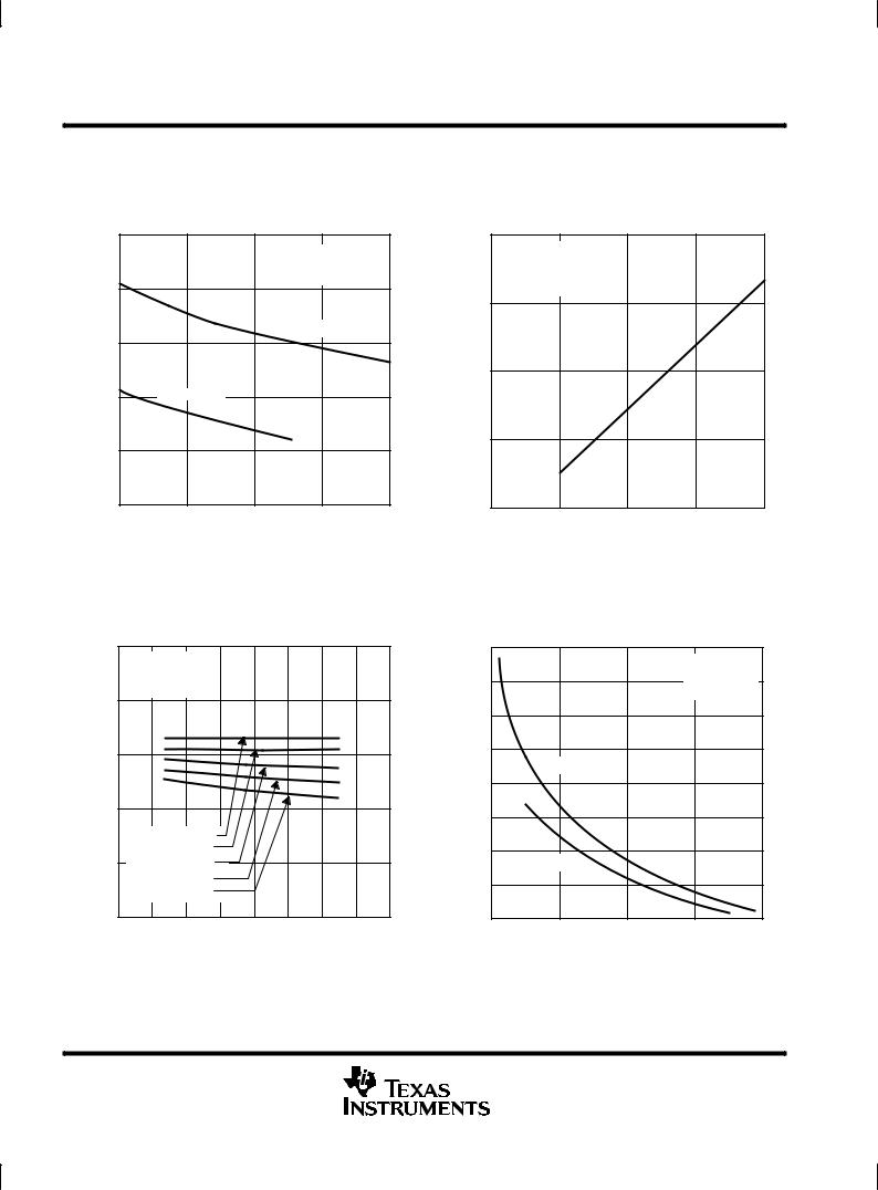
OH
VV0H ± High-Level Output Voltage ± V
5
4
3
2
1
0
0
HIGH-LEVEL OUTPUT VOLTAGE vs
HIGH-LEVEL OUTPUT CURRENT
VIC = 1 V
VID = 100 mV
TA = 25°C
VDD = 5 V
VDD = 3 V
± 2 ± 4 ± 6 ± 8
IOH ± High-Level Output Current ± mA
OH
VV0H ± High-Level Output Voltage ± V
HIGH-LEVEL OUTPUT VOLTAGE vs
SUPPLY VOLTAGE
8
VIC = 1 V VID = 100 mV RL = 1 MΩ TA = 25°C
6
4
2
0
0 |
2 |
4 |
6 |
8 |
VDD ± Supply Voltage ± V
Figure 6
HIGH-LEVEL OUTPUT VOLTAGE vs
FREE-AIR TEMPERATURE
|
3 |
VDD = 3 V |
|
|
|
|
|
|
|
|
|
|
|
|
|
|
|
|
|
VIC = 1 V |
|
|
|
|
|
|
Level-High± Output Voltage ± V |
2.4 |
VID = 100 mV |
|
|
|
|
|
Level-Low± Output Voltage ± mV |
|
|
|
|
|
|
|||
0.6 |
IOH = ± 2 mA |
|
|
|
|
|
||
|
1.8 |
|
|
|
|
|
|
|
|
1.2 |
|
|
|
|
|
|
|
|
|
IOH = ± 500 μA |
|
|
|
|
|
|
VV0H |
|
IOH = ± 1 mA |
|
|
|
|
|
VOL |
|
IOH = ± 4 mA |
|
|
|
|
|
||
OH |
|
IOH = ± 3 mA |
|
|
|
|
|
OL |
|
0 |
|
|
|
|
|
|
|
|
± 75 |
± 50 ± 25 |
0 |
25 |
50 |
75 |
100 |
125 |
|
|
TA ± Free-Air Temperature ± °C |
|
|
||||
Figure 7
LOW-LEVEL OUTPUT VOLTAGE vs
COMMON-MODE INPUT VOLTAGE
700
VDD = 5 V
650 IOL = 5 mA TA = 25°C
600
550
VID = ±100 mV
500
450
400
VID = ±1 V
350
300
0 |
1 |
2 |
3 |
4 |
|
VIC ± Common-Mode Input Voltage ± V |
|
||
Figure 8 |
Figure 9 |
12 |
POST OFFICE BOX 655303 •DALLAS, TEXAS 75265 |
TLV2341, TLV2341Y
LinCMOS PROGRAMMABLE LOW-VOLTAGE
OPERATIONAL AMPLIFIERS
SLOS110A ± MAY 1992 ± REVISED AUGUST 1994
TYPICAL CHARACTERISTICS (HIGH-BIAS MODE)
|
|
LOW-LEVEL OUTPUT VOLTAGE |
|
|||||
|
|
|
|
vs |
|
|
|
|
|
|
FREE-AIR TEMPERATURE |
|
|
||||
|
200 |
VDD = 3 V |
|
|
|
|
|
|
|
|
|
|
|
|
|
|
|
mV |
|
VIC = 1 V |
|
|
|
|
|
|
185 |
VID = ± 100 mV |
|
|
|
|
|
|
|
± |
|
IOL = 1 mA |
|
|
|
|
|
|
Voltage |
150 |
|
|
|
|
|
|
|
OutputLevel- |
125 |
|
|
|
|
|
|
|
|
|
|
|
|
|
|
|
|
± Low |
100 |
|
|
|
|
|
|
|
|
|
|
|
|
|
|
|
|
VOL |
|
|
|
|
|
|
|
|
OL |
75 |
|
|
|
|
|
|
|
|
50 |
|
|
|
|
|
|
|
|
± 75 |
± 50 ± 25 |
0 |
25 |
50 |
75 |
100 |
125 |
|
|
TA ± Free-Air Temperature ± °C |
|
|
||||
Figure 10
LOW-LEVEL OUTPUT VOLTAGE vs
FREE-AIR TEMPERATURE
|
900 |
|
|
|
|
|
|
|
|
|
|
|
|
|
|
|
|
|
|
|
|
|
|
|
|
|
|
|
|
|
|
|
|
VDD = 5 V |
|
|
|
|
|
|
|
|
||
mV |
800 |
|
|
VIC = 0.5 V |
|
|
|
|
|
|
|
|
||
|
|
|
|
|
|
|
|
|
|
|||||
|
|
|
VID = ± 1 V |
|
|
|
|
|
|
|
|
|||
± |
|
|
|
|
|
|
|
|
|
|
|
|||
700 |
|
|
IOL = 5 mA |
|
|
|
|
|
|
|
|
|||
Voltage |
|
|
|
|
|
|
|
|
|
|
||||
|
|
|
|
|
|
|
|
|
||||||
600 |
|
|
|
|
|
|
|
|
|
|
|
|
|
|
Output |
|
|
|
|
|
|
|
|
|
|
|
|
|
|
500 |
|
|
|
|
|
|
|
|
|
|
|
|
|
|
Level- |
|
|
|
|
|
|
|
|
|
|
|
|
|
|
400 |
|
|
|
|
|
|
|
|
|
|
|
|
|
|
Low± |
|
|
|
|
|
|
|
|
|
|
|
|
|
|
300 |
|
|
|
|
|
|
|
|
|
|
|
|
|
|
|
|
|
|
|
|
|
|
|
|
|
|
|
|
|
VOL |
200 |
|
|
|
|
|
|
|
|
|
|
|
|
|
|
|
|
|
|
|
|
|
|
|
|
|
|
||
|
|
|
|
|
|
|
|
|
|
|
|
|
|
|
OL |
|
|
|
|
|
|
|
|
|
|
|
|
|
|
|
100 |
|
|
|
|
|
|
|
|
|
|
|
|
|
|
|
|
|
|
|
|
|
|
|
|
|
|
|
|
|
0 |
|
|
|
|
|
|
|
|
|
|
|
|
|
|
|
|
|
|
|
|
|
|
|
|
|
|
|
|
|
± 75 |
± 50 ± 25 |
0 |
25 50 75 100 125 |
||||||||||
TA ± Free-Air Temperature ± °C
Figure 12
|
|
LOW-LEVEL OUTPUT VOLTAGE |
||||
|
|
|
|
vs |
|
|
|
|
DIFFERENTIAL INPUT VOLTAGE |
||||
|
800 |
|
|
|
VDD = 5 V |
|
|
|
|
|
|
||
mV |
700 |
|
|
|
VIC = |VID / 2| |
|
|
|
|
IOL = 5 mA |
|||
|
|
|
|
|||
± |
|
|
|
|
TA = 25°C |
|
Voltage |
600 |
|
|
|
|
|
|
|
|
|
|
|
|
Output |
500 |
|
|
|
|
|
400 |
|
|
|
|
|
|
Level |
300 |
|
|
|
|
|
± Low- |
200 |
|
|
|
|
|
VOL |
|
|
|
|
|
|
OL |
100 |
|
|
|
|
|
|
|
|
|
|
|
|
|
0 |
|
|
|
|
|
|
0 |
± 1 |
± 2 ± 3 |
± 4 ± 5 |
± 6 |
± 7 ± 8 |
|
|
|
VID ± Differential Input Voltage ± V |
|
||
Figure 11
|
|
|
|
|
LOW-LEVEL OUTPUT VOLTAGE |
|
|
||||||||||||
|
|
|
|
|
|
|
|
|
|
vs |
|
|
|
|
|
|
|
|
|
|
|
|
|
|
LOW-LEVEL OUTPUT CURRENT |
|
|
||||||||||||
|
1 |
|
|
|
|
|
|
|
|
|
|
|
|
|
|
|
|
|
|
|
|
|
VIC = 1 V |
|
|
|
|
|
|
|
|
|
|
|
|
||||
|
0.9 |
|
VID = ± 100 mV |
|
|
|
|
|
|
|
|
|
|
|
|
||||
|
|
|
|
|
|
|
|
|
|
|
|
|
|
||||||
V |
|
|
TA = 25°C |
|
|
|
|
|
|
|
|
|
|
|
|
||||
± |
0.8 |
|
|
|
|
|
|
|
|
|
|
|
|
|
|
|
|
|
|
Voltage |
|
|
|
|
|
|
|
|
|
|
|
|
|
|
|
|
|
|
|
0.7 |
|
|
|
|
|
|
|
|
|
|
|
|
VDD = 5 V |
|
|
|
|
||
|
|
|
|
|
|
|
|
|
|
|
|
|
|
|
|
|
|||
Output |
|
|
|
|
|
|
|
|
|
|
|
|
|
|
|
|
|
|
|
|
|
|
|
|
|
|
|
|
|
|
|
|
|
|
|
|
|
||
0.5 |
|
|
|
|
|
|
|
|
|
|
|
|
|
|
|
|
|
|
|
Level |
0.6 |
|
|
|
|
|
|
|
|
|
|
|
|
|
|
|
|
|
|
0.4 |
|
|
|
VDD |
|
= 3 V |
|
|
|
|
|
|
|
|
|
|
|
|
|
|
|
|
|
|
|
|
|
|
|
|
|
|
|
|
|
||||
|
|
|
|
|
|
|
|
|
|
|
|
|
|
|
|
||||
- |
|
|
|
|
|
|
|
|
|
|
|
|
|
|
|
|
|
|
|
± Low |
0.3 |
|
|
|
|
|
|
|
|
|
|
|
|
|
|
|
|
|
|
VOL |
|
|
|
|
|
|
|
|
|
|
|
|
|
|
|
|
|
|
|
OL |
0.2 |
|
|
|
|
|
|
|
|
|
|
|
|
|
|
|
|
|
|
|
|
|
|
|
|
|
|
|
|
|
|
|
|
|
|
|
|
|
|
|
0.1 |
|
|
|
|
|
|
|
|
|
|
|
|
|
|
|
|
|
|
|
|
|
|
|
|
|
|
|
|
|
|
|
|
|
|
|
|
|
|
|
0 |
|
|
|
|
|
|
|
|
|
|
|
|
|
|
|
|
|
|
|
|
|
|
|
|
|
|
|
|
|
|
|
|
|
7 |
8 |
|||
|
0 |
1 |
2 |
3 |
4 |
5 |
6 |
||||||||||||
IOL ± Low-Level Output Current ± mA
Figure 13
POST OFFICE BOX 655303 •DALLAS, TEXAS 75265 |
13 |
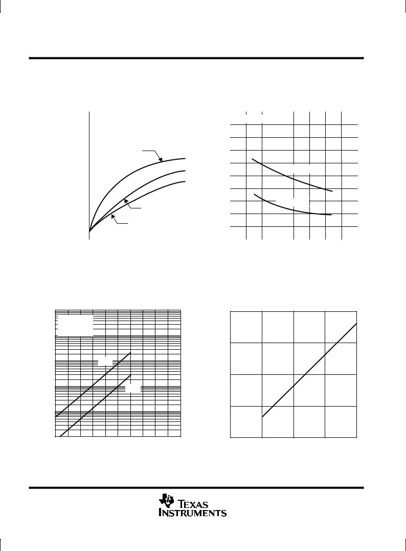
TLV2341, TLV2341Y
LinCMOS PROGRAMMABLE LOW-VOLTAGE
OPERATIONAL AMPLIFIERS
SLOS110A ± MAY 1992 ± REVISED AUGUST 1994
TYPICAL CHARACTERISTICS (HIGH-BIAS MODE)
LARGE-SIGNAL
DIFFERENTIAL VOLTAGE AMPLIFICATION vs
SUPPLY VOLTAGE
|
60 |
|
|
|
|
|
|
|
|
|
|
|
|
|
|
RL = 10 kΩ |
|
|
|
|
|
|
|
|
|
Voltage |
50 |
|
|
|
|
|
|
|
|
|
|
|
DifferentialSignal-Large V/mV±Amplification |
|
|
|
|
|
|
|
|
|
|
|
|
|
|
|
|
|
|
|
|
|
|
|
|
|
40 |
|
|
|
TA = ± 40°C |
|
|
|
|
|
|||
|
|
|
|
|
|
|
|
|
|
|
|
|
|
|
|
|
|
|
|
|
|
|
|
|
|
|
30 |
|
|
|
|
|
|
|
|
|
|
|
|
|
|
|
|
|
|
|
|
|
|
|
|
|
20 |
|
|
|
|
|
|
|
|
|
|
|
|
|
|
|
|
|
|
|
|
|
|
|
|
|
|
|
|
|
|
|
|
|
|
|
|
|
± |
|
|
|
|
|
|
TA |
= 25°C |
|
|
||
|
|
|
|
|
|
|
|
|
|
|
|
|
VD |
10 |
|
|
|
|
|
|
|
|
|
|
|
A |
|
|
|
|
|
|
TA = 85°C |
|
|
|||
|
0 |
|
|
|
|
|
|
|
|
|
|
|
|
|
2 |
4 |
6 |
8 |
|||||||
|
0 |
|||||||||||
VDD ± Supply Voltage ± V
Figure 14
INPUT BIAS CURRENT AND INPUT OFFSET
|
|
|
|
|
CURRENT |
|
|
|
|
||
|
|
|
|
|
|
vs |
|
|
|
|
|
|
104 |
|
FREE-AIR TEMPERATURE |
|
|
||||||
pA |
|
|
|
|
|
|
|
|
|
|
|
|
VDD = 3 V |
|
|
|
|
|
|
|
|
||
± |
|
|
|
|
|
|
|
|
|
||
|
VIC |
= 1 V |
|
|
|
|
|
|
|
|
|
CurrentsOffset |
102 |
|
IIB |
|
|
|
|
|
|
||
See Note A |
|
|
|
|
|
|
|
||||
|
103 |
|
|
|
|
|
|
|
|
||
|
|
|
|
|
|
|
|
|
|
|
|
Bias and |
101 |
|
|
|
|
|
IIO |
|
|
|
|
± Input |
|
|
|
|
|
|
|
|
|
|
|
IO |
1 |
|
|
|
|
|
|
|
|
|
|
andIO |
|
|
|
|
|
|
|
|
|
|
|
IB |
|
|
|
|
|
|
|
|
|
|
|
IB |
0.1 |
|
|
|
|
|
|
|
|
|
|
|
|
|
|
|
|
|
|
|
|
|
|
|
25 |
35 |
45 |
55 |
65 |
75 |
85 |
95 |
105 |
115 |
125 |
|
|
|
TA ± Free-Air Temperature ± °C |
|
|
||||||
NOTE: The typical values of input bias current and input offset current below 5 pA were determined mathematically.
Figure 16
LARGE-SIGNAL
DIFFERENTIAL VOLTAGE AMPLIFICATION vs
FREE-AIR TEMPERATURE
|
50 |
|
|
|
|
|
RL = 10 kΩ |
|
|
|
|
|
45 |
|
|
|
|
Voltage |
|
|
|
|
|
40 |
|
|
|
|
|
DifferentialSignal-Large V/mV±Amplification |
|
|
|
|
|
35 |
|
|
|
|
|
|
|
|
|
|
|
|
30 |
|
|
VDD = 5 V |
|
|
|
|
|
|
|
|
25 |
|
|
|
|
|
20 |
|
|
|
|
|
15 |
|
VDD = 3 V |
|
|
± |
10 |
|
|
|
|
VD |
|
|
|
|
|
|
|
|
|
|
|
A |
5 |
|
|
|
|
|
|
|
|
|
|
|
0 |
|
|
|
|
|
|
|
|
|
|
|
± 75 ± 50 ± 25 |
0 |
25 50 75 100 125 |
||
TA ± Free-Air Temperature ± °C
Figure 15
|
|
COMMON-MODE INPUT VOLTAGE |
|
||
|
|
|
POSITIVE LIMIT |
|
|
|
|
|
vs |
|
|
|
8 |
|
SUPPLY VOLTAGE |
|
|
|
|
|
|
|
|
± V |
|
TA = 25°C |
|
|
|
|
|
|
|
|
|
Input Voltage |
6 |
|
|
|
|
Mode-Common |
4 |
|
|
|
|
|
|
|
|
|
|
± |
2 |
|
|
|
|
|
|
|
|
|
|
IC |
|
|
|
|
|
VIC |
|
|
|
|
|
|
0 |
|
|
|
|
|
0 |
2 |
4 |
6 |
8 |
|
|
VDD ± Supply Voltage ± V |
|
||
Figure 17
14 |
POST OFFICE BOX 655303 •DALLAS, TEXAS 75265 |
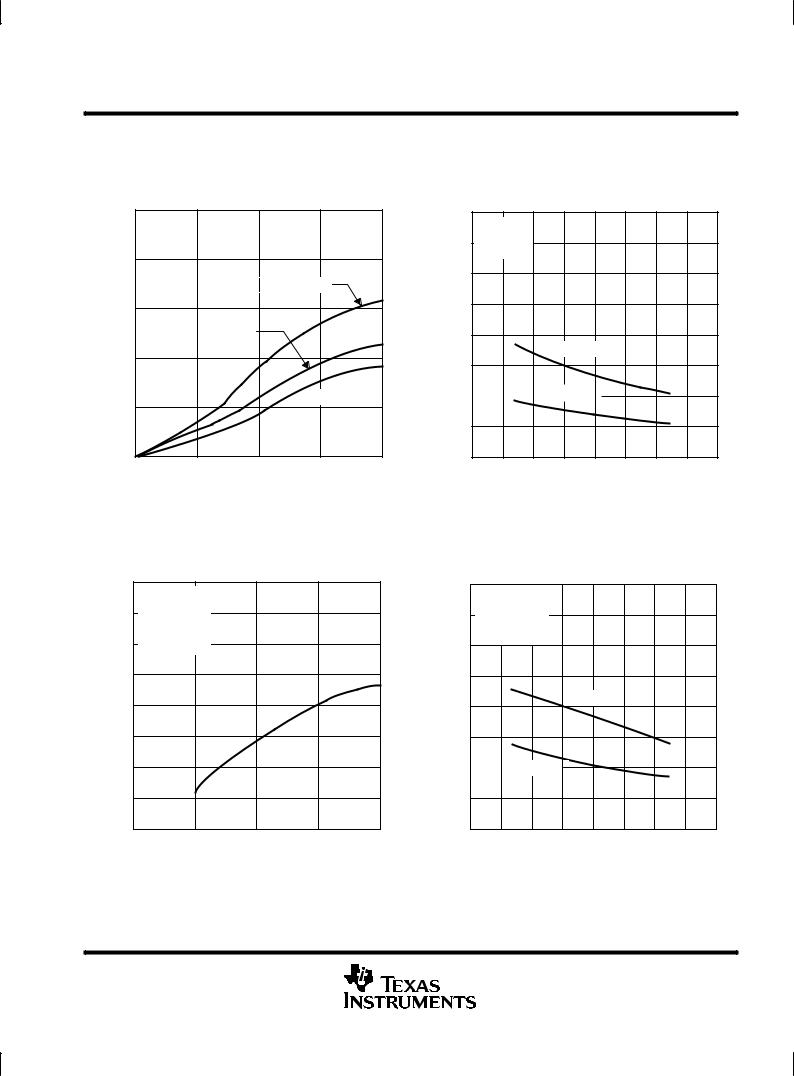
TLV2341, TLV2341Y
LinCMOS PROGRAMMABLE LOW-VOLTAGE
OPERATIONAL AMPLIFIERS
SLOS110A ± MAY 1992 ± REVISED AUGUST 1994
TYPICAL CHARACTERISTICS (HIGH-BIAS MODE)
|
|
SUPPLY CURRENT |
|
|
|
|
vs |
|
|
|
|
SUPPLY VOLTAGE |
|
|
2 |
VIC = 1 V |
|
|
|
|
|
|
|
|
|
VO = 1 V |
|
|
|
1.6 |
No Load |
|
|
|
|
|
|
|
|
CurrentSupply± ± mA |
|
TA = ± 40°C |
CurrentSupply± ± mA |
|
|
|
|
||
1.2 |
|
|
|
|
|
|
TA = 25°C |
|
|
0.8 |
|
|
|
IIDD |
IIDD |
|
|
|
|
DD |
|
|
TA = 85°C |
DD |
0.4 |
|
|
|
|
|
|
|
|
|
0 |
|
|
|
|
0 |
2 |
4 |
6 |
8 |
|
VDD ± Supply Voltage ± V |
|
||
Figure 18
SUPPLY CURRENT vs
FREE-AIR TEMPERATURE
2
VIC = 1 V
1.75VO = 1 V No Load
1.5
1.25
1
VDD = 5 V
0.75
0.5 |
|
VDD = 3 V |
|
0.25
0 |
|
|
|
|
±75 ± 50 ± 25 |
0 |
25 |
50 |
75 100 125 |
TA ± Free-Air Temperature ± °C
Figure 19
SR ± Slew Rate ± usV/μ
SLEW RATE vs
SUPPLY VOLTAGE
8 VI(PP) = 1 V AV = 1
7RL = 10 kΩ
CL = 20 pF
6 TA = 25°C
5
4
3
2
1
0
0 |
2 |
4 |
6 |
8 |
VDD ± Supply Voltage ± V
Figure 20
SR ± Slew Rate ± usV/μ
SLEW RATE vs
FREE-AIR TEMPERATURE
8 
 VI(PP) = 1 V AV = 1
7RL = 10 kΩ
CL = 20 pF
6
5
VDD = 5 V
4
3
2  VDD = 3 V
1
0
± 75 ± 50 ± 25 0 25 50 75 100 125 TA ± Free-Air Temperature ± °C
Figure 21
POST OFFICE BOX 655303 •DALLAS, TEXAS 75265 |
15 |

TLV2341, TLV2341Y
LinCMOS PROGRAMMABLE LOW-VOLTAGE
OPERATIONAL AMPLIFIERS
SLOS110A ± MAY 1992 ± REVISED AUGUST 1994
TYPICAL CHARACTERISTICS (HIGH-BIAS MODE)
Bias Select Current ± μnA
BIAS SELECT CURRENT |
MAXIMUM PEAK-TO-PEAK OUTPUT VOLTAGE |
|
|
vs |
|
|
|
|
|
vs |
|
|
|
|
SUPPLY VOLTAGE |
|
|
|
|
FREQUENCY |
|
|
|
± 3 |
|
|
|
|
V |
5 |
|
|
|
|
|
° |
|
|
|
± |
|
|
R |
L |
= 10 kΩ |
|
|
|
|
|
|
|
||||
|
TA = 25 C |
|
|
|
Voltage |
|
|
|
|
|
|
VI(SEL) = 0 |
|
|
|
VDD = 5 V |
|
|
|
||
|
|
|
|
|
|
|
|
|||
± 2.4 |
|
|
|
|
|
|
|
|
||
|
|
|
|
Output |
4 |
|
|
|
|
|
|
|
|
|
|
VDD = 3 V |
|
|
|
||
± 1.8 |
|
|
|
|
Peak-to- |
|
|
|
||
|
|
|
|
|
3 |
|
|
|
|
|
± 1.2 |
|
|
|
|
Peak |
2 |
|
|
TA = ± 40°C |
|
|
|
|
|
|
|
|
||||
|
|
|
|
|
Maximum± |
|
|
|
||
|
|
|
|
|
TA |
= 85°C |
|
|
|
|
|
|
|
|
|
|
TA = 25°C |
|
|
|
|
± 0.6 |
|
|
|
|
|
1 |
|
|
|
|
|
|
|
|
|
O(PP) |
0 |
|
|
|
|
0 |
2 |
4 |
6 |
8 |
V |
|
|
|
|
|
10 |
10 0 |
1000 |
|
10000 |
||||||
|
|
|||||||||
|
VDD ± Supply Voltage ± V |
|
|
|
f ± Frequency ± kHz |
|
|
|||
1 ± Unity-Gain Bandwidth ± MHz B1
Figure 22 |
Figure 23 |
|
|
UNITY-GAIN BANDWIDTH |
|
|
|
|
UNITY-GAIN BANDWIDTH |
|
|
||||||||
|
|
|
|
vs |
|
|
|
|
|
|
|
|
vs |
|
|
|
|
|
|
FREE-AIR TEMPERATURE |
|
|
|
|
|
SUPPLY VOLTAGE |
|
|
|
||||||
3.5 |
|
|
|
|
|
|
|
|
2.1 |
|
|
|
|
|
|
|
|
VI = 10 mV |
|
|
|
|
|
|
|
VI = 10 mV |
|
|
|
|
|
|
|||
RL = 10 kΩ |
|
|
|
|
|
|
1.9 |
RL = 10 kΩ |
|
|
|
|
|
|
|||
CL = 20 pF |
|
|
|
|
|
MHz± |
1.7 |
CL = 20 pF |
|
|
|
|
|
|
|||
2.9 |
|
|
|
|
|
|
|
TA = 25°C |
|
|
|
|
|
|
|||
|
|
|
|
|
|
|
|
|
|
|
|
|
|
||||
|
|
|
|
|
|
|
|
Bandwidth |
1.5 |
|
|
|
|
|
|
|
|
2.3 |
|
|
|
|
|
|
|
1.1 |
|
|
|
|
|
|
|
|
|
|
|
|
|
|
|
|
|
1.3 |
|
|
|
|
|
|
|
|
|
|
|
|
|
VDD = 5 V |
|
|
Gain |
|
|
|
|
|
|
|
|
|
|
1.7 |
|
|
|
|
|
|
|
0.9 |
|
|
|
|
|
|
|
|
|
|
|
|
|
|
|
|
|
- |
|
|
|
|
|
|
|
|
|
|
|
|
|
|
|
|
|
Unity± |
0.7 |
|
|
|
|
|
|
|
|
|
|
|
|
|
|
|
|
|
|
|
|
|
|
|
|
|
|
1.1 |
|
|
|
|
|
|
|
1 |
0.5 |
|
|
|
|
|
|
|
|
|
|
|
|
VDD = 3 V |
|
|
1B |
|
|
|
|
|
|
|
|
|
|
|
|
|
|
|
|
|
0.3 |
|
|
|
|
|
|
|
|
||
|
|
|
|
|
|
|
|
|
|
|
|
|
|
|
|
|
|
0.5 |
|
|
|
|
|
|
|
|
0.1 |
|
|
|
|
|
|
|
|
± 75 |
± 50 |
± 25 |
0 |
25 |
50 |
75 |
100 |
125 |
0 |
1 |
2 |
3 |
4 |
5 |
6 |
7 |
8 |
|
|
TA ± Free-Air Temperature ± °C |
|
|
|
|
VDD ± Supply Voltage ± V |
|
|
||||||||
Figure 24 |
Figure 25 |
16 |
POST OFFICE BOX 655303 •DALLAS, TEXAS 75265 |
 Loading...