


Texas Instruments TLV2324IPWR, TLV2324IPWLE, TLV2324IPW, TLV2324IN, TLV2324IDR Datasheet
...TLV2322, TLV2322Y, TLV2324, TLV2324Y LinCMOS LOW-VOLTAGE LOW-POWER
OPERATIONAL AMPLIFIERS
SLOS187 ± FEBRUARY 1997
DWide Range of Supply Voltages Over Specified Temperature Range:
TA = ±40°C to 85°C . . . 2 V to 8 V
DFully Characterized at 3 V and 5 V
DSingle-Supply Operation
DCommon-Mode Input Voltage Range
Extends Below the Negative Rail and up to VDD ±1 V at TA = 25°C
TLV2322
D OR P PACKAGE
(TOP VIEW)
1OUT |
|
1 |
8 |
|
VDD |
|
|
||||
1IN ± |
|
|
|
|
|
|
2 |
7 |
|
2OUT |
|
1IN + |
|
3 |
6 |
|
2IN ± |
|
|
||||
VDD ±/GND |
|
4 |
5 |
|
2IN + |
|
|
||||
|
|
|
|
|
|
|
|
|
|
|
|
DOutput Voltage Range Includes Negative Rail
DHigh Input Impedance . . . 1012 Ω Typical
DESD-Protection Circuitry
DDesigned-In Latch-Up Immunity
description
The TLV232x operational amplifiers are in a family of devices that has been specifically designed for use in low-voltage single-supply applications. This amplifier is especially well suited to ultra-low-power systems that require devices to consume the absolute minimum of supply currents. Each amplifier is fully functional down to a minimum supply voltage of 2 V, is fully characterized, tested, and specified at both 3-V and 5-V power supplies. The common-mode input voltage range includes the negative rail and extends to within 1 V of the positive rail.
These amplifiers are specifically targeted for use in very low-power, portable, battery-driven applications with the maximum supply current per operational amplifier specified at only 27 μA over its full temperature range of ±40°C to 85°C.
TLV2322
PW PACKAGE (TOP VIEW)
1OUT |
1 |
8 |
|
|
VDD + |
|
|
||||
|
|
||||
1IN± |
2 |
7 |
|
|
2OUT |
1IN + |
3 |
6 |
|
|
2IN ± |
|
|
||||
VDD ±/ GND |
4 |
5 |
|
|
2IN + |
|
|
||||
|
|
TLV2324
D OR N PACKAGE
(TOP VIEW)
1OUT |
|
1 |
14 |
|
4OUT |
|||
|
|
|||||||
1IN ± |
|
2 |
13 |
|
4IN ± |
|||
|
|
|||||||
1IN + |
|
3 |
12 |
|
4IN + |
|||
|
|
|||||||
VDD+ |
|
4 |
11 |
|
VDD ±/ GND |
|||
|
|
|||||||
|
|
|||||||
2IN + |
|
5 |
10 |
|
3IN + |
|||
2IN ± |
|
6 |
9 |
|
3IN ± |
|||
|
|
|||||||
2OUT |
|
7 |
8 |
|
3OUT |
|||
|
|
|||||||
|
|
|
|
|
|
|
|
|
|
|
|
TLV2324 |
|
|
|
||
|
PW PACKAGE |
|
|
|
||||
|
|
(TOP VIEW) |
|
|
|
|||
|
|
|
|
|
|
|
||
1OUT |
|
1 |
14 |
|
|
|
4OUT |
|
|
|
|
||||||
1IN ± |
|
|
|
|
|
|
|
4IN ± |
|
|
|
|
|
|
|||
1IN + |
|
|
|
|
|
|
|
4IN + |
|
|
|
|
|
|
|||
VDD+ |
|
|
|
|
|
|
|
VDD ±/ GND |
|
|
|
|
|
|
|||
2IN + |
|
|
|
|
|
|
|
3IN + |
2IN ± |
|
|
|
|
|
|
|
3IN ± |
2OUT |
|
7 |
8 |
|
|
|
3OUT |
|
|
|
|
|
|
|
|
|
|
AVAILABLE OPTIONS
|
V max AT |
|
PACKAGED DEVICES |
|
CHIP FORM§ |
||
|
|
|
|
|
|||
|
|
|
|
|
|||
TA |
IO |
SMALL OUTLINE² |
PLASTIC DIP |
PLASTIC DIP |
TSSOP³ |
|
|
25°C |
(Y) |
||||||
|
(D) |
(N) |
(P) |
(PW) |
|||
|
|
|
|||||
±40°C to 85°C |
9 mV |
TLV2322ID |
Ð |
TLV2322IP |
TLV2322IPWLE |
TLV2322Y |
|
|
|
|
|
|
|
||
10 mV |
TLV2324ID |
TLV2324IN |
Ð |
TLV2324IPWLE |
TLV2324Y |
||
|
|||||||
² The D package is available taped and reeled. Add R suffix to the device type (e.g., TLV2322IDR). ³ The PW package is only available left-end taped and reeled (e.g., TLV2322IPWLE).
§ Chip forms are tested at 25°C only.
Please be aware that an important notice concerning availability, standard warranty, and use in critical applications of Texas Instruments semiconductor products and disclaimers thereto appears at the end of this data sheet.
LinCMOS is a trademark of Texas Instruments Incorporated.
PRODUCTION DATA information is current as of publication date. Products conform to specifications per the terms of Texas Instruments standard warranty. Production processing does not necessarily include testing of all parameters.
Copyright 1997, Texas Instruments Incorporated
POST OFFICE BOX 655303 •DALLAS, TEXAS 75265 |
1 |

TLV2322, TLV2322Y, TLV2324, TLV2324Y
LinCMOS LOW-VOLTAGE LOW-POWER
OPERATIONAL AMPLIFIERS
SLOS187 ± FEBRUARY 1997
description (continued)
Low-voltage and low-power operation has been made possible by using the Texas Instruments silicon-gate LinCMOS technology. The LinCMOS process also features extremely high input impedance and ultra-low bias currents making these amplifiers ideal for interfacing to high-impedance sources such as sensor circuits or filter applications.
To facilitate the design of small portable equipment, the TLV232x is made available in a wide range of package options, including the small-outline and thin-shrink small-outline packages (TSSOP). The TSSOP package has significantly reduced dimensions compared to a standard surface-mount package. Its maximum height of only 1.1 mm makes it particularly attractive when space is critical.
The device inputs and outputs are designed to withstand ±100-mA currents without sustaining latch-up. The TLV232x incorporates internal ESD-protection circuits that prevent functional failures at voltages up to 2000 V as tested under MIL-STD 883C, Method 3015.2; however, care should be exercised in handling these devices as exposure to ESD can result in the degradation of the device parametric performance.
TLV2322Y chip information
This chip, when properly assembled, displays characteristics similar to the TLV2322I. Thermal compression or ultrasonic bonding may be used on the doped-aluminum bonding pads. Chips may be mounted with conductive epoxy or a gold-silicon preform.
BONDING PAD ASSIGNMENTS
|
|
|
|
(5) |
(4) |
(3) |
||
|
|
(6) |
|
|
(2) |
|||
|
|
|
|
|
|
|
||
59 |
|
|
|
|
|
|||
|
|
(7) |
|
|
(1) |
|||
|
|
|
|
|
|
(8) |
|
|
|
|
|
|
|
|
|
|
|
|
|
|
|
|
|
|
|
|
|
|
|
|
|
|
72 |
|
|
|
|
VDD |
||||
|
(3) |
|
(8) |
|
|
|
1IN + |
+ |
|
|
|
||
|
|
|
1OUT |
|||
(2) |
||||||
|
|
|||||
1IN ± |
± |
|
|
|||
|
|
|||||
|
|
|
||||
|
|
|
|
|||
(5) |
||||||
2IN + |
+ |
|
|
|
||
|
|
|
2OUT |
|||
(6) |
|
|
||||
2IN ± |
± |
|
|
|||
|
|
|||||
|
|
|
||||
|
|
|
|
|||
|
|
|
|
|||
(4) VDD ± /GND
CHIP THICKNESS: 15 MILS TYPICAL BONDING PADS: 4 × 4 MILS MINIMUM TJmax = 150°C
TOLERANCES ARE ± 10%.
ALL DIMENSIONS ARE IN MILS.
2 |
POST OFFICE BOX 655303 •DALLAS, TEXAS 75265 |
TLV2322, TLV2322Y, TLV2324, TLV2324Y
LinCMOS LOW-VOLTAGE LOW-POWER
OPERATIONAL AMPLIFIERS
SLOS187 ± FEBRUARY 1997
TLV2324Y chip information
This chip, when properly assembled, display characteristics similar to the TLV2324. Thermal compression or ultrasonic bonding may be used on the doped-aluminum bonding pads. Chips may be mounted with conductive epoxy or a gold-silicon preform.
|
|
|
|
|
|
|
|
|
|
|
|
|
|
|
|
|
|
|
|
|
|
|
|
|
|
|
|
BONDING PAD ASSIGNMENTS |
|
|
|
|
|
|
|
|
|
|
|
|
|
|
|
|
|
|
|
|
|
|
|
|
|
|
|
|
|
|
|
|
|
|
|
|
|
|
|
|
|
|
|
|
|
||||||||||||||||||||||||||||||||||||||||
|
|
|
|
|
|
|
|
|
|
|
|
|
|
|
|
|
|
|
|
|
|
|
|
|
|
|
|
|
|
|
|
|
|
|
|
|
|
|
|
|
|
|
|
|
|
|
|
|
|
|
|
|
|
|
|
|
|
|
|
|
|
|
|
|
|
|
|
|
|
|
|
|
|
|
|
|
|
|
|
|
|
|
|
|
|
|
|
|
|
|
|
|
|
|
|
|
|
|
|
|
|
|
|
|
|
|
|
VDD |
|
|
|
||
|
|
|
|
|
|
|
|
|
(14) |
(13) |
(12) (11) |
|
|
|
(10) |
|
(9) |
|
|
|
|
|
|
|
|
|
(8) |
|
|
|
|
|
1IN + |
(3) |
|
|
+ |
(4) |
|
(1) |
|
1OUT |
|||||||||||||||||||||||||||||||||||||||||||||||||||||||||||||||||||||||
|
|
|
|
|
|
|
|
|
|
|
|
|
|
|
|
|
|
|
|
|
|
|
|
|
|
|
|
|
|
|
|||||||||||||||||||||||||||||||||||||||||||||||||||||||||||||||||||||||||||||||||||
|
|
|
|
|
|
|
|
|
|
|
|
|
|
|
|
|
|
|
|
|
|
|
|
|
|
|
|
|
|
|
|
||||||||||||||||||||||||||||||||||||||||||||||||||||||||||||||||||||||||||||||||||
|
|
|
|
|
|
|
|
|
|
|
|
|
|
|
|
|
|
|
|
|
|
|
|
|
|
|
|
|
|
|
|
||||||||||||||||||||||||||||||||||||||||||||||||||||||||||||||||||||||||||||||||||
|
|
|
|
|
|
|
|
|
|
|
|
|
|
|
|
|
|
|
|
|
|
|
|
|
|
|
|
|
|
||||||||||||||||||||||||||||||||||||||||||||||||||||||||||||||||||||||||||||||||||||
|
|
|
|
|
|
|
|
|
|
|
|
|
|
|
|
|
|
|
|
|
|
|
|
|
|
|
|
|
|
|
|
|
|
|
|
|
|
|
|
|
|
|
|
|
|
|
|
|
|
|
|
|
|
|
|
|
|
|
|
|
|
|
|
|
|
|
|
|
|
|
|
|
|
|
|
|
|
|
|
|
|
|
|
|
|
|
|
|
|
|
|
|
|
|
|
|
|
|
|
|
|
|
1IN ± |
(2) |
|
|
± |
|
|
|
|||
|
|
|
|
|
|
|
|
|
|
|
|
|
|
|
|
|
|
|
|
|
|
|
|
|
|
|
|
|
|
|
|
|
|
|
|
|
|
|
|
|
|
|
|
|
|
|
|
|
|
|
|
|
|
|
|
|
|
|
|
|
|
|
|
|
|
|
|
|
|
|
|
|
|
|
|
|
|
|
|
|
|
|
|
|
|
|
|
|
|
|
|
|
|
|
|
|
|
|
|
|
|
|
|
|
|
|
|
||||||
|
|
|
|
|
|
|
|
|
|
|
|
|
|
|
|
|
|
|
|
|
|
|
|
|
|
|
|
|
|
|
|
|
|
|
|
|
|
|
|
|
|
|
|
|
|
|
|
|
|
|
|
|
|
|
|
|
|
|
|
|
|
|
|
|
|
|
|
|
|
|
|
|
|
|
|
|
|
|
|
|
|
|
|
|
|
|
|
|
|
|
|
|
|
|
|
|
|
|
|
|
|
|
|
|
|
|
|
|
|||||
|
|
|
|
|
|
|
|
|
|
|
|
|
|
|
|
|
|
|
|
|
|
|
|
|
|
|
|
|
|
|
|
|
|
|
|
|
|
|
|
|
|
|
|
|
|
|
|
|
|
|
|
|
|
|
|
|
|
|
|
|
|
|
|
|
|
|
|
|
|
|
|
|
|
|
|
|
|
|
|
|
|
|
|
|
|
|
|
|
|
|
|
|
|
|
|
|
|
|
|
|
|
|
|
|
|
|
|
|
|||||
|
|
|
|
|
|
|
|
|
|
|
|
|
|
|
|
|
|
|
|
|
|
|
|
|
|
|
|
|
|
|
|
|
|
|
|
|
|
|
|
|
|
|
|
|
|
|
|
|
|
|
|
|
|
|
|
|
|
|
|
|
|
|
|
|
|
|
|
|
|
|
|
|
|
|
|
|
|
|
|
|
|
|
|
|
|
|
|
|
|
|
|
|
|
|
|
|
|
|
|
|
|
|
|
|
|
|
|
|
|
||||
|
|
|
|
|
|
|
|
|
|
|
|
|
|
|
|
|
|
|
|
|
|
|
|
|
|
|
|
|
|
|
|
|
|
|
|
|
|
|
|
|
|
|
|
|
|
|
|
|
|
|
|
|
|
|
|
|
|
|
|
|
|
|
|
|
|
|
|
|
|
|
|
|
|
|
|
|
|
|
|
|
|
|
|
|
|
|
|
|
|
|
|
|
|
|
|
|
|
|
|
|
|
|
|
|
|
|
|
|
|
|
|||
|
|
|
|
|
|
|
|
|
|
|
|
|
|
|
|
|
|
|
|
|
|
|
|
|
|
|
|
|
|
|
|
|
|
|
|
|
|
|
|
|
|
|
|
|
|
|
|
|
|
|
|
|
|
|
|
|
|
|
|
|
|
|
|
|
|
|
|
|
|
|
|
|
|
|
|
|
|
|
|
|
|
|
|
|
|
|
|
|
|
|
|
|
|
|
|
|
|
|
|
|
|
|
(5) |
|
|
|
|
|
|
|
|||
|
|
|
|
|
|
|
|
|
|
|
|
|
|
|
|
|
|
|
|
|
|
|
|
|
|
|
|
|
|
|
|
|
|
|
|
|
|
|
|
|
|
|
|
|
|
|
|
|
|
|
|
|
|
|
|
|
|
|
|
|
|
|
|
|
|
|
|
|
|
|
|
|
|
|
|
|
|
|
|
|
|
|
|
|
|
|
|
|
|
|
|
|
|
|
|
|
|
|
|
|
|
|
|
|
|
|
|
|
|
||||
|
|
|
|
|
|
|
|
|
|
|
|
|
|
|
|
|
|
|
|
|
|
|
|
|
|
|
|
|
|
|
|
|
|
|
|
|
|
|
|
|
|
|
|
|
|
|
|
|
|
|
|
|
|
|
|
|
|
|
|
|
|
|
|
|
|
|
|
|
|
|
|
|
|
|
|
|
|
|
|
|
|
|
|
|
|
|
|
|
|
|
|
|
|
|
|
|
|
|
|
|
|
|
2IN + |
|
|
+ |
|
|
(7) |
|
2OUT |
||
|
|
|
|
|
|
|
|
|
|
|
|
|
|
|
|
|
|
|
|
|
|
|
|
|
|
|
|
|
|
|
|
|
|
|
|
|
|
|
|
|
|
|
|
|
|
|
|
|
|
|
|
|
|
|
|
|
|
|
|
|
|
|
|
|
|
|
|
|
|
|
|
|
|
|
|
|
|
|
|
|
|
|
|
|
|
|
|
|
|
|
|
|
|
|
|
|
|
|
|
|
|
|
|
|
|
|
|
||||||
|
|
|
|
|
|
|
|
|
|
|
|
|
|
|
|
|
|
|
|
|
|
|
|
|
|
|
|
|
|
|
|
|
|
|
|
|
|
|
|
|
|
|
|
|
|
|
|
|
|
|
|
|
|
|
|
|
|
|
|
|
|
|
|
|
|
|
|
|
|
|
|
|
|
|
|
|
|
|
|
|
|
|
|
|
|
|
|
|
|
|
|
|
|
|
|
|
|
|
|
|
|
|
|
|
|
|
|
||||||
|
|
|
|
|
|
|
|
|
|
|
|
|
|
|
|
|
|
|
|
|
|
|
|
|
|
|
|
|
|
|
|
|
|
|
|
|
|
|
|
|
|
|
|
|
|
|
|
|
|
|
|
|
|
|
|
|
|
|
|
|
|
|
|
|
|
|
|
|
|
|
|
|
|
|
|
|
|
|
|
|
|
|
|
|
|
|
|
|
|
|
|
|
|
|
|
|
|
|
|
|
|
|
|
|
|
|
|
||||||
|
|
|
|
|
|
|
|
|
|
|
|
|
|
|
|
|
|
|
|
|
|
|
|
|
|
|
|
|
|
|
|
|
|
|
|
|
|
|
|
|
|
|
|
|
|
|
|
|
|
|
|
|
|
|
|
|
|
|
|
|
|
|
|
|
|
|
|
|
|
|
|
|
|
|
|
|
|
|
|
|
|
|
|
|
|
|
|
|
|
|
|
|
|
|
|
|
|
|
|
|
|
|
|
|
|
|
|
||||||
|
|
|
|
|
|
|
|
|
|
|
|
|
|
|
|
|
|
|
|
|
|
|
|
|
|
|
|
|
|
|
|
|
|
|
|
|
|
|
|
|
|
|
|
|
|
|
|
|
|
|
|
|
|
|
|
|
|
|
|
|
|
|
|
|
|
|
|
|
|
|
|
|
|
|
|
|
|
|
|
|
|
|
|
|
|
|
|
|
|
|
|
|
|
|
|
|
|
|
|
|
|
|
|
|
|
|
|
||||||
|
|
|
|
|
|
|
|
|
|
|
|
|
|
|
|
|
|
|
|
|
|
|
|
|
|
|
|
|
|
|
|
|
|
|
|
|
|
|
|
|
|
|
|
|
|
|
|
|
|
|
|
|
|
|
|
|
|
|
|
|
|
|
|
|
|
|
|
|
|
|
|
|
|
|
|
|
|
|
|
|
|
|
|
|
|
|
|
|
|
|
|
|
|
|
|
|
|
|
|
|
|
|
(6) |
|
|
|
|
|
|||||
|
|
|
|
|
|
|
|
|
|
|
|
|
|
|
|
|
|
|
|
|
|
|
|
|
|
|
|
|
|
|
|
|
|
|
|
|
|
|
|
|
|
|
|
|
|
|
|
|
|
|
|
|
|
|
|
|
|
|
|
|
|
|
|
|
|
|
|
|
|
|
|
|
|
|
|
|
|
|
|
|
|
|
|
|
|
|
|
|
|
|
|
|
|
|
|
|
|
|
|
|
|
|
2IN ± |
|
|
± |
|
|
|
||||
|
|
|
|
|
|
|
|
|
|
|
|
|
|
|
|
|
|
|
|
|
|
|
|
|
|
|
|
|
|
|
|
|
|
|
|
|
|
|
|
|
|
|
|
|
|
|
|
|
|
|
|
|
|
|
|
|
|
|
|
|
|
|
|
|
|
|
|
|
|
|
|
|
|
|
|
|
|
|
|
|
|
|
|
|
|
|
|
|
|
|
|
|
|
|
|
|
|
|
|
|
|
|
|
|
|
|
|
|
|||||
|
|
|
|
|
|
|
|
|
|
|
|
|
|
|
|
|
|
|
|
|
|
|
|
|
|
|
|
|
|
|
|
|
|
|
|
|
|
|
|
|
|
|
|
|
|
|
|
|
|
|
|
|
|
|
|
|
|
|
|
|
|
|
|
|
|
|
|
|
|
|
|
|
|
|
|
|
|
|
|
|
|
|
|
|
|
|
|
|
|
|
|
|
|
|
|
|
|
|
|
|
|
|
|
|
|
|
|
|
|||||
|
|
|
|
|
|
|
|
|
|
|
|
|
|
|
|
|
|
|
|
|
|
|
|
|
|
|
|
|
|
|
|
|
|
|
|
|
|
|
|
|
|
|
|
|
|
|
|
|
|
|
|
|
|
|
|
|
|
|
|
|
|
|
|
|
|
|
|
|
|
|
|
|
|
|
|
|
|
|
|
|
|
|
|
|
|
|
|
|
|
|
|
|
|
|
|
|
|
|
|
|
|
|
|
|
|
|
|
|
|
||||
|
|
|
|
|
|
|
|
|
|
|
|
|
|
|
|
|
|
|
|
|
|
|
|
|
|
|
|
|
|
|
|
|
|
|
|
|
|
|
|
|
|
|
|
|
|
|
|
|
|
|
|
|
|
|
|
|
|
|
|
|
|
|
|
|
|
|
|
|
|
|
|
|
|
|
|
|
|
|
|
|
|
|
|
|
|
|
|
|
|
|
|
|
|
|
|
|
|
|
|
|
|
|
|
|
|
|
|
|
|
|
|||
|
|
|
|
|
|
|
|
|
|
|
|
|
|
|
|
|
|
|
|
|
|
|
|
|
|
|
|
|
|
|
|
|
|
|
|
|
|
|
|
|
|
|
|
|
|
|
|
|
|
|
|
|
|
|
|
|
|
|
|
|
|
|
|
|
|
|
|
|
|
|
|
|
|
|
|
|
|
|
|
|
|
|
|
|
|
|
|
|
|
|
|
|
|
|
|
|
|
|
|
|
|
|
|
|
|
|
|
|
|
||||
|
|
|
|
68 |
|
|
|
|
|
|
|
|
|
|
|
|
|
|
|
|
|
|
|
|
|
|
|
|
|
|
|
|
|
|
|
|
|
|
|
|
|
|
|
|
|
|
|
|
|
|
|
|
|
|
|
|
|
|
|
|
|
|
|
|
|
|
|
|
|
|
|
|
|
|
|
|
|
|
|
|
|
|
|
|
|
|
|
|
|
|
|
|
|
|
|
|
|
|
|
3IN + |
(10) |
|
|
+ |
|
|
(8) |
|
3OUT |
||||
|
|
|
|
|
|
|
|
|
|
|
|
|
|
|
|
|
|
|
|
|
|
|
|
|
|
|
|
|
|
|
|
|
|
|
|
|
|
|
|
|
|
|
|
|
|
|
|
|
|
|
|
|
|
|
|
|
|
|
|
|
|
|
|
|
|
|
|
|
|
|
|
|
|
|
|
|
|
|
|
|
|
|
|
|
|
|
|
|
|
|
|
|
|
|
|
|
|
|
|
|
|
|
|
||||||||||
|
|
|
|
|
|
|
|
|
|
|
|
|
|
|
|
|
|
|
|
|
|
|
|
|
|
|
|
|
|
|
|
|
|
|
|
|
|
|
|
|
|
|
|
|
|
|
|
|
|
|
|
|
|
|
|
|
|
|
|
|
|
|
|
|
|
|
|
|
|
|
|
|
|
|
|
|
|
|
|
|
|
|
|
|
|
|
|
|
|
|
|
|
|
|
|
|
|
|
|
|
|
|
|
|
|
|
|
||||||
|
|
|
|
|
|
|
|
|
|
|
|
|
|
|
|
|
|
|
|
|
|
|
|
|
|
|
|
|
|
|
|
|
|
|
|
|
|
|
|
|
|
|
|
|
|
|
|
|
|
|
|
|
|
|
|
|
|
|
|
|
|
|
|
|
|
|
|
|
|
|
|
|
|
|
|
|
|
|
|
|
|
|
|
|
|
|
|
|
|
|
|
|
|
|
|
|
|
|
|
|
|
|
3IN ± |
(9) |
|
|
± |
|
|
|
|
|
|
|
|
|
|
|
|
|
|
|
|
|
|
|
|
|
|
|
|
|
|
|
|
|
|
|
|
|
|
|
|
|
|
|
|
|
|
|
|
|
|
|
|
|
|
|
|
|
|
|
|
|
|
|
|
|
|
|
|
|
|
|
|
|
|
|
|
|
|
|
|
|
|
|
|
|
|
|
|
|
|
|
|
|
|
|
|
|
|
|
|
|
|
|
|
|
|
|
|
|
|
|
|
|
|
|
|
|
|
|
|
||||
|
|
|
|
|
|
|
|
|
|
|
|
|
|
|
|
|
|
|
|
|
|
|
|
|
|
|
|
|
|
|
|
|
|
|
|
|
|
|
|
|
|
|
|
|
|
|
|
|
|
|
|
|
|
|
|
|
|
|
|
|
|
|
|
|
|
|
|
|
|
|
|
|
|
|
|
|
|
|
|
|
|
|
|
|
|
|
|
|
|
|
|
|
|
|
|
|
|
|
|
|
|
|
(12) |
|
|
|
|
|
|
|
|||
|
|
|
|
|
|
|
|
|
|
|
|
|
|
|
|
|
|
|
|
|
(2) |
|
|
|
|
|
|
|
|
|
|
|
|
|
|
|
|
|
|
|
|
|
|
|
|
|
|
|
|
|
|
(6) |
|
|
|
|
|
|
|
|
|
|
|
|
|
|
|
|
|
|
|
|
|
|
|
4IN + |
|
|
+ |
|
|
(14) |
4OUT |
||||||||||||||||||||||||||||||
|
|
|
|
|
|
|
|
|
|
|
|
|
|
|
|
|
|
|
|
|
|
|
|
|
|
|
|
|
|
|
|
|
|
|
|
|
|
|
|
|
|
|
|
|
|
|
|
|
|
|
|
|
|
|
|
|
|
|
|
|
|
|
|
|
|
|
|
|
|
|
|
|
|
|
|
|
|
||||||||||||||||||||||||||||||||||||
|
|
|
|
|
|
|
|
|
|
|
|
|
|
|
|
|
|
|
|
|
|
|
|
|
|
|
|
|
|
|
|
|
|
|
|
|
|
|
|
|
|
|
|
|
|
|
|
|
|
|
|
|
|
|
|
|
|
|
|
|
|
|
|
|
|
|
|
|
|
|
|
|
|
|
|
|
|
||||||||||||||||||||||||||||||||||||
|
|
|
|
|
|
|
|
|
|
|
|
|
|
|
|
|
|
|
|
|
|
|
|
|
|
|
|
|
|
|
|
|
|
|
|
|
|
|
|
|
|
|
|
|
|
|
|
|
|
|
|
|
|
|
|
|
|
|
|
|
|
|
|
|
|
|
|
|
|
|
|
|
|
|
|
|
|
||||||||||||||||||||||||||||||||||||
|
|
|
|
|
|
|
|
|
|
|
|
|
|
|
|
|
|
|
|
|
|
|
|
|
|
|
|
|
|
|
|
|
|
|
|
|
|
|
|
|
|
|
|
|
|
|
|
|
|
|
|
|
|
|
|
|
|
|
|
|
|
|
|
|
|
|
|
|
|
|
|
|
|
|
|
|
|
||||||||||||||||||||||||||||||||||||
|
|
|
|
|
|
|
|
|
|
|
|
|
|
|
|
|
|
|
|
|
|
|
|
|
|
|
|
|
|
|
|
|
|
|
|
|
|
|
|
|
|
|
|
|
|
|
|
|
|
|
|
|
|
|
|
|
|
|
|
|
|
|
|
|
|
|
|
|
|
|
|
|
|
|
|
|
|
||||||||||||||||||||||||||||||||||||
|
|
|
|
|
|
|
|
|
|
|
|
|
|
|
|
|
|
|
|
|
|
|
|
|
|
|
|
|
|
|
|
|
|
|
|
|
|
|
|
|
|
|
|
|
|
|
|
|
|
|
|
|
|
|
|
|
|
|
|
|
|
|
|
|
|
|
|
|
|
|
|
|
|
|
|
|
|
||||||||||||||||||||||||||||||||||||
|
|
|
|
|
|
|
|
|
|
|
|
|
|
|
|
|
|
|
|
|
|
|
|
|
|
|
|
|
|
|
|
|
|
|
|
|
|
|
|
|
|
|
|
|
|
|
|
|
|
|
|
|
|
|
|
|
|
|
|
|
|
|
|
|
|
|
|
|
|
|
|
|
|
|
|
|
|
|
|||||||||||||||||||||||||||||||||||
|
|
|
|
|
|
|
|
|
(1) |
|
(3) |
(4) |
(5) |
|
|
|
|
|
|
|
|
|
|
|
(7) |
|
|
|
|
|
|
(13) |
|
|
|
||||||||||||||||||||||||||||||||||||||||||||||||||||||||||||||||||||||||||||||
|
|
|
|
|
|
|
|
|
|
|
|
|
|
|
|
|
|
|
|
|
|
|
|
|
|
|
|
|
|
||||||||||||||||||||||||||||||||||||||||||||||||||||||||||||||||||||||||||||||||||||
|
|
|
|
|
|
|
|
|
|
|
|
|
|
|
|
|
|
|
|
|
|
|
4IN ± |
|
|
± |
(11) |
|
|
|
|||||||||||||||||||||||||||||||||||||||||||||||||||||||||||||||||||||||||||||||||||
|
|
|
|
|
|
|
|
|
|
|
|
|
|
|
|
|
|
|
|
|
|
|
|
|
|
|
|
||||||||||||||||||||||||||||||||||||||||||||||||||||||||||||||||||||||||||||||||||||||
|
|
|
|
|
|
|
|
|
|
|
|
|
|
|
|
|
|
|
|
|
|
|
|
|
|
|
|
|
|
|
|||||||||||||||||||||||||||||||||||||||||||||||||||||||||||||||||||||||||||||||||||
|
|
|
|
|
|
|
|
|
|
|
|
|
|
|
|
|
|
|
|
|
|
|
|
|
|
|
|
|
|
|
|
|
|
|
|
|
|
|
|
|
|
|
|
|
|
|
|
|
|
|
|
|
|
|
|
|
|
|
|
|
|
|
|
|
|
|
|
|
|
|
|
|
|
|
|
|
|
|
|
|
|
|
|
|
|
|
|
|
|
|
|
|
|
|
|
|
|
|
|
|
|
|
|
|
|
|
|
|
|
||||
|
|
|
|
|
|
|
|
|
|
|
|
|
|
|
|
|
|
|
|
|
|
|
|
|
|
|
|
|
|
|
|
|
|
|
|
|
|
|
|
|
|
|
|
|
|
|
|
|
|
|
|
|
|
|
|
|
|
|
|
|
|
|
|
|
|
|
|
|
|
|
|
|
|
|
|
|
|
|
|
|
|
|
|
|
|
|
|
|
|
|
|
|
|
|
|
|
|
|
|
|
|
|
|
|
|
|
|
|
|
||||
|
|
|
|
|
|
|
|
|
|
|
|
|
|
|
|
|
|
|
|
|
|
|
|
|
|
|
|
|
|
|
|
|
|
|
|
|
|
|
|
|
|
|
|
|
|
|
|
|
|
|
|
|
108 |
|
|
|
|
|
|
|
|
|
|
|
|
|
|
|
|
|
|
|
|
|
|
|
|
|
|
|
|
|
|
|
|
|
|
|
|
|
|
|
|
|
|
|
|
|
|
|
|
|
|
|
|
|
|
|
|||||
|
|
|
|
|
|
|
|
|
|
|
|
|
|
|
|
|
|
|
|
|
|
|
|
|
|
|
|
|
|
|
|
|
|
|
|
|
|
|
|
|
|
|
|
|
|
|
|
|
|
|
|
|
|
|
|
|
|
|
|
|
|
|
|
|
|
|
|
|
|
|
|
|
|
|
|
|
|
|
|
|
|
|
|
|
|
|
|
|
|
|
|
|
|
|
|
|
|
|
|
|
|
|
|
|
|
VDD± /GND |
|
|
|
||||
|
|
|
|
|
|
|
|
|
|
|
|
|
|
|
|
|
|
|
|
|
|
|
|
|
|
|
|
|
|
|
|
|
|
|
|
|
|
|
|
|
|
|
|
|
|
|
|
|
|
|
|
|
|
|
|
|
|
|
|
|
|
|
|
|
|
|
|
|
|
|
|
|
|
|
|
|
|
|
|
|
|
|
|
|
|
|
|
|
|
|
|
|
|
|
|
|
|
|
|
|
|
|
|
|
|
|
|
|
|||||
|
|
|
|
|
|
|
|
|
|
|
|
|
|
|
|
|
|
|
|
|
|
|
|
|
|
|
|
|
|
|
|
|
|
|
|
|
|
|
|
|
|
|
|
|
|
|
|
|
|
|
|
|
|
|
|
|
|
|
|
|
|
|
|
|
|
|
|
|
|
|
|
|
|
|
|
|
|
|
|
|
|
|
|
|
|
|
|
|
|
|
|
|
|
|
|
|
|
|
|
|
|
|
|
|
|
|
|
|
|||||
|
|
|
|
|
|
|
|
|
|
|
|
|
|
|
|
|
|
|
|
|
|
|
|
|
|
|
|
|
|
|
|
|
|
|
|
|
|
|
|
|
|
|
|
|
|
|
|
|
|
|
|
|
|
|
|
|
|
|
|
|
|
|
|
|
|
|
|
|
|
|
|
|
|
|
|
|
|
|
|
|
|
|
|
|
|
|
|
|
|
|
|
|
|
|
|
|
|
|
|
|
|
|
|
|
|
|
|
|
|||||
|
|
|
|
|
|
|
|
|
|
|
|
|
|
|
|
|
|
|
|
|
|
|
|
|
|
|
|
|
|
|
|
|
|
|
|
|
|
|
|
|
|
|
|
|
|
|
|
|
|
|
|
|
|
|
|
|
|
|
|
|
|
|
|
|
|
|
|
|
|
|
|
|
|
|
|
|
|
|
|
|
|
|
|
|
|
|
|
|
|
|
|
|
|
|
|
|
|
|
|
|
|
|
CHIP THICKNESS: 15 MILS TYPICAL |
||||||||||
|
|
|
|
|
|
|
|
|
|
|
|
|
|
|
|
|
|
|
|
|
|
|
|
|
|
|
|
|
|
|
|
|
|
|
|
|
|
|
|
|
|
|
|
|
|
|
|
|
|
|
|
|
|
|
|
|
|
|
|
|
|
|
|
|
|
|
|
|
|
|
|
|
|
|
|
|
|
|
|
|
|
|
|
|
|
|
|
|
|
|
|
|
|
|
|
|
|
|
|
|
|
|
BONDING PADS: 4 × 4 MILS MINIMUM |
||||||||||
|
|
|
|
|
|
|
|
|
|
|
|
|
|
|
|
|
|
|
|
|
|
|
|
|
|
|
|
|
|
|
|
|
|
|
|
|
|
|
|
|
|
|
|
|
|
|
|
|
|
|
|
|
|
|
|
|
|
|
|
|
|
|
|
|
|
|
|
|
|
|
|
|
|
|
|
|
|
|
|
|
|
|
|
|
|
|
|
|
|
|
|
|
|
|
|
|
|
|
|
|
|
|
TJmax = 150°C |
|
|
|
|||||||
|
|
|
|
|
|
|
|
|
|
|
|
|
|
|
|
|
|
|
|
|
|
|
|
|
|
|
|
|
|
|
|
|
|
|
|
|
|
|
|
|
|
|
|
|
|
|
|
|
|
|
|
|
|
|
|
|
|
|
|
|
|
|
|
|
|
|
|
|
|
|
|
|
|
|
|
|
|
|
|
|
|
|
|
|
|
|
|
|
|
|
|
|
|
|
|
|
|
|
|
|
|
|
TOLERANCES ARE ± 10%. |
|
|
|
|||||||
|
|
|
|
|
|
|
|
|
|
|
|
|
|
|
|
|
|
|
|
|
|
|
|
|
|
|
|
|
|
|
|
|
|
|
|
|
|
|
|
|
|
|
|
|
|
|
|
|
|
|
|
|
|
|
|
|
|
|
|
|
|
|
|
|
|
|
|
|
|
|
|
|
|
|
|
|
|
|
|
|
|
|
|
|
|
|
|
|
|
|
|
|
|
|
|
|
|
|
|
|
|
|
ALL DIMENSIONS ARE IN MILS. |
||||||||||
|
|
|
|
|
|
|
|
|
|
|
|
|
|
|
|
|
|
|
|
|
|
|
|
|
|
|
|
|
|
|
|
|
|
|
|
|
|
|
|
|
|
|
|
|
|
|
|
|
|
|
|
|
|
|
|
|
|
|
|
|
|
|
|
|
|
|
|
|
|
|
|
|
|
|
|
|
|
|
|
|
|
|
|
|
|
|
|
|
|
|
|
|
|
|
|
|
|
|
|
|
|
|
PIN (12) IS INTERNALLY CONNECTED |
||||||||||
|
|
|
|
|
|
|
|
|
|
|
|
|
|
|
|
|
|
|
|
|
|
|
|
|
|
|
|
|
|
|
|
|
|
|
|
|
|
|
|
|
|
|
|
|
|
|
|
|
|
|
|
|
|
|
|
|
|
|
|
|
|
|
|
|
|
|
|
|
|
|
|
|
|
|
|
|
|
|
|
|
|
|
|
|
|
|
|
|
|
|
|
|
|
|
|
|
|
|
|
|
|
|
TO BACKSIDE OF CHIP. |
|
|
|
|||||||
|
|
|
|
|
|
|
|
|
|
|
|
|
|
|
|
|
|
|
|
|
|
|
|
|
|
|
|
|
|
|
|
|
|
|
|
|
|
|
|
|
|
|
|
|
|
|
|
|
|
|
|
|
|
|
|
|
|
|
|
|
|
|
|
|
|
|
|
|
|
|
|
|
|
|
|
|
|
|
|
|
|
|
|
|
|
|
|
|
|
|
|
|
|
|
|
|
|
|
|
|
|
|
|
|
|
|
|
|
|
|
|
|
|
POST OFFICE BOX 655303 •DALLAS, TEXAS 75265 |
3 |
TLV2322, TLV2322Y, TLV2324, TLV2324Y
LinCMOS LOW-VOLTAGE LOW-POWER
OPERATIONAL AMPLIFIERS
SLOS187 ± FEBRUARY 1997
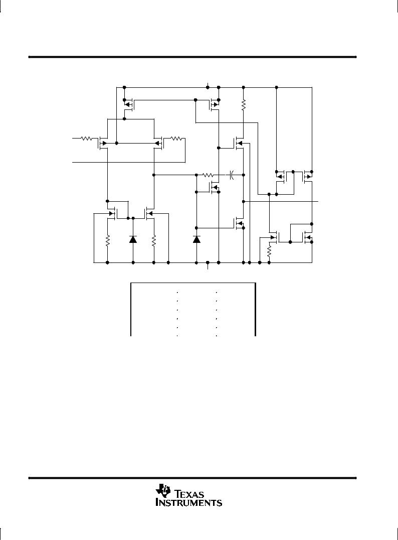
equivalent schematic (each amplifier)
|
|
|
VDD |
|
|
|
|
|
P3 |
P4 |
|
|
|
|
|
|
|
|
R6 |
|
P1 |
|
P2 |
|
N5 |
|
|
IN ± |
|
|
|
|
|
|
R1 |
|
|
R2 |
|
|
|
IN + |
|
|
|
C1 |
P5 |
P6 |
|
|
|
R5 |
|||
|
|
|
N3 |
|
|
OUT |
|
|
|
|
|
|
|
|
|
|
|
N4 |
|
|
|
N1 |
N2 |
|
|
N6 |
|
|
|
|
|
|
|
|
R3 |
D1 |
R4 |
D2 |
|
|
N7 |
|
|
|
||||
|
|
|
|
|
R7 |
|
|
|
|
GND |
|
|
|
ACTUAL DEVICE COMPONENT COUNT²
COMPONENT |
TLV2342 |
TLV2344 |
|
|
|
Transistors |
54 |
108 |
|
|
|
Resistors |
14 |
28 |
|
|
|
Diodes |
4 |
8 |
|
|
|
Capacitors |
2 |
4 |
²Includes both amplifiers and all ESD, bias, and trim circuitry.
4 |
POST OFFICE BOX 655303 •DALLAS, TEXAS 75265 |

TLV2322, TLV2322Y, TLV2324, TLV2324Y
LinCMOS LOW-VOLTAGE LOW-POWER
OPERATIONAL AMPLIFIERS
SLOS187 ± FEBRUARY 1997
absolute maximum ratings over operating free-air temperature (unless otherwise noted)²
Supply voltage, VDD (see Note 1) . . . . . . . . . . . . . . . . . . . . . . . . . . . . . . . . . . . . . . . |
. . . . . . . . . . . . . . . . . . . . . . 8 V |
Differential input voltage, VID (see Note 2) . . . . . . . . . . . . . . . . . . . . . . . . . . . . . . . |
. . . . . . . . . . . . . . . . . . . . VDD ± |
Input voltage range, VI (any input) . . . . . . . . . . . . . . . . . . . . . . . . . . . . . . . . . . . . . . . |
. . . . . . . . . . . . ±0.3 V to VDD |
Input current, II . . . . . . . . . . . . . . . . . . . . . . . . . . . . . . . . . . . . . . . . . . . . . . . . . . . . . . . |
. . . . . . . . . . . . . . . . . . . ± 5 mA |
Output current, IO . . . . . . . . . . . . . . . . . . . . . . . . . . . . . . . . . . . . . . . . . . . . . . . . . . . . . |
. . . . . . . . . . . . . . . . . . ± 30 mA |
Duration of short-circuit current at (or below) TA = 25°C (see Note 3) . . . . . . . . |
. . . . . . . . . . . . . . . . . unlimited |
Continuous total dissipation . . . . . . . . . . . . . . . . . . . . . . . . . . . . . . . . . . . . . . . . . . . |
See Dissipation Rating Table |
Operating free-air temperature range, TA . . . . . . . . . . . . . . . . . . . . . . . . . . . . . . . . |
. . . . . . . . . . . . ±40°C to 85°C |
Storage temperature range . . . . . . . . . . . . . . . . . . . . . . . . . . . . . . . . . . . . . . . . . . . . . |
. . . . . . . . . . . ±65°C to 150°C |
Lead temperature 1,6 mm (1/16 inch) from case for 10 seconds . . . . . . . . . . . . |
. . . . . . . . . . . . . . . . . . . 260°C |
²Stresses beyond those listed under ªabsolute maximum ratingsº may cause permanent damage to the device. These are stress ratings only, and functional operation of the device at these or any other conditions beyond those indicated under ªrecommended operating conditionsº is not implied. Exposure to absolute-maximum rated conditions for extended periods may affect device reliability.
NOTES: 1. All voltage values, except differential voltages, are with respect to network ground.
2.Differential voltages are at the noninverting input with respect to the inverting input.
3.The output may be shorted to either supply. Temperature and /or supply voltages must be limited to ensure that the maximum dissipation rating is not exceeded (see application section).
|
DISSIPATION RATING TABLE |
|
||
PACKAGE |
TA ≤ 25°C |
DERATING FACTOR |
TA = 85°C |
|
POWER RATING |
ABOVE TA = 25°C |
POWER RATING |
||
|
||||
D±8 |
725 mW |
5.8 mW/°C |
377 mW |
|
D±14 |
950 mW |
7.6 mW/°C |
494 mW |
|
N |
1575 mW |
12.6 mW/°C |
819 mW |
|
P |
1000 mW |
8.0 mW/°C |
520 mW |
|
PW±8 |
525 mW |
4.2 mW/°C |
273 mW |
|
PW±14 |
700 mW |
5.6 mW/°C |
364 mW |
|
|
|
|
|
|
recommended operating conditions
|
|
MIN |
MAX |
UNIT |
|
|
|
|
|
|
|
Supply voltage, VDD |
|
2 |
8 |
V |
|
Common-mode input voltage, VIC |
VDD = 3 V |
± 0.2 |
1.8 |
V |
|
VDD = 5 V |
± 0.2 |
3.8 |
|||
|
|
||||
Operating free-air temperature, TA |
|
± 40 |
85 |
°C |
POST OFFICE BOX 655303 •DALLAS, TEXAS 75265 |
5 |
TLV2322, TLV2322Y, TLV2324, TLV2324Y
LinCMOS LOW-VOLTAGE LOW-POWER
OPERATIONAL AMPLIFIERS
SLOS187 ± FEBRUARY 1997
TLV2322 electrical characteristics at specified free-air temperature
|
|
|
|
|
|
|
|
|
TLV2322 |
|
|
|
|
|
|
PARAMETER |
TEST CONDITIONS |
T ² |
|
|
|
|
|
|
|
|
UNIT |
||
|
V |
DD |
= 3 V |
|
V |
DD |
= 5 V |
|
||||||
|
|
|
|
|
A |
|
|
|
|
|
|
|
||
|
|
|
|
|
|
MIN |
TYP |
MAX |
MIN |
TYP |
MAX |
|
||
|
|
|
|
|
|
|
|
|
|
|
|
|
||
|
|
VO = 1 V, |
25°C |
|
|
1.1 |
9 |
|
|
1.1 |
9 |
|
||
VIO |
Input offset voltage |
VIC = 1 V, |
|
|
|
|
|
|
|
|
|
mV |
||
RS |
= 50 Ω, |
Full range |
|
|
|
11 |
|
|
|
11 |
||||
|
|
|
|
|
|
|
|
|
||||||
|
|
RL = 1 MΩ |
|
|
|
|
|
|
|
|||||
|
|
|
|
|
|
|
|
|
|
|
|
|||
αVIO |
Average temperature coefficient |
|
|
|
25°C to |
|
|
1 |
|
|
|
1.1 |
|
μV/°C |
of input offset voltage |
|
|
|
° |
|
|
|
|
|
|
||||
|
|
|
|
85 C |
|
|
|
|
|
|
|
|
|
|
IIO |
Input offset current (see Note 4) |
VO = 1 V, |
25°C |
|
|
0.1 |
|
|
|
0.1 |
|
pA |
||
|
|
|
|
|
|
|
|
|
||||||
V |
IC |
= 1 V |
° |
|
|
22 |
1000 |
|
|
24 |
1000 |
|||
|
|
|
|
85 C |
|
|
|
|
|
|||||
IIB |
Input bias current (see Note 4) |
VO = 1 V, |
25°C |
|
|
0.6 |
|
|
|
0.6 |
|
pA |
||
|
|
|
|
|
|
|
|
|
||||||
V |
IC |
= 1 V |
° |
|
|
175 |
2000 |
|
|
200 |
2000 |
|||
|
|
|
|
85 C |
|
|
|
|
|
|||||
|
|
|
|
|
|
± 0.2 |
± 0.3 |
|
± 0.2 |
± 0.3 |
|
|
||
|
|
|
|
|
25°C |
to |
|
to |
|
to |
|
to |
|
V |
VICR |
Common-mode input voltage |
|
|
|
|
2 |
|
2.3 |
|
4 |
|
4.2 |
|
|
|
|
|
|
|
|
|
|
|
|
|
|
|
||
range (see Note 5) |
|
|
|
|
± 0.2 |
|
|
|
± 0.2 |
|
|
|
|
|
|
|
|
|
|
|
|
|
|
|
|
|
|||
|
|
|
|
|
Full range |
to |
|
|
|
to |
|
|
|
V |
|
|
|
|
|
|
1.8 |
|
|
|
3.8 |
|
|
|
|
|
|
|
|
|
|
|
|
|
|
|
|
|
|
|
|
|
V |
IC |
= 1 V, |
° |
1.75 |
|
1.9 |
|
3.2 |
|
3.8 |
|
|
|
|
|
|
25 C |
|
|
|
|
|
|||||
VOH |
High-level output voltage |
VID = 100 mV, |
|
|
|
|
|
|
|
|
|
V |
||
Full range |
1.7 |
|
|
|
3 |
|
|
|
||||||
|
|
IOH = ± 1 mA |
|
|
|
|
|
|
|
|||||
|
|
V |
IC |
= 1 V, |
° |
|
|
115 |
150 |
|
|
95 |
150 |
|
|
|
|
|
25 C |
|
|
|
|
|
|||||
VOL |
Low-level output voltage |
VID = ± 100 mV, |
|
|
|
|
|
|
|
|
|
mV |
||
Full range |
|
|
|
190 |
|
|
|
190 |
||||||
|
|
IOL = 1 mA |
|
|
|
|
|
|
|
|||||
|
|
V |
IC |
= 1 V, |
° |
50 |
|
400 |
|
50 |
|
520 |
|
|
|
Large-signal differential voltage |
|
|
25 C |
|
|
|
|
|
|||||
AVD |
RL = 1 MΩ, |
|
|
|
|
|
|
|
|
|
V/mV |
|||
amplification |
Full range |
50 |
|
|
|
50 |
|
|
|
|||||
|
See Note 6 |
|
|
|
|
|
|
|
||||||
|
|
|
|
|
|
|
|
|
||||||
|
|
|
|
|
|
|
|
|
|
|
|
|
|
|
|
|
V |
O |
= 1 V, |
° |
65 |
|
88 |
|
65 |
|
94 |
|
|
|
|
|
|
25 C |
|
|
|
|
|
|||||
CMRR |
Common-mode rejection ratio |
VIC = VICR min, |
|
|
|
|
|
|
|
|
|
dB |
||
Full range |
60 |
|
|
|
60 |
|
|
|
||||||
|
|
RS = 50 Ω |
|
|
|
|
|
|
|
|||||
|
|
V |
IC |
= 1 V, |
° |
70 |
|
86 |
|
70 |
|
86 |
|
|
|
Supply-voltage rejection ratio |
|
|
25 C |
|
|
|
|
|
|||||
kSVR |
VO |
= 1 V, |
|
|
|
|
|
|
|
|
|
dB |
||
( VDD / VIO) |
Full range |
65 |
|
|
|
65 |
|
|
|
|||||
|
RS |
= 50 Ω |
|
|
|
|
|
|
|
|||||
|
|
|
|
|
|
|
|
|
||||||
IDD |
Supply current |
VO = 1 V, VIC = 1 V, |
25°C |
|
|
12 |
34 |
|
|
20 |
34 |
μA |
||
|
|
|
|
|
|
|
|
|
||||||
No load |
Full range |
|
|
|
54 |
|
|
|
54 |
|||||
|
|
|
|
|
|
|
|
|
||||||
² Full range is ± 40°C to 85°C.
NOTES: 4. The typical values of input bias current and input offset current below 5 pA are determined mathematically.
5.This range also applies to each input individually.
6.At VDD = 5 V, VO(PP) = 0.25 V to 2 V; at VDD = 3 V, VO = 0.5 V to 1.5
6 |
POST OFFICE BOX 655303 •DALLAS, TEXAS 75265 |
|
|
|
|
|
|
TLV2322, TLV2322Y, TLV2324, TLV2324Y |
||||||||||
|
|
|
|
|
LinCMOS |
LOW-VOLTAGE LOW-POWER |
||||||||||
|
|
|
|
|
|
|
|
OPERATIONAL AMPLIFIERS |
||||||||
|
|
|
|
|
|
|
|
|
|
SLOS187 ± FEBRUARY 1997 |
||||||
|
|
|
|
|
|
|
|
|
|
|
||||||
TLV2322 operating characteristics at specified free-air temperature, VDD = 3 V |
|
|
|
|
|
|
||||||||||
|
PARAMETER |
|
|
TEST CONDITIONS |
|
TA |
|
TLV2322 |
|
UNIT |
|
|
||||
|
|
|
|
|
|
|
|
|||||||||
|
|
|
|
MIN |
TYP |
MAX |
|
|
||||||||
|
|
|
|
|
|
|
|
|
|
|
|
|
||||
|
|
|
|
|
|
|
|
|
|
|
|
|
|
|
|
|
|
|
V |
|
= 1 V, |
V |
= 1 V, |
|
° |
|
0.02 |
|
|
|
|
|
|
|
|
IC |
I(PP) |
|
|
25 C |
|
|
|
|
|
|
|
|||
SR |
Slew rate at unity gain |
RL = 1 MΩ, |
CL = 20 pF, |
|
|
|
|
|
V/μs |
|
||||||
|
85°C |
|
0.02 |
|
|
|
||||||||||
|
|
See Figure 35 |
|
|
|
|
|
|
|
|
|
|
||||
|
|
|
|
|
|
|
|
|
|
|
|
|
|
|||
|
|
f = 1 kHz, |
RS = 20 Ω, |
|
25°C |
|
|
|
|
|
|
|
|
|||
Vn |
Equivalent input noise voltage |
|
|
68 |
|
nV/√ Hz |
|
|
||||||||
See Figure 36 |
|
|
|
|
|
|
||||||||||
|
|
|
|
|
|
|
|
|
|
|
|
|
|
|||
|
|
|
|
|
|
|
|
|
|
|
|
|
|
|
|
|
BOM |
Maximum output-swing bandwidth |
VO = VOH, |
CL = 20 pF, |
|
25°C |
|
2.5 |
|
kHz |
|
|
|||||
|
|
|
|
|
|
|
||||||||||
R |
L |
= 1 MΩ, |
See Figure 35 |
|
° |
|
2 |
|
|
|
||||||
|
|
|
|
|
|
|
85 C |
|
|
|
|
|
|
|
||
B1 |
Unity-gain bandwidth |
VI = 10 mV, |
CL = 20 pF, |
|
25°C |
|
27 |
|
kHz |
|
|
|||||
|
|
|
|
|
|
|
||||||||||
R |
L |
= 1 MΩ, |
See Figure 37 |
|
° |
|
21 |
|
|
|
||||||
|
|
|
|
|
|
|
85 C |
|
|
|
|
|
|
|
||
|
|
VI = 10 mV, |
f= B1, |
|
± 40°C |
|
39° |
|
|
|
|
|
|
|||
|
|
|
|
|
|
|
|
|
|
|
|
|
||||
φm |
Phase margin |
CL = 20 pF, |
RL = 1 MΩ, |
|
25°C |
|
34° |
|
|
|
|
|
|
|||
|
|
See Figure 37 |
|
|
|
85°C |
|
28° |
|
|
|
|
|
|
||
|
|
|
|
|
|
|
|
|
|
|
|
|
|
|
||
|
|
|
|
|
|
|
|
|
|
|
||||||
TLV2322 operating characteristics at specified free-air temperature, VDD = 5 V |
|
|
|
|
|
|
||||||||||
|
|
|
|
|
|
|
|
|
|
|
|
|
|
|
|
|
|
PARAMETER |
|
|
TEST CONDITIONS |
|
TA |
|
TLV2322 |
|
UNIT |
|
|
||||
|
|
|
|
|
|
|
|
|||||||||
|
|
|
|
MIN |
TYP |
MAX |
|
|
||||||||
|
|
|
|
|
|
|
|
|
|
|
||||||
|
|
|
|
|
|
|
|
|
|
|
|
|
|
|
|
|
|
|
VIC = 1 V, |
V |
= 1 V |
|
25°C |
|
0.03 |
|
|
|
|
|
|
||
|
|
|
|
|
|
|
|
|
|
|
|
|||||
|
|
|
85°C |
|
0.03 |
|
|
|
|
|
|
|||||
|
|
|
|
Ω |
I(PP) |
|
|
|
|
|
|
|
|
|
||
SR |
Slew rate at unity gain |
RL = 1 M , |
|
|
|
|
|
|
|
V/μs |
|
|
||||
C |
L |
= 20 pF, |
|
|
|
° |
|
0.03 |
|
|
|
|||||
|
|
|
|
|
|
|
|
|
|
|
|
|||||
|
|
|
|
VI(PP) = 2.5 V |
|
25 C |
|
|
|
|
|
|
|
|||
|
|
See Figure 35 |
|
|
|
|
|
|
|
|
|
|
||||
|
|
|
85°C |
|
0.02 |
|
|
|
|
|
|
|||||
|
|
|
|
|
|
|
|
|
|
|
|
|
|
|
||
|
|
|
|
|
|
|
|
|
|
|
|
|
|
|||
|
|
f = 1 kHz, |
RS = 20 Ω, |
|
25°C |
|
|
|
|
|
|
|
|
|||
Vn |
Equivalent input noise voltage |
|
|
68 |
|
nV/√ Hz |
|
|
||||||||
See Figure 36 |
|
|
|
|
|
|
||||||||||
|
|
|
|
|
|
|
|
|
|
|
|
|
|
|||
|
|
|
|
|
|
|
|
|
|
|
|
|
|
|
|
|
BOM |
Maximum output-swing bandwidth |
VO = VOH, |
CL = 20 pF, |
|
25°C |
|
5 |
|
kHz |
|
|
|||||
|
|
|
|
|
|
|
||||||||||
R |
L |
= 1 MΩ, |
See Figure 35 |
|
° |
|
4 |
|
|
|
||||||
|
|
|
|
|
|
|
85 C |
|
|
|
|
|
|
|
||
B1 |
Unity-gain bandwidth |
VI = 10 mV, |
CL = 20 pF, |
|
25°C |
|
85 |
|
kHz |
|
|
|||||
|
|
|
|
|
|
|
||||||||||
R |
L |
= 1 MΩ, |
See Figure 37 |
|
° |
|
55 |
|
|
|
||||||
|
|
|
|
|
|
|
85 C |
|
|
|
|
|
|
|
||
|
|
VI = 10 mV, |
f = B1, |
|
± 40°C |
|
38° |
|
|
|
|
|
|
|||
|
|
|
|
|
|
|
|
|
|
|
|
|
||||
φm |
Phase margin |
CL = 20 pF, |
RL = 1 MΩ, |
|
25°C |
|
34° |
|
|
|
|
|
|
|||
|
|
See Figure 37 |
|
|
|
85°C |
|
28° |
|
|
|
|
|
|
||
|
|
|
|
|
|
|
|
|
|
|
|
|
|
|
||
|
|
|
|
|
|
|
|
|
|
|
|
|
|
|
|
|
POST OFFICE BOX 655303 •DALLAS, TEXAS 75265 |
7 |

TLV2322, TLV2322Y, TLV2324, TLV2324Y
LinCMOS LOW-VOLTAGE LOW-POWER
OPERATIONAL AMPLIFIERS
SLOS187 ± FEBRUARY 1997
TLV2324I electrical characteristics at specified free-air temperature
|
|
|
|
|
|
|
|
|
TLV2324I |
|
|
|
|
|
|
PARAMETER |
TEST CONDITIONS |
T ² |
|
|
|
|
|
|
|
|
UNIT |
||
|
V |
DD |
= 3 V |
|
V |
DD |
= 5 V |
|
||||||
|
|
|
|
|
A |
|
|
|
|
|
|
|
||
|
|
|
|
|
|
MIN |
TYP |
MAX |
MIN |
TYP |
MAX |
|
||
|
|
|
|
|
|
|
|
|
|
|
|
|
||
|
|
VO = 1 V, |
25°C |
|
|
1.1 |
10 |
|
|
1.1 |
10 |
|
||
VIO |
Input offset voltage |
VIC = 1 V, |
|
|
|
|
|
|
|
|
|
mV |
||
RS = 50 Ω, |
Full range |
|
|
|
12 |
|
|
|
12 |
|||||
|
|
|
|
|
|
|
|
|
||||||
|
|
RL = 1 MΩ, |
|
|
|
|
|
|
|
|||||
|
|
|
|
|
|
|
|
|
|
|
|
|||
αVIO |
Average temperature coefficient |
|
|
|
25°C to |
|
|
1 |
|
|
|
1.1 |
|
μV/°C |
of input offset voltage |
|
|
|
85°C |
|
|
|
|
|
|
||||
|
|
|
|
|
|
|
|
|
|
|
|
|
||
|
|
|
|
|
|
|
|
|
|
|
|
|
|
|
IIO |
Input offset current (see Note 4) |
VO = 1 V, |
25°C |
|
|
0.1 |
|
|
|
0.1 |
|
pA |
||
|
|
|
|
|
|
|
|
|
||||||
V |
IC |
= 1 V |
° |
|
|
22 |
1000 |
|
|
24 |
1000 |
|||
|
|
|
|
85 C |
|
|
|
|
|
|||||
IIB |
Input bias current (see Note 4) |
VO = 1 V, |
25°C |
|
|
0.6 |
|
|
|
0.6 |
|
pA |
||
|
|
|
|
|
|
|
|
|
||||||
V |
IC |
= 1 V |
° |
|
|
175 |
2000 |
|
|
200 |
2000 |
|||
|
|
|
|
85 C |
|
|
|
|
|
|||||
|
|
|
|
|
|
± 0.2 |
± 0.3 |
|
± 0.2 |
± 0.3 |
|
|
||
|
|
|
|
|
25°C |
to |
|
to |
|
to |
|
to |
|
V |
VICR |
Common-mode input |
|
|
|
|
2 |
|
2.3 |
|
4 |
|
4.2 |
|
|
|
|
|
|
|
|
|
|
|
|
|
|
|
||
voltage range (see Note 5) |
|
|
|
|
± 0.2 |
|
|
|
± 0.2 |
|
|
|
|
|
|
|
|
|
|
|
|
|
|
|
|
|
|||
|
|
|
|
|
Full range |
to |
|
|
|
to |
|
|
|
V |
|
|
|
|
|
|
1.8 |
|
|
|
3.8 |
|
|
|
|
|
|
|
|
|
|
|
|
|
|
|
|
|
|
|
|
|
V |
IC |
= 1 V, |
° |
1.75 |
|
1.9 |
|
3.2 |
|
3.8 |
|
|
|
|
|
|
25 C |
|
|
|
|
|
|||||
VOH |
High-level output voltage |
VID = 100 mV, |
|
|
|
|
|
|
|
|
|
V |
||
Full range |
1.7 |
|
|
|
3 |
|
|
|
||||||
|
|
IOH = ± 1 mA |
|
|
|
|
|
|
|
|||||
|
|
V |
IC |
= 1 V, |
° |
|
|
115 |
150 |
|
|
95 |
150 |
|
|
|
|
|
25 C |
|
|
|
|
|
|||||
VOL |
Low-level output voltage |
VID = ±100 mV, |
|
|
|
|
|
|
|
|
|
mV |
||
Full range |
|
|
|
190 |
|
|
|
190 |
||||||
|
|
IOL = 1 mA |
|
|
|
|
|
|
|
|||||
|
|
V |
IC |
= 1 V, |
° |
50 |
|
400 |
|
50 |
|
520 |
|
|
|
Large-signal differential |
|
|
25 C |
|
|
|
|
|
|||||
AVD |
RL = 1 MΩ, |
|
|
|
|
|
|
|
|
|
V/mV |
|||
voltage amplification |
Full range |
50 |
|
|
|
50 |
|
|
|
|||||
|
See Note 6 |
|
|
|
|
|
|
|
||||||
|
|
|
|
|
|
|
|
|
||||||
|
|
|
|
|
|
|
|
|
|
|
|
|
|
|
|
|
V |
O |
= 1 V, |
° |
65 |
|
88 |
|
65 |
|
94 |
|
|
|
|
|
|
25 C |
|
|
|
|
|
|||||
CMRR |
Common-mode rejection ratio |
VIC = VICRmin, |
|
|
|
|
|
|
|
|
|
dB |
||
Full range |
60 |
|
|
|
60 |
|
|
|
||||||
|
|
RS = 50 Ω |
|
|
|
|
|
|
|
|||||
kSVR |
Supply-voltage rejection ratio |
VIC = 1 V, VO = 1 V, |
25°C |
70 |
|
86 |
|
70 |
|
86 |
|
dB |
||
|
|
|
|
|
|
|
|
|
||||||
( VDD / VIO) |
RS = 50 Ω |
Full range |
65 |
|
|
|
65 |
|
|
|
||||
|
|
|
|
|
|
|
|
|||||||
|
|
VO = 1 V, VIC = 1 V, |
25°C |
|
|
24 |
68 |
|
|
39 |
68 |
μ |
||
IDD |
Supply current |
No load |
|
|
|
|
|
|
|
|
|
A |
||
Full range |
|
|
|
108 |
|
|
|
108 |
||||||
|
|
|
|
|
|
|
|
|
||||||
|
|
|
|
|
|
|
|
|
|
|
|
|||
|
|
|
|
|
|
|
|
|
|
|
|
|
|
|
² Full range is ± 40°C to 85°C. |
|
|
|
|
|
|
|
|
|
|
|
|
|
|
NOTES: |
4. The typical values of input bias current and input offset current below 5 pA are determined mathematically. |
|
|
|||||||||||
5.This range also applies to each input individually.
6.At VDD = 5 V, VO(PP) = 0.25 V to 2 V; at VDD = 3 V, VO = 0.5 V to 1.5 V.
8 |
POST OFFICE BOX 655303 •DALLAS, TEXAS 75265 |

|
|
|
|
|
TLV2322, TLV2322Y, TLV2324, TLV2324Y |
||||||||||
|
|
|
|
|
LinCMOS |
LOW-VOLTAGE LOW-POWER |
|||||||||
|
|
|
|
|
|
|
OPERATIONAL AMPLIFIERS |
||||||||
|
|
|
|
|
|
|
|
|
SLOS187 ± FEBRUARY 1997 |
||||||
|
|
|
|
|
|
|
|
|
|
|
|||||
TLV2324I operating characteristics at specified free-air temperature, VDD = 3 V |
|
|
|
|
|
|
|||||||||
|
PARAMETER |
|
|
TEST CONDITIONS |
|
TA |
|
TLV2324I |
|
UNIT |
|
||||
|
|
|
|
|
|
|
|
||||||||
|
|
|
|
MIN |
TYP |
MAX |
|
||||||||
|
|
|
|
|
|
|
|
|
|
|
|
|
|||
|
|
|
|
|
|
|
|
|
|
|
|
|
|
||
|
|
VIC = 1 V, |
VI(PP) = 1 V, |
|
25°C |
|
0.02 |
|
|
|
|
|
|
||
SR |
Slew rate at unity gain |
RL = 1 MΩ, |
CL = 20 pF, |
|
|
|
|
|
V/μs |
|
|||||
|
85°C |
|
0.02 |
|
|
||||||||||
|
|
See Figure 35 |
|
|
|
|
|
|
|
|
|
||||
|
|
|
|
|
|
|
|
|
|
|
|
|
|
||
Vn |
Equivalent input noise voltage |
f = 1 kHz, |
RS = 20 Ω, |
|
25°C |
|
68 |
|
|
|
|
|
|
||
|
|
|
nV√ /Hz |
|
|||||||||||
See Figure 36 |
|
|
|
|
|
||||||||||
|
|
|
|
|
|
|
|
|
|
|
|
|
|||
|
|
|
|
|
|
|
|
|
|
|
|
|
|
|
|
BOM |
Maximum output-swing bandwidth |
VO = VOH, |
CL = 20 pF, |
|
25°C |
|
2.5 |
|
kHz |
|
|||||
|
|
|
|
|
|
||||||||||
R |
L |
= 1 MΩ, |
See Figure 35 |
|
° |
|
2 |
|
|
||||||
|
|
|
|
|
|
85 C |
|
|
|
|
|
|
|
||
B1 |
Unity-gain bandwidth |
VI = 10 mV, |
CL = 20 pF, |
|
25°C |
|
27 |
|
kHz |
|
|||||
|
|
|
|
|
|
||||||||||
R |
L |
= 1 MΩ, |
See Figure 37 |
|
° |
|
21 |
|
|
||||||
|
|
|
|
|
|
85 C |
|
|
|
|
|
|
|
||
|
|
VI = 10 mV, |
f = B1, |
|
± 40°C |
|
39° |
|
|
|
|
|
|
||
|
|
|
|
|
|
|
|
|
|
|
|
||||
φm |
Phase margin |
CL = 20 pF, |
RL = 1 MΩ, |
|
25°C |
|
34° |
|
|
|
|
|
|
||
|
|
See Figure 37 |
|
|
85°C |
|
28° |
|
|
|
|
|
|
||
|
|
|
|
|
|
|
|
|
|
|
|
|
|
||
|
|
|
|
|
|
|
|
|
|
|
|||||
TLV2324I operating characteristics at specified free-air temperature, VDD = 5 V |
|
|
|
|
|
|
|||||||||
|
|
|
|
|
|
|
|
|
|
|
|
|
|
|
|
|
PARAMETER |
|
|
TEST CONDITIONS |
|
TA |
|
TLV2324I |
|
UNIT |
|
||||
|
|
|
|
|
|
|
|
||||||||
|
|
|
|
MIN |
TYP |
MAX |
|
||||||||
|
|
|
|
|
|
|
|
|
|
|
|||||
|
|
|
|
|
|
|
|
|
|
|
|
|
|
|
|
|
|
VIC = 1 V, |
V = 1 V |
|
25°C |
|
0.03 |
|
|
|
|
|
|
||
|
|
|
|
|
|
|
|
|
|
|
|
||||
|
|
|
85°C |
|
0.03 |
|
|
|
|
|
|
||||
|
|
|
|
Ω |
I(PP) |
|
|
|
|
|
|
|
|
||
SR |
Slew rate at unity gain |
RL = 1 M , |
|
|
|
|
|
|
V/μs |
|
|||||
C |
L |
= 20 pF, |
|
|
° |
|
0.03 |
|
|
||||||
|
|
|
|
|
|
|
|
|
|
|
|||||
|
|
|
|
VI(PP) = 2.5 V |
|
25 C |
|
|
|
|
|
|
|
||
|
|
See Figure 35 |
|
|
|
|
|
|
|
|
|
|
|||
|
|
|
85°C |
|
0.02 |
|
|
|
|
|
|
||||
|
|
|
|
|
|
|
|
|
|
|
|
|
|
||
|
|
|
|
|
|
|
|
|
|
|
|
|
|
||
Vn |
Equivalent input noise voltage |
f = 1 kHz, |
RS = 20 Ω, |
|
25°C |
|
68 |
|
|
|
|
|
|
||
|
|
|
nV/√ Hz |
|
|||||||||||
See Figure 36 |
|
|
|
|
|
||||||||||
|
|
|
|
|
|
|
|
|
|
|
|
|
|||
|
|
|
|
|
|
|
|
|
|
|
|
|
|
|
|
BOM |
Maximum output-swing bandwidth |
VO = VOH, |
CL = 20 pF, |
|
25°C |
|
5 |
|
kHz |
|
|||||
|
|
|
|
|
|
||||||||||
R |
L |
= 1 MΩ, |
See Figure 35 |
|
° |
|
4 |
|
|
||||||
|
|
|
|
|
|
85 C |
|
|
|
|
|
|
|
||
B1 |
Unity-gain bandwidth |
VI = 10 mV, |
CL = 20 pF, |
|
25°C |
|
85 |
|
kHz |
|
|||||
|
|
|
|
|
|
||||||||||
R |
L |
= 1 MΩ, |
See Figure 37 |
|
° |
|
55 |
|
|
||||||
|
|
|
|
|
|
85 C |
|
|
|
|
|
|
|
||
|
|
VI = 10 mV, |
f = B1, |
|
± 40°C |
|
38° |
|
|
|
|
|
|
||
|
|
|
|
|
|
|
|
|
|
|
|
||||
φm |
Phase margin |
CL = 20 pF, |
RL = 1 MΩ, |
|
25°C |
|
34° |
|
|
|
|
|
|
||
|
|
See Figure 37 |
|
|
85°C |
|
28° |
|
|
|
|
|
|
||
|
|
|
|
|
|
|
|
|
|
|
|
|
|
||
|
|
|
|
|
|
|
|
|
|
|
|
|
|
|
|
POST OFFICE BOX 655303 •DALLAS, TEXAS 75265 |
9 |

TLV2322, TLV2322Y, TLV2324, TLV2324Y
LinCMOS LOW-VOLTAGE LOW-POWER
OPERATIONAL AMPLIFIERS
SLOS187 ± FEBRUARY 1997
TLV2322Y electrical characteristics, TA = 25°C
|
|
|
|
|
TLV2322Y |
|
|
|
|
|
|
|
|
|
|
|
|
|
PARAMETER |
TEST CONDITIONS |
VDD = 3 V |
|
VDD = 5 V |
|
UNIT |
|
|
|
|
|
MIN TYP |
MAX |
MIN TYP |
MAX |
|
|
|
|
|
|
|
|
|
|
VIO |
Input offset voltage |
VO = 1 V, |
VIC = 1 V, |
1.1 |
|
1.1 |
|
mV |
RS = 50 Ω, |
RL = 1 MΩ |
|
|
|||||
|
|
|
|
|
|
|
||
IIO |
Input offset current (see Note 4) |
VO = 1 V, |
VIC = 1 V |
0.1 |
|
0.1 |
|
pA |
IIB |
Input bias current (see Note 4) |
VO = 1 V, |
VIC = 1 V |
0.6 |
|
0.6 |
|
pA |
|
Common-mode input voltage |
|
|
± 0.3 |
|
± 0.3 |
|
|
VICR |
|
|
to |
|
to |
|
V |
|
range (see Note 5) |
|
|
|
|
||||
|
|
|
2.3 |
|
4.2 |
|
|
|
|
|
|
|
|
|
|
||
|
|
|
|
|
|
|
|
|
VOH |
High-level output voltage |
VIC = 1 V, |
VID = ± 100 mV, |
1.9 |
|
3.8 |
|
V |
IOH = ± 1 mA |
|
|
|
|||||
|
|
|
|
|
|
|
|
|
VOL |
Low-level output voltage |
VIC = 1 V, |
VID = 100 mV, |
115 |
|
95 |
|
mV |
IOL = 1 mA |
|
|
|
|||||
|
|
|
|
|
|
|
|
|
AVD |
Large-signal differential voltage |
VIC = 1 V, |
RL = 1 MΩ, |
400 |
|
520 |
|
V/mV |
amplification |
See Note 6 |
|
|
|
||||
|
|
|
|
|
|
|
||
|
|
|
|
|
|
|
|
|
CMRR |
Common-mode rejection ratio |
VO = 1 V, |
VIC = VICR min, |
88 |
|
94 |
|
dB |
RS = 50 Ω |
|
|
|
|||||
|
|
|
|
|
|
|
|
|
kSVR |
Supply-voltage rejection ratio |
VO = 1 V, |
VIC = 1 V, |
86 |
|
86 |
|
dB |
( VDD / VID) |
RS = 50 Ω |
|
|
|
||||
|
|
|
|
|
|
|
||
IDD |
Supply current |
VO = 1 V, |
VIC = 1 V, |
12 |
|
20 |
|
μA |
No load |
|
|
|
|||||
|
|
|
|
|
|
|
|
|
|
|
|
|
|
|
|||
NOTES: 4. The typical values of input bias current offset current below 5 pA are determined mathematically. |
|
|
||||||
5.This range also applies to each input individually.
6.At VDD = 5 V, VO = 0.25 V to 2 V; at VDD = 3 V, VO = 0.5 V to 1.5 V.
10 |
POST OFFICE BOX 655303 •DALLAS, TEXAS 75265 |
 Loading...